


 text new page (beta)
 English (pdf)
 Article in xml format
 Article references
 Send this article by e-mail
 Cited by SciELO
  Similars in
SciELO
Similars in
SciELO 
 Permalink
1. INTRODUCTION
Due to the requirement of alternative energy sources in near future, an intense investigation has been made towards the solar energy harvesting (Bishnoi & Chawla, 2017; Saravanan & Babu, 2017), where the solar energy is converted into electricity by means of electron-hole pair generation in a semiconductor device. In the solar industry, amorphous silicon (a-Si) is one of the promising photovoltaic (solar) materials used for solar cell fabrication due to its nontoxicity, abundance, mature processing technology. Additionally, the effective optical absorption depth of a-Si is only about 1 µm , ie., 2 orders of magnitude less than that of crystalline silicon, which favors to the fabrication of thin film solar cell.
The major factor that affeets the efficieney of a thin film solar cell are the low absorption of Si in the infrared región and the reflection loss from the front side of the device. The up-conversion of infrared región and followed by the absorption in Si layer improves the optical conversión efficieney (Bishnoi & Chawla, 2017). The front side reflection is arise due the optical impedance mismatch (due to the difference of refractive Índices, r.i.) of air and a-Si is primarily responsible for such behavior. One of the well-known technique to reduce the reflection loss is surface texturing, but this cost to high surface recombination center of the minority carriers (Voroshilov, Simovski, Belov, & Shalin, 2015; Wang et al., 2009).
Therefore, the alternative technique, like quarter wavelength anti-reflection coating (ARC) is the most favorable solution and widely used. Over the years several materials have been demonstrated as an ARC; like: TiO2 (r.i.= 2.3), Si3N4 (r.i. = 1.9), A12O3 (r.i.= 1.8-1.9), SiO2 (r.i.= 1.4-1.5), Ta2O5 (r.i.= 2.1-2.3) (Green, 1982; Jang, Song, Choi, Yu, & Lee, 2011). Among them, silicon nitride (SiNx) is the most common material used for silicon solar cell (Iwahashi et al., 2015). The ARC must be transparent in the visible región to reduce optical loss and must be highly conductive to serve as a front contact for the thin film solar cells. The SiNx is disadvantageous due to insulating nature. Therefore, in this work indium tin oxide (ITO, transparent and conducting) was considered as an ARC material, which can serve as a top electrode contact for the a-Si thin film solar cell as well. Furthermore, a back reflector was used to minimize the transmission loss of the solar cell.
Silicon is a poor absorber of light at the higher wavelength (greater than 700 nm) región of the solar spectrum. A thick semiconducting layer is required to trap that región of the solar spectrum, but this may reduce the efficieney of photogenerated carrier collection (the minority carrier diffusion length in the a-Si is ~300 nm (Jang, 2011)). Thinning of active material thickness may solve the problem, but at the cost of the effective light absorption in the active región. Efficient light trapping along with effective carrier collection is the key requirement to realize the efficient performance of a solar cell. The promising solution to trap the light effectively is the incorporation of nanostructure in the solar cell (Eisenlohr et al., 2014; Pattnaik, Chakravarty, Biswas, Dalal, & Slafer, 2014). The nanostructures scatter the light in the active materials and increase the path length in it. And it is well known that if the scattering angle inside the a-Si become more than 16°, the light will be trapped inside the active región (a-Si) (Atwater & Polman, 2010) and thus the performance of solar cell will improve. Therefore, metallic nanostructures were included in the active región of the solar cell to improve the performance.
In this work, we are presenting simulation results of optimization ITO thickness (dITO) as an efficient antireflection coating on a-Si. Further, the simulation was done with the nanostructured back reflector to study the enhancement of the light trapping in the solar cell. All simulations were performed using CST Microwave Studio.
2. DESIGN AND SIMULATION
2.1 ITO AS ANTIREFLECTION COATING
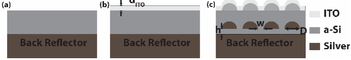
The proposed structure of an a-Si solar cell with the anti-reflection coating and a back reflector is shown in the Figure 1(a-c) (a 3D schematic is shown in Figure 9(b) ). To understand the effect of the ARC we have performed full wave simulation of bare a-Si/back metal and ITO/a-Si/back metal structures. The performance of the device with ITO-coated was compared with the standard 60 nm SiN-coated sample (simulated results of SiN/a-Si/back reflector). The thickness of the ITO was varied from 40 to 105 nm to optimize at the minimum average reflection (maximize the absorption in a-Si) from the structure in the spectral región of interest (350-800 nm). The thickness of the a-Si is considered to be 250 nm and silver (of thickness 250 nm) was used etS el back reflector and nanoparticle material. The optical properties of the a-Si, ITO, Al and SiN were taken from previously published literatures (Bååk, 1982; Optical Data from Sopra SA. (n.d); Palik, 1991).
2.2 PLASMONIC LIGHT TRAPPING IN THIN-FILM SOLAR CELL
It is well known that beyond 700 nm of the solar spectrum, the reflection loss of an a-Si solar cell is very high (Jang et al., 2011). Such characteristic is attributed to the low absorption coefficient of a-Si at that spectral región (Jang et al., 2011). Back side nano-structuring is one of the promising techniques to trap the light in the spectral región (700 - 800 nm) (Dijk et al., 2016; Mendes. Morawiec, Simone, Priolo, & Crupi, 2014; Pattnaik et al.. 2014). Generally, nanostructures scatter light homogeneously when it placed in a homogeneous médium, but the consequence changes when it placed near the interface of two media. The light will then scatter more in the higher dielectric médium compared to the lower dielectric medium(Atwater & Polman, 2010; Mertz, 2000). The scattered light takes an angular spread inside the dielectric médium and increases its path length. Henee, if the nanoparticles are placed in a-Si, the light inside the a-Si will scatter and the optical path length will be increased within it, thus the effective absorption will increase. This in-coupling of light in the semiconductor was first observed by Stuart and Hall (1996). And in 1998 they had implemented this idea for silicon photodetector (Stuart & Hall, 1998) and demonstrated a 20-fold increase in photocurrent.
In this work, to maximize the optical absorption at the near infrared región, half-spherical nanostructures (HSNS) were used. The diameters (D) and the positions (h) (from the bottom of the a-Si to the center of the particle) of the nanostructures were varied from 50-190 and 0-90 nm respectively (shown in: Figure 1(c)) and further the simulation was performed to determine the absorption and reflection of the device. Such structure can be fabricated by using the techniques described by Nam, Yoo, and Song (2016) . To compare the performances of different structures of solar cell, the average absorption (Ã) and the reflection ( R̃ ) in the optical spectrum were determined using the following relations in the spectral región 350-800 nm,
Where A(λ) and R(λ) are absolute absorption and absolute reflection at the corresponding wavelength (λ) respectively.
3. RESULT AND DISCUSSION
3.1 OPTIMIZATION OF ITO THICKNESS
A bare a-Si solar cell only with the back reflector was simulated to understand the effect of ARC. The reflection and absorption characteristic of a bare a-Si with a back reflector is shown in Figure 2. It can be observed that the reflection by the a-Si at the lower wavelength (<500 nm) región is high which is attributed to the impedance mismatch. Whereas in higher wavelength (>700 nm) región high reflection is observed which is appearing due to the low absorption coefficient of a-Si at that región.
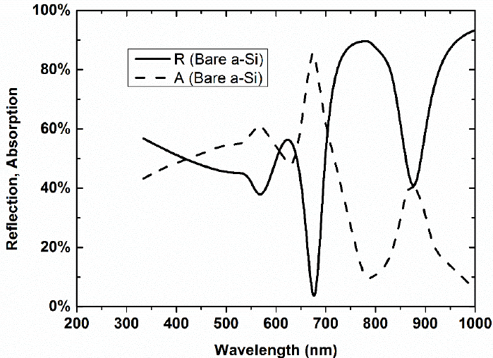
These high reflection losses will contribute to low absorption in the solar cell and will lead to low efficieney. However, an absorption peak at 875.6 nm is appearing due to the cavity resonance inside the a-Si región. The resonance is oceurring due to the interference of the reflected wave (from the back reflector) and the incident wave.
The à and R̃ for the bare silicon with a back reflector was calculated and found to be 47.5% and 52.5% respectively. This observation indicates that the structure has considerable amount of reflection loss that will certainly diminish the device performance. Therefore, to achieve a better performance, ITO as an ARC layer on the a-Si was used in this case. The thickness of the ITO plays a crucial role in the performance of solar cell since it works on the principie of quarter wavelength destructive interference. According to the principie, the reflected light and transmitted light interfere destructively and thus it acts like an anti-reflection coating. In order to obtain such condition, the thickness (d) of the anti-reflection coating must satisfy the relation,
Where, d and n (=(r.i. ambient x r.i. substrate)) are the thickness and refractive index (r.i.) of the ARC layer respectively. Considering the peak emission of solar spectrum at 500 nm (λ) and n is 1.7 to 2 (for ITO), the thickness should be ~60~65 nm. To optimize more aecurate valué of 'dITO' (thickness of ITO as ARC), the thickness was varied from 40 to 105 nm, and consequently à and 𝑹̃ were determined. The plot of optimization is illustrated in the Figure 3. From the figure, it can be verified that initially with the increase of the thickness of ITO, the reflection decreases and the absorption increases; but beyond - 65 nm, this behavior changes oppositely. The reflection spectrum does not changes significantly for the thickness 55-70 nm of ITO, therefore for this case a 65 nm thick ITO was considered as an optimized parameter.
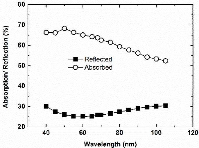
Fig. 3 Optimization of the drro to obtain máximum average absorption and mínimum average reflection. The considered spectrum is 400-800 nm.
The reflection and absorption spectrum of the 65 nm ITO/a-Si are shown in the Figure 4(a) and (b) respectively. In addition, the comparison with standard 60 nm SiN ARC coated on a-Si and bare Si is shown. It can be observed that in case of AR coated device the reflection ( R̃ ~25%) from the structure have reduced effectively and consequently absorption in a-Si (Ã~66%) increases. A slight amount (~9%) of loss is observed which is due to the transmission loss through the ITO.
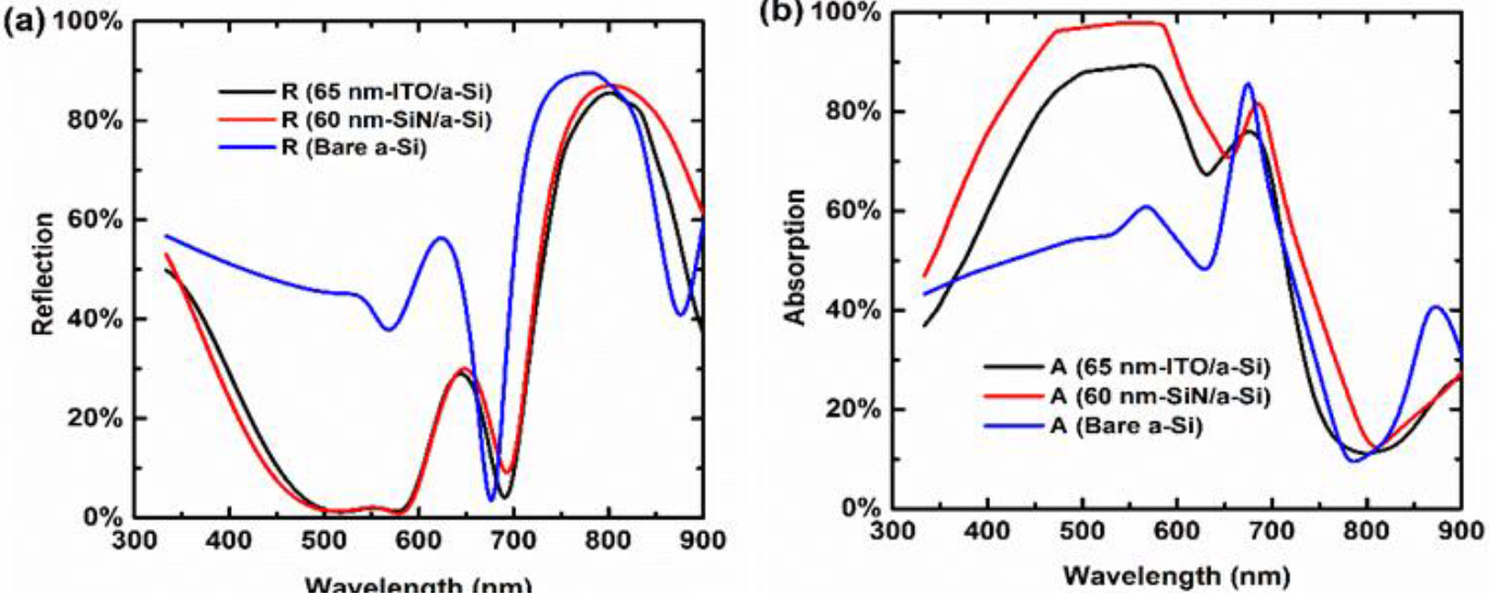
Fig. 4 Comparison of (a) reflection and (b) the absorption spectrum of the solar cell at different configuration.
Although use of 60 nm SiN (loss 4%) as an ARC can reduce the transmission loss but ITO has its advantage that is, it can be used as a top contact electrode due to its conductive property. Therefore, in this work ITO was used as an alternative ARC material.
3.2 NANOSTRUCTURING AND ENHANCEMENT IN PERFORMANCE
It can be observed from Figure 4, that beyond 700 nm the reflection from the solar cell increases sharply. This is due to the low absorption by a-Si and the reflection from back metal (since all the structure exhibit similar characteristics). The reflection can be minimized by diverting the incident light for the lateral propagation into the active médium. To achieve that Atwater and Polman, (2010), have used plasmonic nanostructures and have demonstrated significant improvement in performance in the solar cell.
The nanostructures inserted in semiconductor región scatter light inside the active médium and increases the path length. Additionally, they genérate surface plasmons and stimulate the lateral propagation (or guided propagation) of light inside the active médium. Thus, the effective path length increases and consequently the absorption of light enhances. In order to maximize the absorption of light in the active médium, the position (h) and the diameter (D) of the HSNS in the active médium were varied and consequent à were determined. The cross sectional schematic of the device is shown in the Figure 1 (c) (in this conformal growth of the thin film was assumed and a slight change in performance has been observed if a combination of conformal and isotropy growth condition will be considered, see supplementary data). During the optimization of D and h, the gap (w) between two nanoparticle was considered as 40 nm. The contour mapping of à against the parameters h, and D is shown in the Fig. 5. It can be observed from the figure that the valué of à is high at Rl and R2. This attribute to the generation of plasmonic wave at the interface of Si and metal. For the simplicity of fabrication process, in this case, región 'Rl' was considered as an optimized parameter for simulation.
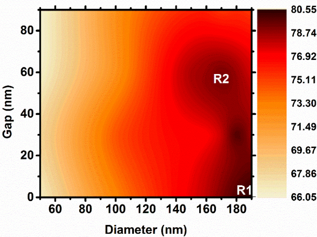
Fig. 5 Absorption plot by a-Si to optimize the position and diameter of the nano partidle in the solar cell.
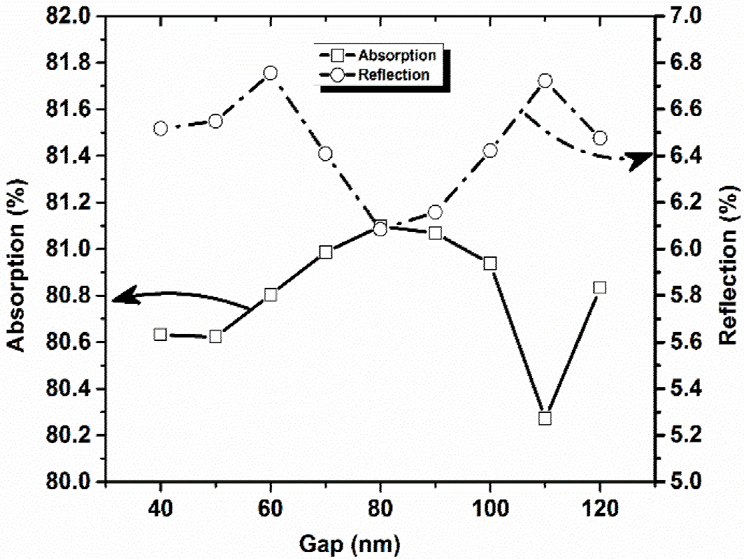
Further, to obtain the máximum absorption in a-Si, the gap (w) between two particles was varied from 40 to 120 nm. The variation ofi? and à with different 'w' were investigated and shown in the Figure 6. The figure indicates that the average absorption in a-Si (Ã) is almost constant over the range of w. However, at w=80 nm, the à (~81%) and 𝑹̃ (~6%) shows their máxima and minima respectively. Therefore, to compare the performance of the nano structure embedded device with the non-structured device, the valúes of D, w and h were considered to be 190 nm, 80 nm and 0 nm respectively.
The comparison of the reflectance and absorption spectrum of the devices with and without nanoparticle are shown in Figure 7. The figure clearly indicates that the device performance has improved significantly when the nanostructured (of size D=190 nm and w=80 nm at h=0) back reflector is incorporated. The enhancement in absorption can be explained by the generation of surface plasmon by the HSNS. From the Figure 8(c) and (d) , it is evident that the power flow directions (Poynting vectors) of the propagating wave (shown in the Figure 8(c) and (d) ) are tangential inside the a-Si.
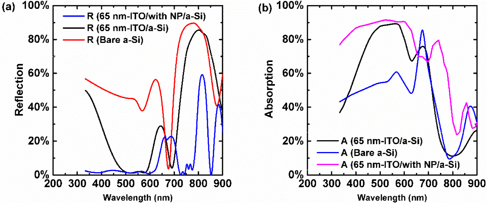
Fig. 7 Comparison of a) reflection spectrum and b) the absorption spectrum of the solar cell at different configuration of solar cell.
The incident wave propagation vector of the light is considered along the z-axis, which can be observed at the outside of the structure (in Figure 8(c) and (d) ). But, as the light enters in the structure, it starts to propágate laterally, this results to increase in the optical path in a-Si. Thus, the optical absorption by a-Si increases effectively. Although, a small degradation of absorption in the visible región (657-694 nm) is observed, but spectral absorption enhances significantly (-80%). The optical power loss in the structure is shown in the Figure 8(a) and (b) , which shows that most of the power is absorbed in the a-Si región. This characteristic is required to enhance the photocarrier generation and the quantum efficieney of the device.
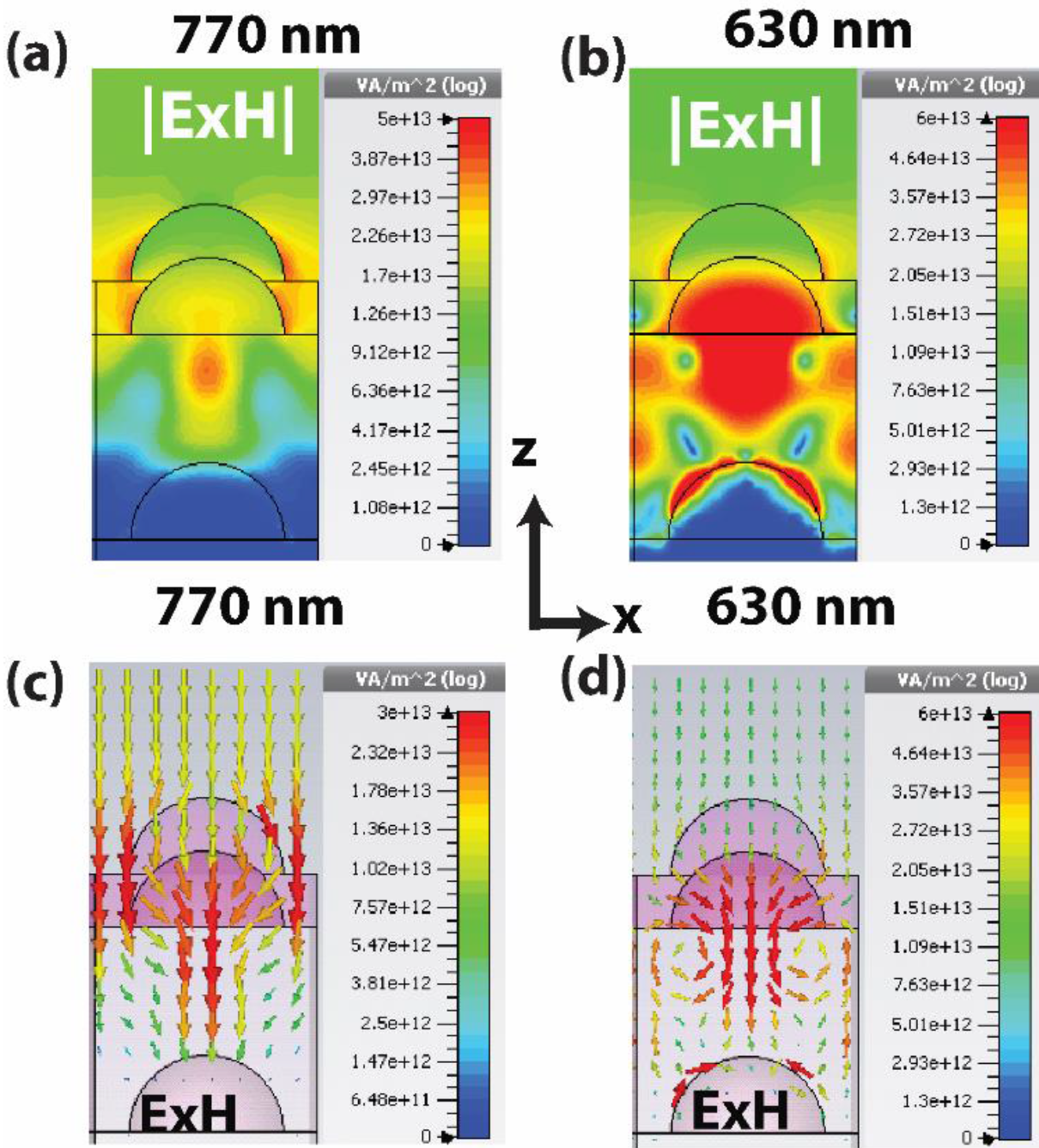
Fig. 8 Simulation results of the power loss in the structure at the (a) wavelength 630 nm and (b) 770 nm. The power flow or Poynting vector direction in the structure at the (c) wavelength 630 nm and (d) 770 nm.
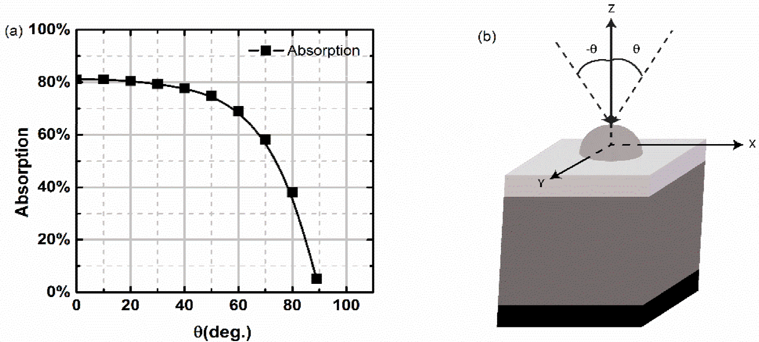
Finally, the performance the solar cell was investigated under the oblique incidence of light to study the angular coverage of the solar cell. The angle was varied with respect to normal of the solar plañe (with respected to the z-axis as shown in . The performance of the cell was calculated by irradiating a fixed amount of light to the cell. It can be observed from Figure 9(a) that the absorption of the solar cell is significant (varies 81% to 60%) for the incident angle of 0 to 70 deg and decrease sharply after that. This characteristic indicates that the proposed structure has large angular coverage. Henee, it can be concluded that the ITO ARC along with nanostructures at the backside can enhance the optical absorption in the a-Si thin film solar cell in the visible and near infrared región with large angular coverage.
4. CONCLUSION
In this paper, ITO was used as an alternative ARC for an a-Si thin film solar cell in order to achieve a broadband anti-reflection property in the visible and near infrared región (350 - 800 nm) of the spectrum. The thickness of the ITO was varied and the optimized valué was found to be 65 nm. With ITO, the reflection from the structure was reduced significantly to 22% from 52%, and consequently, the absorption in a-Si was increased to 68% from 47%. Furthermore, in order to enhance the absorption at the band edge of a-Si, the nanostructured back reflector was incorporated, and it was found that the spectral absorption (in 350-800 nm) has improved to -80% when the reflection loss minimized to 6%. The incident angle coverage of the device was found to be promising. Therefore, the device performance can be increased effectively using ITO as ARC and nanostructured back reflector.
CONFLICT OF INTEREST
The authors have no conflicts of interest to declare.

