


 text new page (beta)
 English (pdf)
 Article in xml format
 Article references
 Send this article by e-mail
 Cited by SciELO
  Similars in
SciELO
Similars in
SciELO 
 Permalink
Introduction
In the last decade, thermoelectric materials have been widely investigated due to their potential applications in different processes: recovering of residual heat, refrigeration, heating, and generation of clean energy, without moving parts [1]. A good thermoelectric material, suitable for applications, must have a high figure of merit (ZT > 1) defined as:
Bismuth chalcogenides Bi2M3 (M = S, Se, Te) have layered structures that present good electrical and poor thermal conductivity [3, 4] therefore they are good for thermoelectric devices. Moreover, it has been discovered that they present topological insulator behavior and superconductivity [5-8].
Among thermoelectric materials, bismuth tellurides (Bi2Te2.7Se0.3 and Bi0.5Sb1.5Te3) are the most studied compounds because ZT may reach values of 1 at room temperature [9]. Bi2Se3 is a narrow band gap material, which is used as solid-state cooler or generator, as well as a spintronic device when considered as a topological insulator [10-12].
Bi2Se3 crystallizes in a rhombohedral structure (space group R-3m, with parameters: a= 4.143 Å, and c = 28.636 Å, Fig. 1a). The structure can be described as a layered structure, formed by three double-layers of edge-sharing BiSe6 octahedra (Fig. 1b) stacked along the [001] direction, equivalent to the Se1-Bi-Se2-Bi-Se1 quintuple layers as often referred in the literature [13, 14]. These double-layers are weakly bonded via van der Waals interactions, resulting in an easy cleavage material [13].
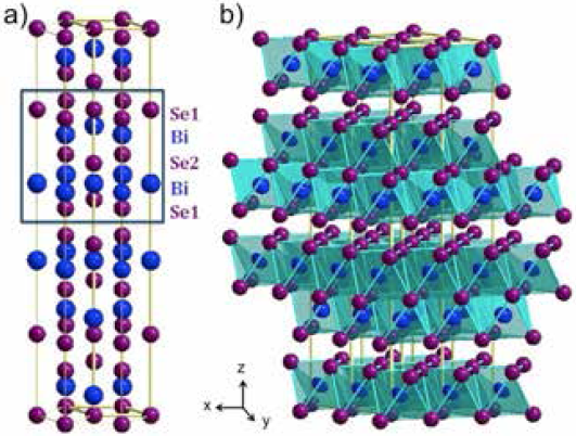
Fig. 1 a) Crystal structure of Bi2Se3, consisting of stacked quintuple layers, in the order Se1-Bi-Se2-Bi-Se1. b) Double layers of BiSe6 octahedra.
Bi2Se3 may accept many chemical modifications, either by Bi substitution, as in Bi2-x-ySbxPbySe3[15]; or by Se substitution, as in Bi2Se3-Bi2Te3, forming a solid solution [13]. Intercalation between the double-layers is also possible and it has been recently reported that doping bismuth selenide with small amounts of copper, CuxBi2Se3, results in a superconducting compound [16-18].
In order to elucidate the role that higher doping concentration has on the structure of Bi2Se3 and its effect on the superconducting and thermoelectric properties we have prepared CuxBi2Se3 with x = 0.11 to 0.20 we present chemical and structural characterization, and the electronic properties of CuxBi2Se3. Superconductivity was characterized via magnetization and resistivity measurements as a function of temperature. The chemical environment of the atoms was probed with X-ray photoelectron spectroscopy for the different compositions.
Results and Discussion
Samples were prepared as described in the experimental section. The crystal structure was confirmed by X-ray diffraction (Fig. 2), identified by comparison with X-ray patterns of rhombohedral Bi2Se3 in the Inorganic Crystal Structure Database (ICSD: 04-2545). The obtained patterns show that the crystals are single phase and the sharp reflections indicate their high crystallinity. These reflections correspond to the basal plane (00l), obeying the expected systematic absences for the R-3m rhombohedral space group and the total preferred orientation of the platelet-like crystals. Le Bail fits to the diffraction data confirm the Cu insertion with an increase of the c-axis from c = 28.6495(6) Å, for Bi2Se3 to c = 28.7100(7) Å, for Cu0.20Bi2Se3. The shift of the cell parameter suggests that for high doping levels inter and intra-layer Cu susbtitution is taking place in CuxBi2Se3. The Cu atoms are incorporated either by Bi substitution or by intercalation between the double-layers. In the case of Bi substitution the lattice constant would be smaller due to smaller Cu+ ion radius (0.77 Å, Bi3+ radii = 1.03 Å). In the case of intercalation between the double-layers there should be an increase in the c-axis lattice constant.
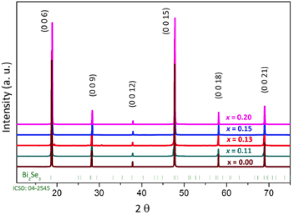
Fig. 2 X-ray diffraction patterns of cleaved single crystals of CuxBi2Se3 at various Cu concentrations.
The crystal structure can be seen as alternating layers of bismuth and selenium along the c direction. The unit cell has three hexagonal “quintuple” layers. The stacking in each quintuple layer occurs in Se1-Bi1-Se2-Bi1-Se1 order, where 1 and 2 refers to different atomic positions as indicated in Fig. 1. Se1 and Bi1 are located on the 6c site, (0, 0, z), (z = 0.2115 and 0.3985 respectively), and Se2 on the 3a site, (0, 0, 0) [19]. The chemical bonding intra-quintuple-layer has been shown to be covalent, while the bonding inter-quintuple-layer is weak predominantly by van der Waals interactions [13, 20]. These crystal properties make an easy-to-cleavage material due to its layered nature.
In order to study the surface morphology, scanning electron microscopy (SEM) and energy-dispersive X-ray spectroscopy (EDS) were performed on the different chemical phases and composition.
The back scattering electron (BSE) images show homogeneity in the samples; no segregation or clusters of the dopant were found (Fig. 3a and 3c). As mentioned above the structures are layered due to the crystallographic nature of the bismuth chalcogenides. The EDS spectra indicate that Bi, Se and Cu are the only elements present in the samples, Fig. 3b and 3d.
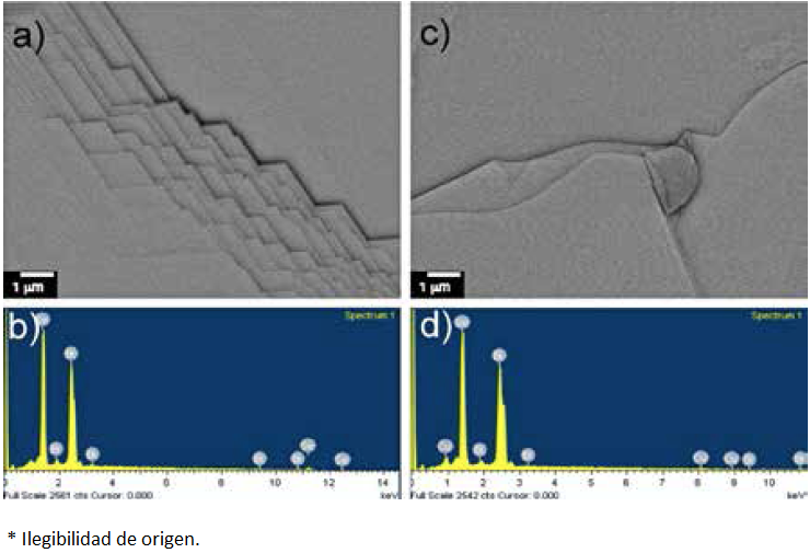
Fig. 3 Backscattered electron images and energy-dispersive X-ray spectroscopy performed on a) and b) Bi2Se3 and c) and d) Cu0.13Bi2Se3, respectively.
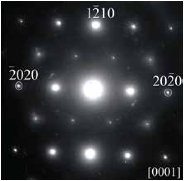
Moreover, to confirm any possible superstructure, electron diffraction microscopy was performed. The sample preparation consisted of mechanical exfoliation, in a “graphene-like” manner. The selected area electron diffraction (SAED) pattern shown in Fig. 4 was taken from the Cu0.15Bi2Se3 sample, but is representative of all the series. The diffraction pattern is characteristic of a single domain and no diffuse scattering or extra maxima were observed, in contrast with CuxTiSe2 where the Cu orders in between the layers doubling the a and c parameters [21]. The pattern can be identified as the [0 0 1] zone axis projection of the hexagonal Bi2Se3 reciprocal lattice.
The X-ray photoelectron spectroscopy analyses are shown in Fig. 5, the XPS survey spectra were taken after etching samples for 5 min with Ar+. It is observed that after etching the surface is free of carbon and oxygen. The doped samples also show the characteristic binding energies for Cu orbitals, indicating that all of them have copper inside.
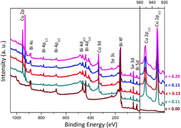
Fig. 5 X-ray photoelectron spectroscopy spectra of CuxBi2Se3 samples. Right side shows an enlargement of Cu 2p orbital.
To understand the role of chemical state via analysis of the binding energy (BE), we performed high-resolution XPS spectra core level for the Bi 4f, Bi 5d, Se 3d and Cu 2p orbitals, Fig. 6. The energy ranges corresponding to the Bi 4f and Bi 5d orbitals are shown in Fig. 6a and 6b, respectively. It is observed that the CuxBi2Se3 samples do not have Bi metal or Bi2O3 impurities; except for a small amount when x = 0.11, where the peaks show a broadening at lower energies indicating that Bi metal is present. The BE of Bi 5d 3/2 and Bi 5d 5/2 are 27.40 eV and 24.30 eV in Bi2Se3, respectively. It can be observed that there is a slight shift of the BE to lower energies for these orbitals with the insertion of copper in the samples; which could be explained if the incorporated copper atoms exist as Cu+ ions, in agreement with other reports [22, 23].

The binding energies for the Se 3d 3/2 and Se 3d 5/2 orbitals are very close, Fig. 6c. The binding energy ranges for the Cu 2p 1/2 and Cu 2p 3/2 orbitals, depicted in Fig. 6d, show that copper is present as copper ions Cu+ in all the doped samples.
The magnetic susceptibility 𝓧 of all the doped samples measured at 10 Oe in the temperature range from 2 to 8 K are shown in Fig. 7. These data show that all doped samples are superconducting, with a Tc onset of 3.4 K for x = 0.13, in agreement with other reports [16, 18, 23].
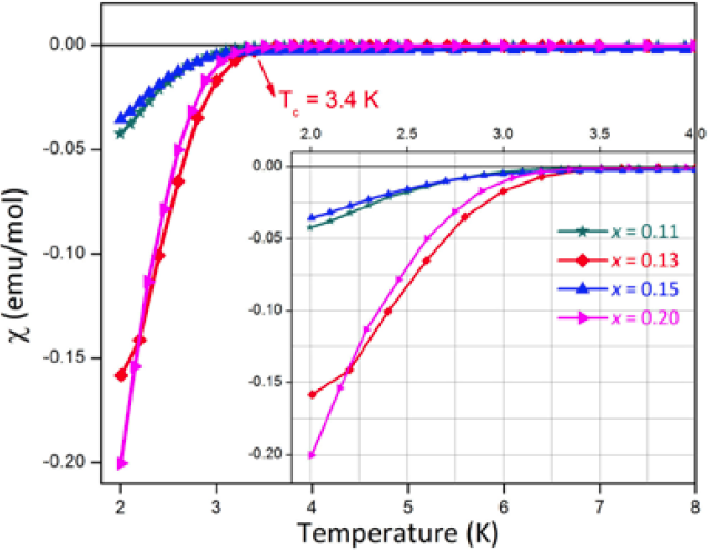
Fig. 7 Susceptibility as a function of temperature, from 2 to 8 K at an applied field H = 10 Oe. Note that the diamagnetic behavior indicates a Tc= 3.4 K. The inset shows a close view from 2 K to 4 K.
Resistance measurements were performed from 300 to 2 K. They show a metallic behavior (Fig. 8). The samples with composition x = 0.15 and x =0.20 show a drop in the resistance, at the same temperature where the diamagnetic behavior appears, but the resistance does not drop to zero, indicating that the amount of superconducting material is quite small and the percolation limit is not reached. This observation is indicative of no bulk superconductivity. The ratio of the resistance from room temperature to about 4 K is small.
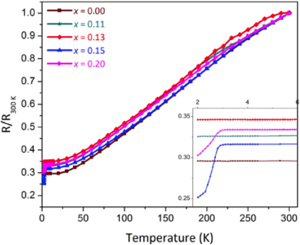
Fig. 8 Resistance measurements in the temperature range from 300 to 2K, normalized at 300 K. The inset shows the low temperature region where the drop in the resistance for x = 0.15 and x = 0.20 can be clearly observed.
In addition we performed thermoelectric properties measurements; Seebeck coefficient S, resistivity (ρ=1/σ), and thermal conductivity k. In order to obtain a good thermoelectric material it is necessary to have high values of S and σ, which implies a low resistivity value, and the lowest κ possible, resulting in a high ZT value. Therefore, we compare the thermoelectric properties of Cu0.15Bi2Se3, Cu0.20Bi2Se3 and Bi2Se3; Fig. 9 shows the differences between these compounds. These results show that when doping bismuth selenide with copper the Seebeck coefficient is diminished, the thermal conductivity decreases its value at low temperature (2 - 100 K) and the resistivity has no significant modification. Accordingly, the figure of merit drops down to zero in all the temperature range measured, resulting in a material with poor thermoelectric properties for applications in the temperature region studied. The apparent semiconductor behavior observed for x = 0.20 in resistivity data (Fig. 9a) is probably due to non-ohmic contact resistance. It is worth noting that in the analogue compound CuxBi2Te3, the thermoelectric properties are improved with the insertion of Cu nanoparticles [24], which is opposed to what we observed in CuxBi2Se3.
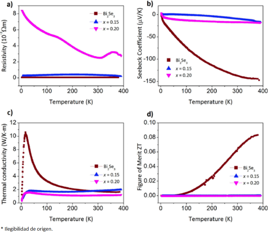
Fig. 9 Thermoelectric properties of Bi2Se3 and CuxBi2Se3, the measurements were recorded in the temperature range from 390 to 2 K.
Ideally, one would like to have independence between the electrical and the thermal transport, and that is the success on the use of layered compounds as thermoelectric materials, their structure favors this independence [25]. At first glance, copper doping on Bi2Se3 looks like a naive approach in order to reach a high ZT value, since its metallic character will increase both electrical and thermal transport. However, if Cu is just inserted (inter-quintuple-layer) and not substituted (intra-quintuple-layer), i.e. keeping an independence between ab-plane and c-axis, the electrical transport will be increased along the ab-plane but with a big anisotropy regarding the c-axis, and vice versa for the thermal transport. XPS results show a reduction on the Bi binding energy, which increases with Cu insertion; this is due to a change on the bismuth chemical environment (intra-quintuple-layer). Therefore, we propose that both intercalation and substitution are present in CuxBi2Se3, resulting in a decrement of the thermoelectric transport values as the Cu content increases.
Conclusions
In summary we have studied the system CuxBi2Se3 with x = 0.11 to 0.20. X-ray and electron diffraction confirm the crystallinity and crystallographic orientation of the compounds. SEM images show homogeneity in the surface morphology. The chemical analyses (XPS) indicate that Cu is present as Cu+ in doped Bi2Se3. Bi 4f and 5d orbitals, as well as Se 3d on the doped samples show a similar chemical environment as in Bi2Se3 sample, although there is a slight displacement on the Bi2Se3 binding energy of Bi and Se orbitals due to copper insertion.
Magnetization measurements indicate that all the doped compounds are superconductors with a Tc onset = 3.4 K. Nevertheless, the thermoelectric properties values are reduced due to copper intercalation. Chemical and electronic properties are modified by the incorporation of small amounts of Cu and suggest not only intercalation but also substitution on Bi2Se3.
Experimental
Stoichiometric amounts of high purity Bi (Sigma-Aldrich 99.999%), Se (Alfa Aesar 99.999%) and Cu (Sigma-Aldrich 99.99%) were ground together, pressed into pellets and sealed in evacuated quartz tubes. The sample was heated (9 h) to a maximum temperature of 850°C and held at that temperature for 24 h. After this procedure samples were slowly cooled to 630°C and annealed for 24 h. The last step of the synthesis was the quenching of the tubes into water at room temperature; this was needed for the copper intercalation to occur in between the double octahedral layers. Single crystals were obtained with a platelet-like shape.
The phase identification was done with an X-ray diffractometer Bruker D8 using Cu-Kα1 (λ = 1.5406 Å) radiation with a Ni filter, under operating conditions of 30 keV and 30 mA, in a Bragg-Brentano geometry. Surface morphology studies were performed with a scanning electron microscope FEG JEOL-7600F at 15 keV of accelerating voltage equipped with X-ray energy dispersive analyzer Oxford INCA X-Act. Selected-area electron diffraction (SAED) patterns were obtained in a transmission electron microscope JEOL JEM-1200EX operated at an accelerating voltage of 120 keV. X-ray photoelectron spectroscopy analyses were performed in an ultra high vacuum (UHV) system VG-Scientific Microtech Multilab ESCA2000, with Mg Kα X-ray source (hn = 1253.6 eV), and a CLAM4 MCD analyzer. The surface of the samples were etched for 5 min with 3.0 kV Ar+ at 0.10 μA mm-2. The XPS spectra were obtained at 55° to the normal surface in the constant pass energy mode (CAE), E0= 50 and 20 eV for surface and high resolution narrow scan, respectively. The peak positions were referenced to the background silver 3d 5/2 photopeak at 368.20 eV, having a FWHM of 1.00 eV, and C 1s hydrocarbon groups in 284.50 eV central peak core level position. The XPS spectra were fitted using the SDP v 4.1 program [26]. The XPS error was based on a detection limit estimated to be 0.1%. For the deconvolution analyses the estimated error was 5% (i.e. ±0.05 eV) of uncertain propagation.
Electrical transport and figure of merit measurements were performed in a commercial physical properties measurement system (PPMS, Quantum Design) in the 300 - 2 K temperature range. Magnetization measurements were done using a SQUID based magnetometer (MPMS, Quantum Design) from 2 to 8 K with an applied magnetic field of 10 Oe.

