


 text new page (beta)
 English (pdf)
 Article in xml format
 Article references
 Send this article by e-mail
 Cited by SciELO
  Similars in
SciELO
Similars in
SciELO 
 Permalink
1. Introduction
In recent advancements, DC-DC power electronic boost converters have had a significant role in various applications such as hybrid electric vehicles, fuel cell energy conversion systems, medical equipment, military applications, battery charging and many more, where the high DC output voltage is obtained with the high ON time of the power switches. However, the high ON time (high duty cycle) led to certain issues such as reduced efficiency of power conversion, high potential stress across the switches, severe reverse-recovery issue of diodes, and electromagnetic interference problems (Hsieh, Chen, Liang, & Yang, 2012; Yang, Liang, & Chen, 2009). The conventional boost converters may be cascaded to increase the DC output voltage level with low value duty cycle operation (Prabhala, Fajri, Gouribhatla, Baddipadiga, & Ferdowsi, 2016; Wai, Lin, Duan, & Chang, 2007). While cascading, the efficiency of power conversion gets decreased. Another disadvantage is that the increased potential stress appearing across the power switch and the diode at the output stage. A single switch-based concept of cascading two boost converters was used in the quadratic converter. But this type of converter employed inductor and capacitor of higher ratings and suffers from the high potential switch stress. Several stacked converters are introduced by some authors to increase the voltage gain (Dwari & Parsa, 2011; Wu, Chen, Yang, & Kuo, 2010). However, these types of converters also suffer from the disadvantage that the capacitors at the output need to maintain voltage balance across them particularly when their number is increased. The voltage stress appearing across the output diode of the conventional boost converter can be mitigated using three levels in the conventional converter and the increase in effective frequency can reduce the size of inductors (Yaramasu & Wu, 2011). This converter is impracticable for certain applications due to the insufficient voltage level at the output.
There are certain types of isolated power electronic converters which utilize the concept of adjusting the number of turns on the primary and secondary side of the transformer to obtain the increased output voltage levels. However, the high leakage inductance of the transformer and increased potential switch stress limit the applications of these converters. Some authors developed certain converter configurations that are able to produce high DC output voltage, high power conversion efficiency and reduced switch stress by utilizing magnetically coupled inductor along with transformer (Duarte et al., 2013; Evran & Aydemir, 2014; Forouzesh, Siwakoti, Gorji, Blaabjerg, & Lehman, 2017; Tofoli, de Castro Pereira, de Paula, & Júnior, 2015). But many converter topologies that can improve both the voltage gain and efficiency are presented in the literature (Chub, Vinnikov, Blaabjerg, & Peng, 2016; He & Khaligh, 2017; Hu & Gong, 2014; Tseng & Huang, 2014).
It is also possible to reduce the switch stress along with improved output voltage level if voltage multiplier cells are hybridized with the conventional single switch power converters. The conventional, Cuk and SEPIC DC-DC converters employ voltage multiplier circuitry (Chub et al., 2016). The conventional step-up converter’s gain may be increased N times by a power electronic converter which is capable to produce inverting DC output voltage (Mahajan, Sanjeevikumar, Ojo, Rivera, & Kulkarni, 2016). Further, there are power converters that employ interleaved boost concept to increase the DC output voltage level with reduced ripples in the output voltage and output current (Bhaskar, Kulkarni, Padmanaban, Siano, & Blaabjerg, 2016). Some authors proposed the concept of interleaved multilevel voltage multiplier-based power converter topologies that are capable to produce 2N and 4N times the output voltage level of conventional boost topology (Bhaskar, Sanjeevikumar, et al., 2016). But, this high output voltage level is influenced by (i). balancing of voltages across the various capacitors with suitable time constants, and (ii). more number of diodes. The charge and discharge characteristics of the capacitors influence the power conversion efficiency (Bhaskar, et al., 2016). Two or more conventional boost converters can be connected in parallel using interleaving technique. This interleaving technology can easily cause the filtering of ripples in the input current (Li & He, 2011; O’Loughlin, 2006; Roy & Ayyanar, 2017). The range of DC output voltage can be increased using coupled inductors along with voltage multiplier units (Rosas-Caro et al., 2011). However, while using coupled inductors concept, energy circulation and snubber circuits are required to reduce the potential stress across the switches.
Switched capacitor (SC)-based converters, having high efficiency with good output voltage regulation and low weight, mainly consist of large number of switching devices and capacitors with various ratings, and the output voltage level can be boosted by the charge and discharge characteristics of capacitors (Mahajan, Sanjeevikumar, & Blaabjerg, 2017; Qian et al., 2012). The use of large number of switching devices leads to high switching losses. Hence, the efficiency of the SC-based DC-DC converter cannot be improved due to large power rating of the switching devices. Moreover, the increase of voltage gain of the converter is also limited. The SC-based converter circuits can have higher energy and power densities since they do not use reactive elements for energy transfer. Moreover, the SC circuit can be fabricated into an integrated chip (IC) and mostly used in low-power electronics applications.
There is another possible solution for improving the DC voltage gain of the converter using switched inductor (SI)-based DC-DC conversion technology, which employs parallel-charge and series-discharge inductors (Yang et al., 2009; Gautam, Sharma, & Shukla, 2019). This switched inductor-based converter configuration can operate in boost mode as well as in buck-boost mode. When it is operated in boost mode, then the configuration is called switched inductor boost converter (SI-BC), and in buck-boost mode, it is called switched inductor buck boost converter (SI-BBC). These configurations employ only a single active switch. But the switch is subjected to high voltage stress. Both the SI-BC and SI-BBC configurations are capable to improve the voltage gain by (1+Duty ratio) times and two times compared to the respective conventional DC-DC converters.
Some authors proposed a high step-up DC-DC converter structure consisting of a full-bridge module and the Cockcroft-Walton principle-based voltage multiplier to achieve high voltage gain in photovoltaic applications (Hossain, Selvaraj, & Rahim, 2018). A quasi-switched boost inverter configuration with voltage multiplier cell can be used for achieving high voltage gain with decreased voltage stress on the switches (Nguyen & Chai, 2019). A non-isolated approach of LLC resonant DC-DC converter with balanced rectifying current and stress has been proposed by some authors (Dobi & Sahid, 2020). This configuration has significantly reduced transformer loss because of non-isolation. The PI controller-based super lift technique applied to DC-DC Luo converters has been proposed by some authors to improve the voltage conversion ratio (Adlakha, Khosla, & Joshi, 2020) in which the comparative analysis of various positive output super lift DC-DC Luo converters is discussed. A non-isolated high voltage gain DC-DC converter proposed in (Saravanan & Ramesh Babu, 2019) is compared with boost, SEPIC and modified SEPIC converters. The converter proposed in (Saravanan et al., 2019) shows high efficiency compared to the other converters.
In this work, a diode rectifier-fed positive output power electronic converter, capable to increase the DC output voltage to the higher level without using high duty ratio of the switches, is analyzed theoretically and using simulation software. Here, three identical inductors each of value 0.1 mH are used. The concept of parallel-charge and series-discharge characteristics of the switched inductors is used to increase the DC output voltage level to the higher value. It employs only two power semiconductor switches which are subjected to low voltage and current stresses during the switch-off and switch-on periods. There are certain assumptions to be made for the analysis of the proposed converter:
The diodes and MOSFETs used in the converter have negligible forward voltage drops and are having negligible resistance during forward conduction mode. The inductors and capacitors used are lossless.
Large capacitances are assumed for the capacitors to maintain constant voltages across them.
The current flow through the three inductors in the proposed configuration increases or decreases linearly.
The remaining sections are arranged in such a way that the proposed work is illustrated effectively. The section 2 describes the configuration and various modes of operation of the converter under study. The MATLAB / SIMULINK model of the converter and its time domain simulation results are discussed in section 3. The conclusion for the proposed work is given in section 4.
2. Configuration and modes of operation of the converter under study
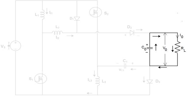
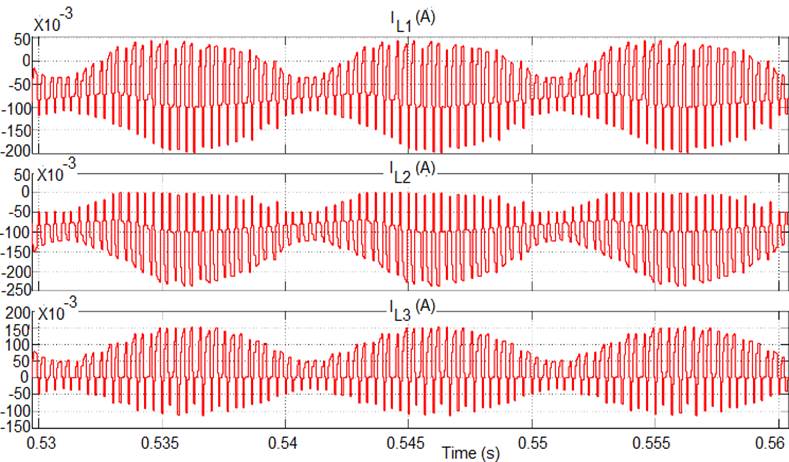
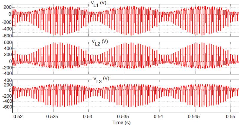
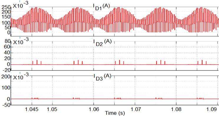
The topology of a rectifier-fed non-isolated high step-up positive output converter capable of producing high DC output voltage is shown in Figure 1. The single-phase AC supply of 50 Hz frequency is fed to a diode bridge rectifier which gives an uncontrolled DC voltage. The ripples in the DC voltage are filtered by a capacitor. The filtered DC output voltage is acting as source to the DC-DC converter stage whose output is filtered by a capacitor C 0. The converter output voltage appears across a load R L . The proposed converter employs three identical inductors of inductances L 1, L 2 and L 3 respectively. The two high power semiconductor switches S 1 and S 2 are triggered simultaneously into conduction by proper gate signals. The theoretical waveforms of the rectifier-fed converter operating under continuous and discontinuous inductor currents are presented in Figure 2. Both the continuous and discontinuous modes of operations of the converter are discussed. In this work, the simulation of the proposed converter is carried out under continuous inductor current mode. The various modes of operation of the converter under continuous and discontinuous inductor current modes are explained as shown below:
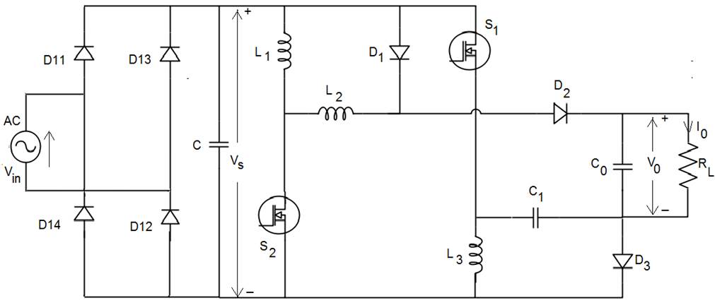
Figure 1 Circuit configuration of the proposed rectifier-fed non-isolated positive output DC-DC boost converter.
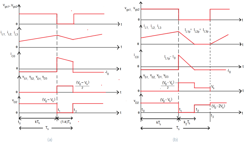
Figure 2 Theoretical waveforms of the converter under study during (a). continuous inductor current mode, and (b). discontinuous inductor current mode.
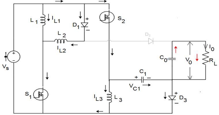
2.1. Mode-I operation of the converter during the time interval t0-t1
2.1.1. Steady-state analysis:
Both the high power semiconductor switches S
1 and S
2, of the converter under continuous inductor current mode /
discontinuous inductor current mode, are switched on during the time
interval
Thus, the three identical inductors and the capacitor
2.1.2. State-space analysis:
The dynamic and output equations of the circuit for the ON period of the switches S 1 and S 2 are obtained as follows:
By applying Kirchhoff’s Voltage Law to the circuit shown in Figure 3, we get
Since all the three identical inductors carry equal currents,
Eqn.(2) can be written as:
By applying Kirchhoff’s Current Law to the circuit shown in Figure 3, we get
From Eqns (2.b) and (3.a), the state-space model of the proposed converter during ON period is written as Eqns. (4.a) and (4.b):
2.2. Mode-II operation of the converter during the time interval t1 - t2:
2.2.1 Steady-state analysis:
Both the high power semiconductor switches
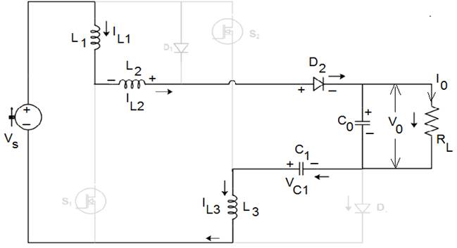
From the Figure 4, it is understood that all the three identical inductors carry the same current. Hence, they have the equal voltage drop of V s across them.
Therefore,
The Inductor Volt-Second Balance (IVSB) principle states that for steady state operation of an inductor in a DC-DC converter, the net inductor voltage in a switching period must be zero. By referring Figure 2, the following Eqn. (7) is obtained by applying the IVSB principle on the inductors L 1, L2 and L 3:
Finally, the voltage gain
2.2.2. State-space analysis:
The dynamic and output equations of the circuit for the OFF period of the
switches
By applying Kirchhoff’s Voltage Law to the circuit shown in Figure 4, we get
By applying Kirchhoff’s Current Law to the circuit shown in Figure 4, we get
From Eqns (9.b) and (10.b), the state-space model of the proposed converter during OFF period is written as Eqns. (11.a) and:
2.3. Mode-III operation of the converter during the time interval t2 - t3:
Both the active switches
3. MATLAB / SIMULINK model of the converter under study and its time-domain simulation results
The Simulink model of the rectifier-fed non-isolated positive output converter is
developed as shown in Figure 6 and the
converter operating under continuous inductor current mode is simulated in
Matlab/Simulink environment at a switching frequency of 3 kHz. Table 1 lists the values of circuit components
used for simulation. Table 1 also lists the
specifications of the converter under study. The converter circuit is simulated
using solver ‘ode 45’ of variable-step type. A graphical user interface (GUI) is
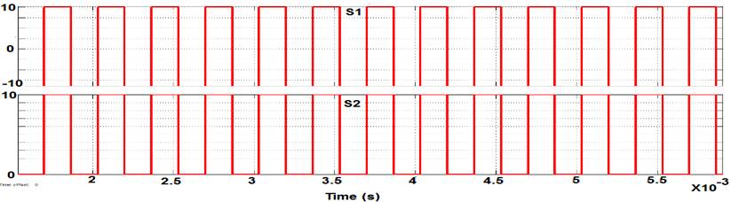
utilized by the simulink for solving process related simulations. The gating signals
given to the active switches
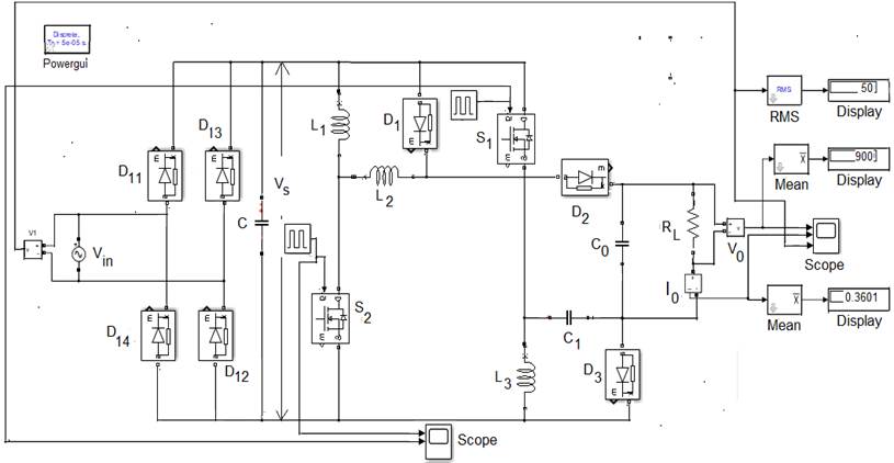
Table 1 Simulation parameters of the proposed converter.
| Parameters | Symbol | Value |
|---|---|---|
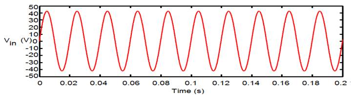
| Input Voltage | Vin | 30 V (rms) |
| Rectifier output voltage | V s | 90 V (Average DC) |
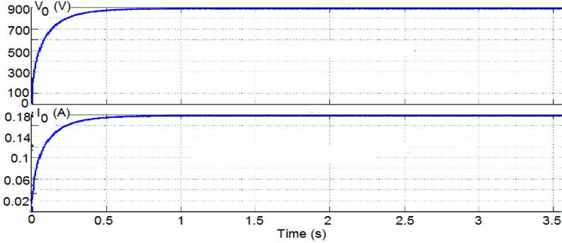
| Output Voltage | V o | 900 V (DC) |
| Inductors | L 1 , L 2 , L 3 | 0.1 mH each |
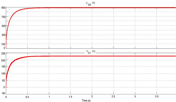
| Capacitors | C, C 1, C 0 | 100 µF, 360 µF, 280 µF |
| Switching frequency | F s | 3 kHz |
| Load Resistance | R L | 5 kW |
| Load power | P o | 160 W |
| Average output current | i o | 0.18 A |
| Duty ratio of the switches | k | 0.6 |
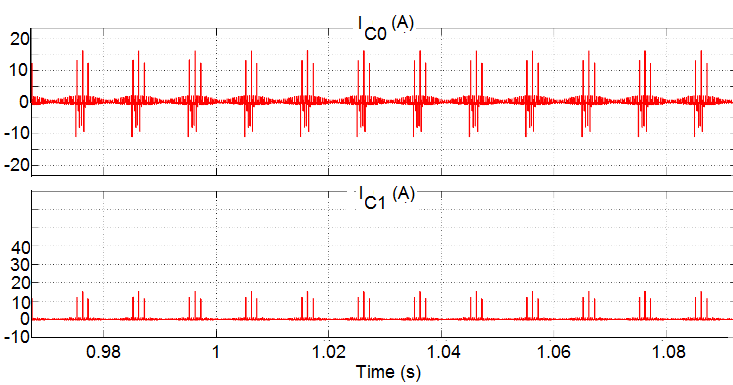
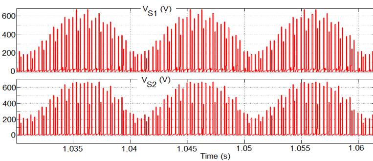
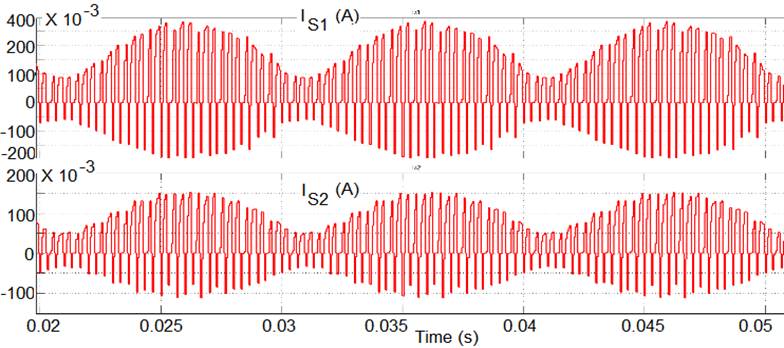
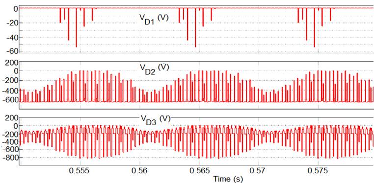
4. Conclusion
In this article, the open-loop implementation of a rectifier-fed non-isolated positive output high step-up gain power electronic converter has been proposed. The high output voltage level is obtained by a parallel-charge and series-discharge inductor-based voltage boosting technique. The principle of operation and steady state analysis of the proposed converter under continuous inductor current mode operation is analyzed. Both the steady state analysis and state-space analysis of the suggested converter are carried out. The performance of the rectifier-fed DC-DC converter is validated through the time-domain simulations carried out in Matlab/Simulink platform. The results demonstrate that the rectifier-fed converter configuration proposed in this work has the capability to produce an output DC voltage of around 900 V which is almost ten times the average input DC voltage. This improved output voltage level is obtained at extremely low duty ratio of the active switches. The output voltage and output current waveforms are characterized by significantly reduced overshoot and settling time. The voltages across and the currents through the non-dissipative elements in the converter configuration are also analyzed. The proposed converter configuration employs only two high power semiconductor switches (MOSFETs). There is a considerable reduction in the voltage and current stresses for the MOSFETs. The proposed step-up converter may find applications in many real time applications such as battery backup for uninterruptible power supplies, solar cell energy conversion system, automobiles, micro-ovens, and X-ray machines and CT scanners.

