


 text new page (beta)
 English (pdf)
 Article in xml format
 Article references
 Send this article by e-mail
 Cited by SciELO
  Similars in
SciELO
Similars in
SciELO 
 Permalink
Introducción
The infrared (IR) spectral region is of enormous interest as the manufacturing of optoelectronic devices operating in the 1.7-5.6 μm wavelength range offers potential applications in a wide variety of areas. These applications include optical gas sensing and environmental monitoring, free-space optical communications, infrared countermeasures, clean energy generation, biomedical and thermal imaging [1]. Various materials such as HgCdTe [2], and PbSnTe [3] are commercially applied to mid-infrared optoelectronics. However, drawbacks like high thermal coefficients and dielectric constant result in high diode capacitance and therefore limited frequency response, for PbTe, and difficulties in growing HgCdTe material due to solidus-liquidus separation and the high vapor pressure of Hg, encourage the development of alternative materials as the antimonide-based family [4].
IR wavelengths are readily accessible using antimonide-based semiconductors. This family of materials refers to III-V zinc blende alloys approximately lattice-matched to GaSb (with a lattice constant of 6.0959 Å) [5]. GaSb can accommodate various III-V binaries (InAs and InSb) as well as their ternary (InAsxSb1-x and GaInxSb1-x) [6], quaternary (InxGa1-xAsySb1-y) [7], and quinary alloys (AlxGayIn1-x-yAszSb1-z) [8]. This allows for a diverse range of band alignments. The versatility of the GaSb-based material system makes a broad spectrum of wavelengths accessible. Among the Sb-based semiconductors, the InxGa1-xAsySb1-y alloy has demonstrated to be an alternative to the use of alloys such as those formed by the HgCdTe. This is due to the fact that the adjustment of the compositions allows a wide bandgap range, from 0.36 to 0.80 eV and maintains the lattice parameter matched to the GaSb substrate [9]. This wide range has an important role in the manufacture of IR devices such as diode laser [10], photodetectors [11], and thermophotovoltaic cells [12].
Due to the technological interest in InxGa1-xAsySb1-y alloys, different growth techniques have been developed to obtain this semiconductor. InxGa1-xAsySb1-y alloy single crystals can be grown by liquid-phase epitaxy (LPE) [13], metalorganic vapor-phase epitaxy (MOVPE) [14], and molecular-beam epitaxy (MBE) [15]. LPE is a low-cost manufacturing technique that usually operates close to the thermodynamic equilibrium, while MOVPE and MBE occur quite far from equilibrium, and with higher operating costs. LPE is the simplest and the cheapest way to grow layers with flat surfaces in homoepitaxy and near lattice-matched in heteroepitaxy [16,17]. The growth is performed from a supersaturated liquid solution or a melt on a substrate. The supersaturation is obtained by cooling the solution from the thermodynamic equilibrium. It drives the growth of the layer, and it can be generated by the following methods, ramp-cooling, step-cooling, super-cooling, or transient growth [18,19].
LPE enables the growth of crystalline layers with an extraordinarily high structural quality and growth rates (1 μm/min), a wide selection of dopants, suppression of certain types of defects, and absence of highly toxic precursors [20]. A basic requirement is the phase diagram that once it is established [17,21], growths can occur over a wide range of temperatures. Since growth conditions of the LPE processes are close to thermodynamic equilibrium, atoms can efficiently migrate to the growth interface and find optimal positions for incorporation. This may result in crystalline layers with a very low density of point and dislocation defects. Compound semiconductor layers grown by LPE exhibited point defects densities orders of magnitudes lower than layers grown by other growth techniques. The carrier lifetime in such layers is consequently quite high [19]. In addition, controlling the As and In contents has an important role in the epitaxial growth of InxGa1-xAsySb1-y alloys with low lattice mismatch.
In this research, InxGa1-xAsySb1-y alloys were grown on GaSb(100) substrates by liquid phase epitaxy using the ramp-cooling method. The purpose of growing this quaternary layer is to analyze its crystalline quality, interface quality, superficial roughness, plasmon-phonon interaction, and radiative transitions in a near-lattice-matched epitaxial growth on GaSb substrates by LPE technique, to subsequently apply it in IR optoelectronic devices. High-resolution X-ray Diffraction (HR-XRD), Raman spectroscopy, Scanning Transmission Electron Microscopy (STEM), Atomic Force Microscopy (AFM), Secondary-Ion Mass Spectrometry (SIMS) and Photoluminescence (PL) were the techniques used in this study.
Experimental Details
In x Ga 1-x As y Sb 1-y on GaSb substrates by LPE technique
Samples of InxGa1-xAsySb1-y layers with In content x = 0.145, and As content y = 0.132 on top of GaSb(100) substrates were grown using the LPE technique. The substrates were single crystal wafers, which were chemically cleaned, while the melts for the In0.145Ga0.855As0.132Sb0.868 layers were prepared using 6N purity sources of In, Sb and Ga, and pieces of GaAs wafers as the As source. The growth by LPE was carried out in a horizontal furnace system, where a graphite sliding-boat acts as a reactor, under a palladium-purified hydrogen atmosphere. The reactor was placed inside a sealed quartz tube. Figure 1 shows the quaternary film growth curve, where the system temperature is a function of the growth process time. The process begins by placing the previously cleansed substrates into the reactor and the components which constitute the melt. Once the system is closed and presents no gas leaks, the system temperature is raised up to 640 °C, in order to remove oxides (chemical desorption) from the substrates. After that, the temperature drops at a rate of 3.5 °C/min to the thermodynamic equilibrium temperature at 536 °C, where it remains for about 2 hours with the intention of having no thermal variations related to the furnace. Subsequently, the under-

Figure 1 Temperature diagram for the growth of In0.145Ga0.855As0.132Sb0.868 layers as a function of time.
cooling process takes place by using a cooling ramp at a rate of 0.3 °C/min. The quaternary alloys were grown when the system reached 529 °C, at which point the substrate was kept in contact with the melt for one minute. These were the optimal growth conditions used to obtain In0.145Ga0.855As0.132Sb0.868/GaSb layers with low lattice mismatch.
Structural characterization
High Resolution X-Ray Diffraction (HR-XRD) spectra measurements were made in a Panalytical MRD X-ray diffractometer with a Kα1 emission line from a Cu target as an X-ray source. 2-bounce hybrid monochromator and 3 bounce analyzer manufactured of Germanium (200) were used. The first, to remove the contribution of Kα2, and the second, to reach the maximum resolution. Raman spectra were obtained with a laser confocal Raman spectrometer (NT-MDT, Integra Spectra) recorded at room temperature in the backscattering geometry. Spectra were measured by using a laser wavelength of 473, 532 and 633 nm at normal incidence. The beams were focused to a diameter of 6 µm at the sample with an aperture microscope objective of 100 µm. The aberration-corrected scanning transmission electron microscopy (AC-STEM) micrographs were obtained in a JEOL-ARM200F at 200 kV. The sample was prepared by a standard focused ion beam procedure.
Morphological characterization
Morphology images were obtained with an Atomic Force Microscope (AFM) in a ThermoMicroscope equipped with a laser wavelength of 633 nm and operated in the tapping mode with an etched Si cantilever.
Chemical characterization
The SIMS profiling analysis was performed using a time-of-flight secondary ion-mass spectrometer (TOF-SIMS). For which, an area of 300 × 300 µm2 was sputtered, using a Cesium (Cs+) primary ion beam, with an energy of 0.5 keV. To study the In0.145Ga0.855As0.132Sb0.868/GaSb layers a secondary Bi3+M+ ions (M is the interest element) on an area of 100 × 100 µm2 were used.
Optical characterization
The optical properties of the quaternary alloys were characterized using low temperature photoluminescence spectroscopy. Measurements were carried out using a standard configuration equipped with an Acton monochromator and a closed-circuit Helium (He) refrigerator at 21 K. A 488 nm Ar+-ion laser supplied the optical excitation, and an InSb infrared detector EG&G Judson cooled with liquid nitrogen was used to detect the PL signal.
Results and discussion
A successful identification of the In0.145Ga0.855As0.132Sb0.868 epilayer and the GaSb substrate was performed by HR-XRD measurements, as shown in Figure 2. The
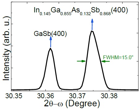
Figure 2 High-resolution X-ray diffraction
By using Bragg´s law, lattice parameters of a = 6.0934 Å, and a = 6.0959 Å, were determined for the In0.145Ga0.855As0.132Sb0.868 quaternary layer and the GaSb substrate, respectively. The lattice mismatch
The In0.145Ga0.855As0.132Sb0.868/GaSb stable atomic arrangement heterostructure was measured by Raman scattering using a laser excitation wavelength of 532 nm, as shown in Figure 3. Two peaks centered at 230 cm-1 and 244 cm-1 generated by the (GaSb-InAs)-like TO and the (GaSb-InAs)-like LO modes, respectively, proceed from the combination between the GaSb-InAs modes[22,23]. This indicates that the quaternary layer is mainly formed by the GaSb and InAs binary configurations, as X-ray Photoelectron Spectroscopy (XPS) measurements demonstrated by Casallas-Moreno et al. [7]. These two atomic arrangements exert less strain on the quaternary lattice due to their similar bond lengths (
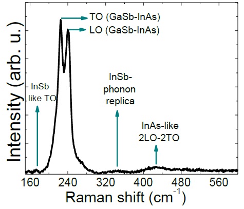
Figure 3 Raman spectrum for the In0.145Ga0.855As0.132Sb0.868/GaSb(100) layer, measured with an excitation wavelength of 532 nm.
Figure 4 shows Raman spectra of In0.145Ga0.855As0.132Sb0.868 sample measured with wavelengths of 473, 532 and 633 nm. Penetration depths of these wavelengths on this specific sample are 20, 35 and 150 nm, respectively, and were calculated by an extrapolation of the absorption coefficient of binary compounds [7].
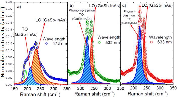
Figure 4 Multiwavelenght Raman spectra for the In0.145Ga0.855As0.132Sb0.868/GaSb(100); measured with excitation wavelengths a) 473, b) 532, and c) 633 nm.
Raman spectra were normalized to the integrated area in such a way that it is possible to observe the relative changes of diverse phonon modes in the total signal as a function of wavelengths. Figure 4a shows the Raman spectrum measured at 473 nm whose convoluted signal is originated by the GaSb-InAs LO-like and GaSb-InAs TO-like modes located at 230 and 244 cm-1, respectively, as previously described. The little signal located at 198 cm-1 is caused by the InSb LO mode. In the spectrum of Figure 4b measured at 532 nm it looks the same GaSb-InAs LO-like mode at 244 cm-1, however, the Raman signal increases its intensity at the TO frequency with respect to the signal shown in Figure 4a. This effect is originated by the fact that 532 nm laser wavelength increases its penetration depth with respect to 473 nm, and it is possible to excite plasmons in the bulk region by phonon-plasmon coupling, which is not significantly observable at 473 nm. The spectrum measured with 633 nm laser wavelength (Figure 4c) shows a greater intensity of the phonon-plasmon coupling than observed at lower wavelengths. This supports the idea of that as excitation wavelengths increases a major volumetric density of plasmon-phonon interaction can be reached. Additionally, it can be observed that as measure wavelengths increase the FWHM decreases for all LO, TO and phonon-plasmon deconvoluted signals. This evidence that crystalline quality increases at greater depth in the sample with respect to the surface.
The existence of plasmons in the bulk region indicates a high crystalline quality of these quaternary alloys and the evolution of the integrated intensity as a function of wavelength allows to identify the features of the depletion zone and the interface quality. Figure 5a shows the cross-sectional High Angle Annular Dark-Field (HAADF) micrograph of the In0.145Ga0.855As0.132Sb0.868/GaSb(100) heterostructure obtained with an Aberration-Corrected Scanning Transmission Electron Microscope (AC-STEM).
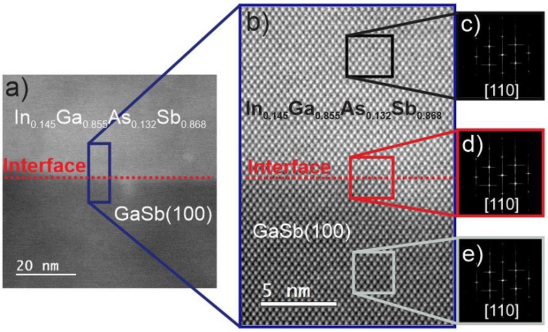
Figure 5 Cross-sectional HAADF micrograph of a) In0.145Ga0.855As0.132Sb0.868 layer grown on GaSb(100) substrate by LPE, and of b) the atomic lattice for each section of the sample; In0.145Ga0.855As0.132Sb0.868 layer, In0.145Ga0.855As0.132Sb0.868/GaSb interface and GaSb substrate. c), d) and e) illustrate the FFT patterns obtained in each region.
The interface is indicated by a red-dotted line. An abrupt interface is observed between the In0.145Ga0.855As0.132Sb0.868 quaternary layer and the substrate. Figure 5b presents the cross-sectional HAADF micrograph amplifying the area of each layer of the sample; In0.145Ga0.855As0.132Sb0.868 layer, In0.145Ga0.855As0.132Sb0.868/GaSb interface, and GaSb substrate. The same atomic arrangement between the quaternary layer and substrate is observed without linear defects such as dislocations or planar defects as stacking faults. This micrograph was processed through the Fast Fourier Transform (FFT) by Digital Micrograph software to obtain the diffraction patterns of the quaternary layer, In0.145Ga0.855As0.132Sb0.868/ GaSb interface, and substrate, as shown in Figure 5 (c, d, and e), respectively. Comparing the patterns, they consist of round spots with the same disposition and coherence, which means that the In0.145Ga0.855As0.132Sb0.868 layer has the same orientation as the GaSb(100) substrate. From the diffraction patterns of the quaternary layer (Figure 5c) and the GaSb substrate (Figure 5e), the lattice parameter is obtained for layer and substrate. The calculated constant was
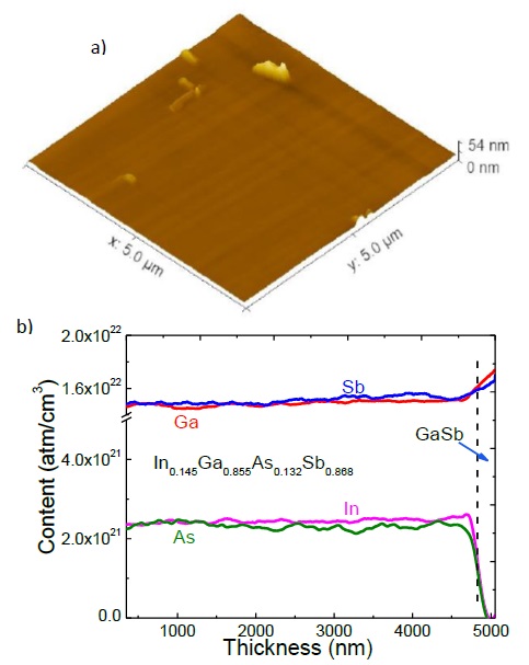
Figure 6 a) AFM image of the In0.145Ga0.855As0.132Sb0.868 layer grown on a GaSb(100) substrate. b) SIMS depth profile of the In0.145Ga0.855As0.132Sb0.868 layer grown on GaSb(100) substrate.
The chemical depth profile of the In0.145Ga0.855As0.132Sb0.868 layer on a GaSb substrate was obtained by SIMS technique, as shown in Figure 6b. This profile shows a uniform distribution of the atomic elements (Ga, In, As, and Sb) along the quaternary layer demonstrating the high crystalline quality found by HR-XRD, and the low RMS roughness pointed out by AFM. In addition, an abrupt interface between the In0.145Ga0.855As0.132Sb0.868 layer and the GaSb substrate was observed; this means that there is a through the interface layer/substrate. Figure 7 shows the photoluminescence spectrum of the In0.145Ga0.855As0.132Sb0.868 layer at 21K. The spectrum presents two peaks located at 641 and 637 meV attributed to radiative transitions [7] due to the recombination of bound exciton states (BE) and radiative recombination transitions involving donor-acceptor-pairs (DAP) from the native defect centers.
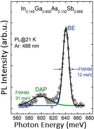
Figure 7 PL spectrum of the In0.145Ga0.855As0.132Sb0.868 layer growth on a GaSb(100) substrate measured at 21 K. Gaussian fitting for the BE and DAP transitions are represented by a blue and green solid lines, respectively.
The high intensity of the BE transition evidences the high crystalline quality of the grown layer, and this was confirmed by determining the FWHM. The FWHM is sensitive to crystalline imperfections, for example, the presence of misfit dislocations would result in a local sloping of lattice planes and a broadening of the peak [24]. The FWHM of the BE transition is ~12 meV, which means high crystal quality and low lattice mismatch as found by HR-XRD and AC-STEM, and as reported in the literature for InxGa1-xAsySb1-y films grown by LPE with similar stoichiometric [22], [25]. The DAP broadband presents a FWHM around of ~ 31 meV, the value is acceptable for this type of transitions [22]. Moreover, it was estimated the band gap energy for the In0.145Ga0.855As0.133Sb0.867 crystalline layer by adding approximately 4 meV [26] (that corresponds to the sum of the exciton dissociation energy and free exciton binding energy) to the energy of the BE excitonic transition obtained from PL measurements. Therefore, the band gap energy of the In0.145Ga0.855As0.132Sb0.868 layer is 635 meV (1.95 µm). In Figure 8, the band gap energy of the In0.145Ga0.855As0.132Sb0.868 crystalline layer experimentally obtained by PL measurement at 21 K is presented with the star on the calculated curves of the band gap energy as a function of lattice parameter for antimonides alloys, the curves have been obtained from the E(x,y) and a(x,y) relations [7], at 21 K. It is important to mention that the In x Ga 1-x As y Sb 1-y alloys lattice-matched to GaSb substrates for LPE growths, only it can be tuned in the band gap energies between ~ 0.36 to ~ 0.80 eV.

Conclusions
InxGa1-xAsySb1-y layers with an In content x = 0.145, and As content y = 0.132 were grown on GaSb(100) substrates by liquid phase epitaxy using the ramp-cooling method. The optimal growth conditions allowed quaternary alloys with a low lattice mismatch of Δa/a = − 4.1×10⁻⁴ as demonstrated by HR-XRD and AC-STEM. Cross-sectional HAADF micrograph showed that the slightly negative lattice mismatch is negligible to generate interface defects and quaternary alloy defects. Raman spectrum indicated that the In-As and Ga-Sb bonds provided a stable atomic arrangement in the In0.145Ga0.855As0.132Sb0.868 alloy. In addition, SIMS results demonstrated a uniform distribution of the atomic elements along the quaternary layer and an abrupt interface between the In0.145Ga0.855As0.132Sb0.868 layer and the GaSb substrate, confirming the high crystalline quality of the quaternary layers obtained by HR-XRD and AC-STEM. In addition, the AFM image presented an RMS roughness of 7.95 Å. PL measurements also made possible to identify radiative transitions attributed to the recombination of bound exciton states at 641 meV, with a small FWHM of ~ 12 meV. This research presents the growth of near-lattice-matched In0.145Ga0.855As0.133Sb0.867 layers using a low-epitaxial-cost fabrication technique, implying a lower cost in IR optoelectronic devices manufacturing.

