


 text new page (beta)
 English (pdf)
 Article in xml format
 Article references
 Send this article by e-mail
 Cited by SciELO
  Similars in
SciELO
Similars in
SciELO 
 Permalink
Introduction
CdTe/metal junction and their performance on CdS/CdTe solar cells has been studied since a long time ago. A lot of researchers found different difficulties that must be solved for reaching high photovoltaic conversion efficiency near to 22.1% ±0.5 [1]. One of the most common problems are back contacts, due to, this technology use copper as part of metallic contact. Cu diffuses into CdTe solar cell, producing a short circuit into the device. To solve this effect, different materials have been used, such as Sb2Te3, ZnTe, ZnTe:Cu [2-4], these materials passivate the CdTe surface and reduce the Schottky barriers in the semiconductor/metal junction. However, these materials limit carriers transport to the metallic contacts creating recombination centers in CdTe/Semiconductor/Metal resulting in a diminishing short circuit current density. A common approach to lowering the contact resistance is to create a high work function Te or Te-rich buffer layer on the CdTe surface prior to the deposition of the metallic back electrode could help in this task. Te is a p-type semiconductor that exhibits high conductivity depending on atomic alignment; its conductivity increases when exposed to light, it can be doped with copper, gold or silver and has a hexagonal structure. This material has been deposited as thin films by techniques as Chemical Vapour Deposition (CVD) [5], Electrochemical Reduction [6] and RF Sputtering [7]. In photovoltaic solar cells, Te as buffer layer allows to reduce the energy potential barrier for hole transport.
On the other hand, to passivate the surface of the CdTe, chemical etchings have been used; chemical solutions of bromo-methanol or Nitric-Phosphoric Acid (NP) are employed [8]. This type of treatment has been found to be effective in the production of a Te rich buffer film, achieving good ohmic contacts with common metals such as Nickel (Ni) or Gold (Au) used as back contacts. However, this chemical etching is a dangerous process no adequate to be implemented in the industrial process.
In this sense, to be friendlier with the environment, other methods must be implemented to reduce the Schottky potential barrier between CdTe/metal junction. The aim of this work is create a p+ Te region on CdTe surface in a CdS/CdTe/Cu/Au photovoltaic device to improve electrical properties in CdTe/metal junction. Te region was deposited on the CdTe surface using the CSVT (close Space Vapor Transport) technique to passivate the CdTe surface generating a stable and ohmic back contact without chemical etching. Physical properties of Te regions were studied, and CdTe solar with different Te regions as part of the back contact were developed and studied.
Materials and Methods
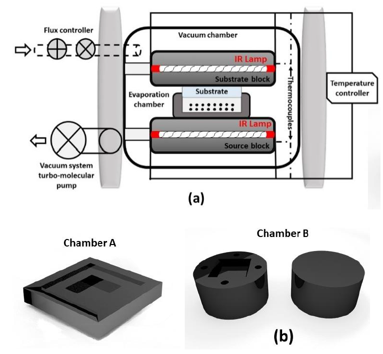
A typical superstrate structure solar cells were used to study Te region on CdTe as part of the back contact in photovoltaic devices. CdTe solar cells were fabricated using Pilkington® glass with a SnO2: F thin film around 250 nm of thickness as substrate, CdS thin layer as window material and CdTe as absorbent material. CdS films were deposited by chemical bath deposition (CBD) technique with thickness about 60 nm with an optical transmittance of 90% and a band gap value of 2.45 eV [9, 10]. CdTe absorbent material was deposited on CdS thin films by CSVT (Close Space Vapor Transport) technique under argon and oxygen atmospheres at 1mTorr to create p-n junction; Figure 1a shows the CSVT system it is consisting by two principal graphite blocks, substrate and source respectively. Between the blocks exists a graphite container A, where CdTe powder is placed and posteriorly evaporated by using source and substrate temperatures of 630 °C and 530 °C respectively for each block during the sublimation process. CdTe thickness layer about 4 µm was obtained [11]. The CdS/CdTe junction was thermally treated on CdCl2 at 450 °C by 30 min in Ar atmosphere. For simplicity the CdS/CdTe samples thermally treated on CdCl2 will be named as CdTe. A Te region was deposited on this samples by using two graphite chambers (A and B) with deposition times of 20 min and 30 min. It is well known that CdTe has a density of 5.85 g/cm3 and a melting point of 1092 °C and Te has a density of 6.24 g/cm3 and a melting point of 449.5 °C; for this reason, it is important to evaporate Te on the CdTe at temperatures no higher than its melting point. On the other hand, Te thin film on CdTe surface must be ultrathin since the Te will act as an intermediate layer between CdTe and metal junction, to improve the Ohmic properties of the semiconductor metal junction. To modify the Te growth kinetics, two types of evaporation graphite containers were designed (A and B), see Figure 1b. The A graphite container (Chamber A) is a square container with a depth of 3 mm and B container (Chamber B) is a container with small holes with a depth of 8 mm where the Te powder is placed. The CdS/CdTe junction is placed in chamber A or B; for the last case, the CdS/CdTe samples were placed inside the chamber and samples were enclosed by a graphite cap, leaving a closed chamber. The chamber A or B are placed between the source and substrate blocks allowing control rate deposition to get a nanostructured region on CdS/CdTe surface. Finally, Cu (5 nm) and Au (100 nm) metals were evaporated to conform the metal back contact.
The polycrystalline structures of the samples were measured by X-ray diffraction (XRD), X´PERT Pro MRD PANalytical X-ray system using the Cu-Kα line, morphological surface and EDS elemental analysis was made with a scanning electron microscope (SEM) JEOL series JSM7X using high accelerating voltage (5 kV). A step profiler Sloan Dektak II was employed to obtain thickness layers. Morphological measurements were performed with an Innova Veco AFM in contact mode, using a phosphorus doped Si tip. Optoelectronic behavior was studied by photoluminescence (PL) measurements at 14 K using a He-Cd (325 nm) source. To measure electrical properties a Keithley 6517B electrometer/high resistance meter was used, and electrical sheet resistance values was obtained from four-point probe measurements. How is well known, the units of ohms per square by forcing current trough two outer probes and reading the voltage across the two inner probes, this configuration avoids error due to contact resistance between probe and sample. Band gap values of CdTe and CdTe/Te were obtained by photoacoustic spectroscopy technique, a Corner Stone C130 grating monochromator coupled to Xenon lamp (1000 W) as light source were used; the light was modulated at fixed frequency using a New Focus 3502 Phase Locked Optical Chopper. An electret microphone coupled to close photoacoustic cell is used to detect the photoacoustic signal (amplitude and phase) using a Stanford Research SR850 lock-in amplifier. Photovoltaic efficiency (PV) was performed by Sol3A Class AAA Solar simulator equipment with a light source of 100 mW/cm2 (AM1.5), the electrode area is 0.08 cm2.
Results and discussion
In Table 1 the growth parameters for all samples are presented. Different Te morphologies were obtained as a function of the specific graphite container (A or B) used. CdS/CdTe junction thermally treated on CdCl2 is named as CdTe. The reported thickness corresponds to complete structure (CdS/CdTe) and Te layer. Samples were named according with the specific chamber used and deposit time. Some samples with Te layer were thermally treated in air (TT) at 400°C for 30 min.
Table 1 Growth parameter of CdTe and CdTe/Te samples
| Samples | Chamber | Source Temp. (°C) | Substrate Temp. (°C) | Deposited Time (min) | Ambient | Thickness ((m) |
|---|---|---|---|---|---|---|
| CdTe | A | 630 | 530 | 3 | CdCl2 | 4 |
| Te20A | A | 450 | 225 | 20 | - | 4.73 |
| Te20ATT | A | 450 | 225 | 20 | Air | 4.5 |
| Te30A | A | 450 | 225 | 30 | - | 5.6 |
| Te30ATT | A | 450 | 225 | 30 | Air | 4.46 |
| Te30B | B | 400 | 225 | 30 | - | 4.7 |
| Te30BTT | B | 400 | 225 | 30 | Air | 4.7 |
Figure 2 shows SEM images of CdTe thin films thermally treated with CdCl2 and Te structures covering CdTe samples. CdTe sample is formed by well-defined grains with mean sizes about 4-5 (m; small grains appear on its surface corresponding to CdCl2 grains. Te20A, Te30A and Te30B exhibit a covered surface with different morphologies, the first one corresponds to Te agglomerates, the second one shows defined grains along the sample; in both cases Te structures could be seen as a thin film. On the other hand, Te30B sample is covered by uniform Te nano structures. Te20ATT, Te30ATT and Te30BTT were thermally treated in air, this treatment modified their morphology leading grains more defined and largest. A better defined Te nanostructured layer appears covering uniformly the surface of Te30BTT sample. It is important to remark that two different Te structures were obtained one of them as a thick layer and another as nanostructured layer. These morphological properties could be important on the semiconductor/metal junction due to it could improve the electrical properties.
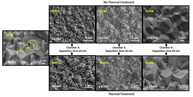
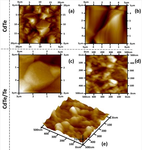
Figure 3 shows the AFM images of CdTe and CdTe covered with Te nanostructures (Te30BTT). Figures 3a and 3b show CdTe grains at different scale where well-defined grains are observed. Figure 3c shows CdTe grains covered with Te and Te nanostructure can be seen with a better definition in Figs 3d and 3e, with this nanostructure a potential barrier between CdTe and Metal is reduced increasing the efficiency of this junction.
According to the SEM results, the thermally treated samples are appropriated to continue with the analysis due to a uniform Te structure is required to be applied on photovoltaic devices. In this sense, elemental analysis (EDS) and electrical measurements, only for these samples are presented in Figure 4. Cd and Te percent content are shown in Figure 4a for each sample; the Cd and Te content for CdTe sample are 46% and 54% respectively. The deposit time affects the kinetic growth for Te layer (see Figure 2), For Te20ATT and Te30ATT, Te quantity diminish on the other hand this quantity increases for Te30BTT (see Fig, 4a). Figure 4b shows electrical properties of samples. The electrical sheet resistance values were measured from four-point probe method. Resistivity values for CdTe are reported around 105 Ω·cm [12]. All CdTe samples covered with Te showed resistivity values of 103 Ω·cm. The last results are important because the semiconductor/metal junction could be improved in electrical properties; a better Ohmic contact is probably to be obtained in this junction.
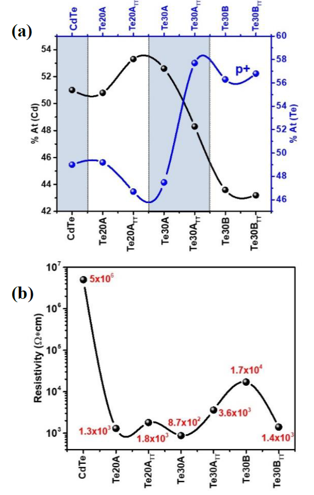
Figure 4 (a) Elemental analysis (EDS) to CdTe and CdTe covered with different Te structures and (b) Resistivity values for samples.
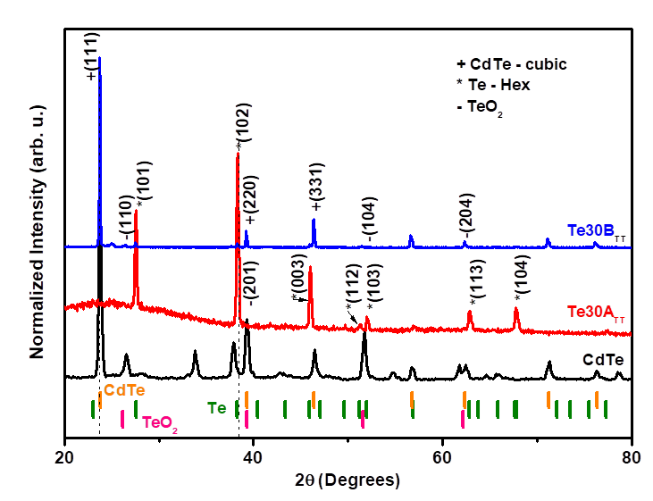
Considering the morphological and electrical properties of all samples, Te30BTT has adequate properties until now to be applied on photovoltaic devices. Figure 5 shows the X-ray diffraction (XRD) patterns of CdTe and Te30BTT; however, due to the electrical properties of the Te30ATT sample is included in the XRD spectra. Cubic-CdTe and hexagonal-Te theoretical structures are identified using PDF# 15-0770, and PDF# 36-1452 respectively. A Te crystalline structure is confirmed by XRD patterns, Te30ATT sample shows strong diffraction peaks at 27.5°, 38.8°, and 46° corresponding to (101), (102), (003) crystalline planes. For Te30BTT sample, a principal peak is located at 23.7° corresponding with (111) diffraction plane, indicating greater crystallinity.
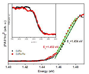
In order to determine the band gap value of all samples, photoacoustic spectroscopy (PAS) was performed. The mathematical model to describe the photoacoustic effect is determined using heat and continuity equations in which heat source is included as a result of the modulated light absorption; PAS signal is obtained as a function of photon energy, in this case the light excitation modulation fixed at 18 Hz, considering these ideas the optical absorption (α) in the equation (1) can be considered proportional to PAS signal [13, 14],
The linear extrapolation of
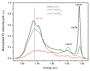
Optoelectronic properties of materials have received considerable attention due to their application in photovoltaic devices, in this sense photoluminescence (PL) measurements were made. Figure 7 shows the PL spectra of CdTe, Te30ATT and Te30BTT samples. The PL spectra show three main energy bands located at 1.59 eV, 1.55 eV and 1.44 eV. Authors have identified an excitonic emission around 1.59 eV [16, 17], the band located at 1.4 eV related to cadmium vacancy-choline complex. The range between 1.40 eV to 1.50eV is commonly associated with CdTe structure defects. Some band energy values (1.437 eV, 1.440 eV, 1.459 eV, 1.465 eV and 1.478 eV) in this range are related to CdSxTe1-x intermixing [18], VCd-ClTe transition, donor-acceptor pair (DAP) transition, VCd-ClTe transition and Y-band (phonon replicas) [19] respectively. The 1.55 eV emission is related with oxygen, the incorporation of this oxygen, it could be located in a Te site as an isoelectronic defect or TeO2 formation. On the other hand, TeO2 phase is corroborated by XRD difractograms (See Figure 5).
Te structures performance on CdTe solar cells
CdTe solar cells were developed by using CdS (60 nm) and CdTe (4 (m) as window and absorbent layers; CdS/CdTe junction was thermally annealed on CdCl2 and after thermally treated in air. Different Te morphologies on CdS/CdTe junctions were deposited; Cu/Au was used as metal back contacts with an area of 0.08 cm2. Cu is commonly used as back contact due to its efficient electrical properties; different Te layers were deposited on CdTe surface to reduce the Cu diffusion along the photovoltaic solar cell improving the semiconductor/metal junction. All solar cells (SC) configurations are represented in Figure 8a, each one has a specific Te layer under study SC1:Te20A, SC2:Te20ATT, SC3:Te30A; SC4:Te30ATT and SC5:Te30BTT. Traditional configuration of CdS/CdTe photovoltaic device without Te layer was named CdTe. All solar cells were evaluated considering an illuminated area of 0.08 cm2 under global AM 1.5 solar spectra, In Table 2 are showed the best result of each solar cell. No antireflection coatings were used.
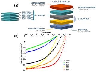
Figure 8 (a) Schematic CdTe and CdTe/Te devices and (b) J-V measurements for all photovoltaic devices
Table 2 Electrical parameters of CdTe and CdTe/Te photovoltaic devices.
| Devices | VOC (mV) ± 1 mV | JSC (mA/cm2) ± 3mA/cm2 | FF (%) ± 0.6% | n | η (%) ± 0.8% |
|---|---|---|---|---|---|
| CdTe | 638 | 24 | 43 | 13 | 6.8 |
| SC1 | 560 | 12 | 30 | 14 | 1.4 |
| SC2 | 560 | 14 | 36 | 12.2 | 2 |
| SC3 | 620 | 27 | 51 | 8.6 | 6.1 |
| SC4 | 720 | 28 | 51 | 6.9 | 7.5 |
| SC5 | 730 | 28 | 60 | 5 | 12 |
Figure 8b shows the J-V electrical behavior for all devices, electrical parameters as short current density (JSC), open circuit voltage (VOC), fill factor (FF) values and photovoltaic efficiency (η) are shown in Table 2. These characteristics were influenced by the specific photovoltaic structure and Te morphology. Te layer used as part of the back contact improves the JSC, VOC and FF values. Inadequate ideality factor and the photovoltaic efficiency values were obtained when Te as layer is used as part of the back contact in CdTe photovoltaic devices. On the other hand, nanostructured Te on CdS/CdTe junction improves the VOC and FF values due to nanostructures Te helps to create a good depletion region between CdS/CdTe junction, and it reduces the recombination mechanism. The photovoltaic efficiency was improved by nanostructure Te used as part of the back contact in CdTe solar cells. Te thicknesses greater than 1 µm increase the potential barrier so, the photo generated electrons energy is not enough to cross this potential barrier.
The ideality factor diode (n) was determined by Cheung method for each solar cell. Considering this method, the relationship between some electrical parameters at temperature T involving the one diode model is given by:
Equation (2) enables the calculation of ideally factor diode n, where k is the Boltzmann constant, applied voltage (V), shunt and series resistance (R s , R sh ), and I lig is light current, when solar cell is under illumination [20].
Series (R s ) and shunt (R sh ) resistance values for all photovoltaic devices are presented in Figure 9. Te thickness
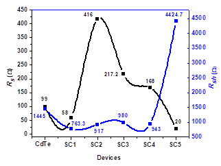
modified the series resistance, also in this sense nanostructure Te layer decreases the R s values in photovoltaic devices. Nanostructured Te used in CdTe/metal junction reduces the R S values and thermal treatment in this case improves this value. On the other hand, R sh values increases when nanostructured Te with a thermal process is employed as part of the back contact.
Conclusions
CdTe photovoltaic solar cells were fabricated, considering Te as a film and as a nanostructure as part of the back contact. Chamber A and B were designed to modified Te growth on CdTe surface, in this way, p+ Te region was obtained as thick layer and nanostructured Te region respectively. This part is important because it is necessary to create a p+ Te intermediate layer to improve the electrical properties between CdTe/metal junction.
A Te uniform region was obtained by using Chamber B, in this case CdTe grains were covered by the Te as nanostructured region allowing to reduce grain boundaries it means potential barriers reduction leading an easily carries mobility to the back contact. Electrical parameters of CdTe solar cells were improved by using nanostructured Te region as buffer layer, the FF and VOC values varied from 30% to 60% and 560 mV to 730mV respectively. The electrical resisitivity in CdTe was reduced from 106 Ω·cm to 103 Ω·cm, series and shunt resistance were reduced and increased due to nanostructured Te as buffer layer. A Te thick layer was obtained on CdTe by using Chamber A, in this case the FF and VOC values were decreased thus decreasing the photovoltaic efficiency. Therefore, to improve the electrical properties of the semiconductor/metal junction, it is better to use a nanostructured Te region than a film of Te.

