


 text new page (beta)
 English (pdf)
 Article in xml format
 Article references
 Send this article by e-mail
 Cited by SciELO
  Similars in
SciELO
Similars in
SciELO 
 Permalink
Introduction
Organic thin film transistors (OTFTs) have attracted interest for large area electronic applications due to the compatibility with low cost and low temperature fabrication processes. Depending on the device configuration, several parasitic effects could limit its performance. Among the most important effects, parasitic series resistance has been reported to strongly affect the electrical performance of the thin film transistors (TFTs) [1]. In fact, as the resistance of the channel decreases, the contact resistance becomes increasingly important, in particular in short channel devices. Series resistance can be influenced by metal contact, film thickness, device architecture, substrate roughness, device processing, and temperature [2-6]. Therefore it is important to analyze the two typical contact configurations used for OTFTs: top-contact (TC) and bottom-contact (BC). For example, the deposition of the active layer in BC-TFTs is the last fabrication step; therefore the semiconductor is not exposed to other processes as in TC-TFTs. However, BC-TFTs have showed several drawbacks compared to TC-TFTs, as the application of a gate voltage induces a channel with a higher conductivity at the semiconductor/dielectric interface [7]. TC-TFTs have exhibited contact resistance (Rc) of about one order of magnitude higher than BC-TFTs [8] and Rc dependence on the pentacene/Au thickness ratio [9].
Another important effect limiting the OTFT performance is the degradation of the active layer when exposed to ambient, as a result of oxygen diffusion in the bulk of the material. The oxygen absorption in the active layer degrades the current-voltage characteristics [10]. For pentacene OTFTs, researchers have found still functional devices with decreased performance in terms of field-effect mobility (μ), on-current, I on/off ratio and threshold voltage (V T ) shifting even after degradation [11-12].
Although researchers have analyzed the influence of the pentacene degradation in the performance of the OTFTs, they only focus in the main parameters such as μ and drain current (I d ) [13-14]. In this reports, it has been neglected other important parameters of equally importance; for example, the parasitic resistance. In general, different authors in different reports have described the characteristics of pentacene-based OTFTs in terms of active layer thickness [8,15,16], devices structure [1-2,7,16] and degradation [10-14]. However, a complete analysis for the same OTFT technology has not been reported.
In this study, the influences of three combined effects on the Rc: a) active layer thickness, b) device architecture and c) semiconductor degradation are investigated in pentacene-based OTFTs. This analysis can be applied to other organic dielectric/semiconductor systems. We fabricated TC and BC TFT configurations with a SiO2/parylene dielectric bilayer to minimize the leakage current. The stability and lifetime of the TFTs were analyzed.
Experimental details
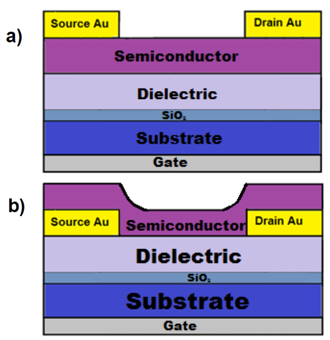
OTFTs were fabricated using a highly doped p-type silicon wafer with a back common aluminum layer used as gate electrode. First, 190 nm of parylene-C were deposited by chemical vapor deposition on top of 50 nm of thermally grown SiO2 to form a gate dielectric bilayer. SiO2 helps to reduce the gate leakage current, whereas parylene-C improves the dielectric/semiconductor interface with pentacene [17,18]. Next, aluminum gate metal was deposited on the backside of the wafer. Then, three pentacene film thicknesses 50 nm, 100 nm and 150 nm were sublimated while the substrate was kept at room temperature. In order to define BC and TC configuration the 150 nm thickness contacts were deposited, using a shadow mask, by e-beam evaporation prior to, or after, the pentacene deposition, respectively. BC-TFTs and TC-TFTs are shown in Figure 1a) and 1b), respectively.
OTFTs were electrically characterized immediately after fabrication using a Keithley 4200 semiconductor characterization system. OTFTs were also measured one and two months after being stored at room temperature in dark ambient conditions.
Results and discussion
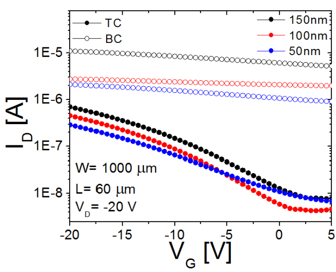
Figure 2 shows the transfer characteristics of BC-TFTs and TC-TFTs fabricated with three different pentacene thicknesses. As can be seen, I D is higher for BC-TFTs (open symbols) and the devices remained always on, which is the result of a less resistive path for the current between source and drain compared to TC-TFTs (solid symbols) configuration. In BC-TFTs, the holes are injected/collected directly from the sidewall of the electrodes to the channel. Therefore, the current flows parallel to the polymer chains and the overall resistance the carriers experience in BC-TFTs is lower than in TC-TFTs, where the carriers need to flow vertically from the contact through the pentacene bulk in order to reach the channel, resulting in an additional resistance component that limits the electrical current.
V t and μ for TFTs were calculated from the extrapolation and slope of the √I D vs. V g curve measured in saturation respectively, following the expression for I D in MOS transistors:
where C ox is the dielectric capacitance per unit area; W is the channel width and L is the channel length.
Calculated V T for BC-TFTs is more positive compared to TC-TFTs, due to the higher channel and bulk conductivity resulting from the higher carrier injection and the direct contact between the accumulation layer and the source-drain (S-D) contacts that does not allow to completely close the channel [19]. Carrier injection from S-D electrodes in BC-TFTs is expected to be higher; however, with a smaller effective contact area compared to TC-TFTs. This VT increment in BC-TFTs is due to overestimations for short channel devices using the square-root-of-current-extrapolation (SRE) method [20], which is greatly affected by series resistances [21].
TC-TFTs presented mobilities one order of magnitude higher (4.8 × 10⁻² cm2/Vs) than BC-TFTs (1 × 10⁻³ cm2/Vs). Changes in mobility on BC-TFTs have been attributed to contact (semiconductor/metal) effects due to a dipole barrier that can shift the vacuum level upward by more than 1 eV, avoiding carriers to reach the HOMO level [22-24]. However, mobility is not dependent on the contacts used in the TFT and is normally dictated by the dielectric/semiconductor interface in both TC and BC structures. Therefore, the differences in the calculated values for mobilities between the two structures could be misleading and the result of the use of a TFT model that does not include a term related to the contact effects and bulk current. Also, we observed for all the pentacene thicknesses a channel length dependence in BC-TFTs, as μ increased almost an order of magnitude for larger channel lengths, whereas for TC-TFTs μ remained almost constant for all the channel lengths. Since the contact effects are not considered in the model, it can be assumed that more accurate values are obtained for larger channels (80 μm) where the contact resistance effects are less important (Table 1).
Table 1 Behavior of μ for devices with L = 80 μm.
| Thickness | μ (cm2/V-s) | |
|---|---|---|
| (nm) | TC | BC |
| 50 | 8.7 × 10⁻³ | 4.41 × 10⁻³ |
| 100 | 1.4 × 10⁻² | 5.41 × 10⁻³ |
| 150 | 4.8 × 10⁻² | 8.59 × 10⁻³ |
Contact Resistance
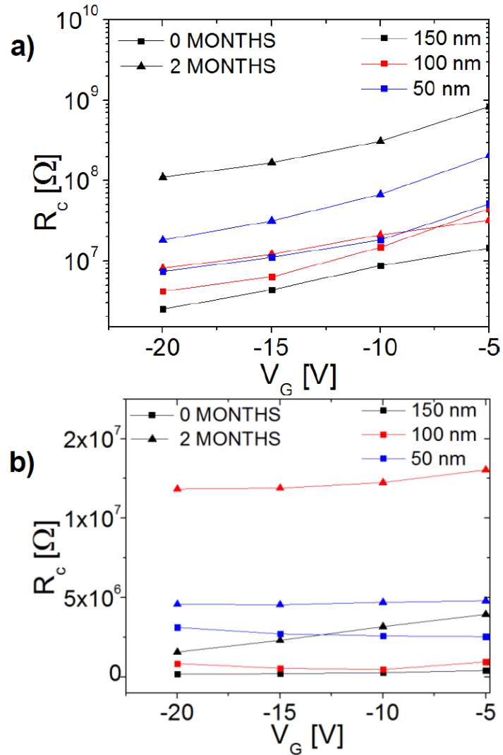
Rc was obtained from experimental data at V d = 3.5- V in the linear regime using the transmission line method (R vs. L) [25]. TC-TFTs presented a higher contact resistance (107 Ω) than BC-TFTs (105 Ω). Rc seems to be reduced as VG is increased for TC-TFTs, whereas for BC-TFTs, Rc remained in the same order of magnitude for all the pentacene thicknesses, see Figure 3. Higher contact resistance in TC-TFTs could be due to an additional resistance presented in the structure from the vertical transport through the bulk of pentacene that limits carrier injection from the semiconductor/contact interface to the channel.
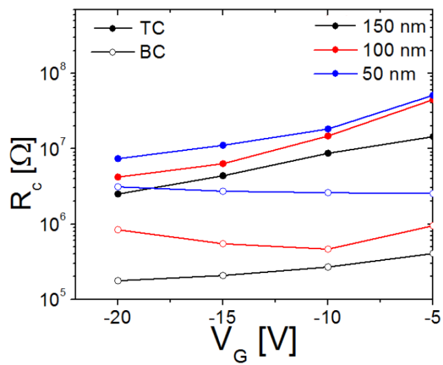
When V g becomes higher, the barrier the carriers see is reduced and the conduction is no longer limited by the bulk, reducing Rc. In BC-TFTs this barrier is very small and there is no V g dependence [25]. Nevertheless, both configurations presented the same trend of contact resistance in terms of semiconductor thickness, where the thinnest TFTs presented the highest contact resistance. This effect can be related to thickness ratio between the S-D contacts and the semiconductor. Thinner semiconductor films do not cover entirely the height of the contacts in case of the BC-TFTs, therefore the contacted area is smaller compared to thicker semiconductor films. In case of the TC-TFTs, the increase of the contact resistance with decrease in film thickness may be due roughness and grain size of the polycrystalline semiconductor. Results reported in [26] indicate that grain size increases with increasing thickness of polycrystalline films. In [27,28] was shown an increase in the mobility with increasing grain size and decreasing surface roughness. And, a decrease of the contact resistance was observed in [29] due to an increase in field-effect mobility of pentacene TFTs.
Degradation
Figure 4 shows the transfer curves for TC-TFTs with 150 nm pentacene films (devices with higher mobility) after one and two months of being fabricated. Degradation produced a decrease in μ and a shift in the V T . Mobility decreased almost an order of magnitude per month in both configurations. V t on TC-TFTs tends to increase and the maximum on-current is reduced by an order of magnitude per month, as shown in Table 2, nevertheless I on/off ratio remains in the same order of magnitude after 2 months. Similar results have been reported in [30,31], where a drop in field-effect mobility, threshold voltage and drain current was obtained as a result of active layer degradation after 1320 h the pentacene TFTs were fabricated.
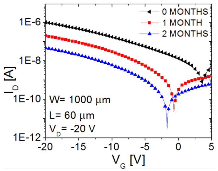
Table 2 Behavior of μ, I D , Ion/off ratio and V T considering two months analysis.
| Month | μ (cm2/V-s) | Vt (V) | i Dmax (A) | I on/off ratio (A) | ||||
|---|---|---|---|---|---|---|---|---|
| TC | BC | TC | BC | TC | BC | TC | BC | |
| 0 | 3 × 10⁻² | 1.7 ×10⁻² | 3.1- | 64.56 | 1.01 × 10⁻⁶ | 2.26 × 10⁻⁶ | 9.83 × 101 | 12.7 × 10⁻¹ |
| 1 | 8 × 10⁻³ | 3 × 10⁻³ | 3.3- | 27.04 | 2.04 × 19-7 | 7.8 × 10⁻⁷ | 8.23 × 101 | 17.9 × 10⁻¹ |
| 2 | 2 × 10⁻³ | 4 × 10⁻⁴ | 4.96- | 16.87 | 4.79 × 10⁻⁸ | 1.1 × 10⁻⁶ | 6.29 × 101 | 15.9 × 10⁻¹ |
Figure 5 shows contact resistance for both configurations. In both cases, contact resistance becomes higher after two months, which indicates also degradation at the semiconductor/metal interface that follows the same trend in terms of V g for each TFT configuration.
This behavior might be due to OH and C-H2 defects in pentacene after the material has been exposed to oxygen and humid environments. These defects modify the structure of the pentacene molecule and produce localized states in the bandgap as well as hole trapping at the grain boundaries, where C-H2 defects form a C22H15 molecule and one of the C atoms becomes fourfold coordinated. On the other hand, OH forms a C22H13O molecule in which there is a C-O double bond by replacing one of the hydrogen atoms by an oxygen atom [32].
Considering also that the morphology of polycrystalline pentacene films is relatively open, with large crevices between the grains that run almost all the way down to the first few monolayers on the substrate [33] and that pentacene is highly hydrophobic, H2O molecules can easily diffuse into crevices modifying the morphology of the film, inducing a phase transition from a thin film phase to a bulk- like phase [34]. Also, interacting with the trapped carriers at the grain boundaries by limiting the charge transport and therefore, affecting the performance of the devices [35].
Rc increases with time and conductivity through the channel is reduced by the limited carrier transport. Oxygen located in the bulk of the film can continue absorbing oxygen from ambient, as it has been found this for the same semiconductor/contact thickness and for thinner pentacene films. In the thickest TC-TFTs, Rc increases more over time because it is more likely to have more defects and traps with increasing grain size. In the case of the BC-TFTs with 100 nm pentacene films Rc increases more rapidly maybe due to humidity does not reach the dielectric/semiconductor interface and pentacene films continue absorbing oxygen from the ambient, also defects may be lower, not affecting as much as the TC-TFTs performance.
Conclusions
In summary, an analysis due to the effects of the active layer thickness, device architecture and pentacene degradation on the Rc of the OTFTs was presented. Devices presented thickness dependence; this may be due roughness and grain size of the active layer. Devices with thicker active layer presented a better performance, TC-TFTs presented higher mobility as high as 4.8 × 10⁻² cm2/Vs compared to BC-TFTs (4.41 × 10⁻³ cm2/Vs). Also, the results were less sensitive to geometry of the device (channel length). In terms of configuration, TC-TFTs show a more resistive channel (107 Ω) and a V g dependence compared to BC-TFTs for almost an order of magnitude (105 Ω). This effect might be due to BC-TFTs have a smaller Au-contact area and therefore a smaller carrier injection at the contact/semiconductor interface. We have to consider that BC-TFTs have a metal-insulator-metal structure, where S-D contacts are directly in contact to the channel and dielectric layer is exposed to contact deposition process, whereas TC- TFTs have a metal-insulator-semiconductor structure where the active layer is exposed to the contact deposition process. Despite oxygen and moisture from the environment contributes to the active layer degradation, which affects to the performance of the device, OTFTs still be functional after 2 months, nevertheless with a decrease of an order of magnitude in terms of μ (10-2 - 10-3 cm2/Vs) and I Dmax (1 × 10⁻⁶ - 4.79 × 10⁻⁸ A), while Rc increase two orders of magnitude (2.49 × 10⁶ - 1.1 × 10⁸ Ω) for TC-TFTs and an order of magnitude (1.76 × 10⁵ - 1.57 × 10⁶ Ω) for BC-TFTs, due to hole trapping and oxygen absorption in the active layer.

