


 text new page (beta)
 English (pdf)
 Article in xml format
 Article references
 Send this article by e-mail
 Cited by SciELO
  Similars in
SciELO
Similars in
SciELO 
 Permalink
Introduction
The chemical bath deposition (CBD) method is a simple and inexpensive technique that has been widely applied to the fabrication of semiconductor layers for photovoltaic applications [1]. CdS is an n-type semiconductor material with a band gap of about 2.42 eV that can be easily deposited by CBD [2]. CdS has been used in various applications like optoelectronic devices (solar cells) [2-5], TFT transistors and CMOS circuits, among others [6-9]. It has been reported that different S/Cd ratios during reactions can modify the characteristics of CdS film [10]. The electrical resistivity of CdS can be controlled by applying different annealing treatments or by varying the deposition time, atmosphere and thiourea concentration during the CBD process [11]. Other studies have shown that the electrical characteristics of CdS can be changed by doping with Mn, Cu, Ni, Co, Ga, B, Ag, etc. [12-19]. In some studies, CdS was even converted into a p-type semiconductor [20]. In this research, CdS thin films were synthesized by chemical bath deposition and behaved as an n-type semiconductor. The CdS films were doped with copper through diffusion of 80-nm-thick copper films into the films under annealing treatments. Several properties of the films were studied, including crystalline structure, chemical composition, morphology and optical properties.
Experimental details
CdS thin films were deposited on Corning 7051 glass substrates by using two different precursor solutions with the following formulations:
A. 50 ml of deionized water, 4 ml of 0.1 M cadmium nitrate tetrahydrate (Cd(NO3)2 4H2O), 20 ml of 0.5 M ammonium chloride (NH4Cl), 5 ml of 0.3 M potassium hydroxide (KOH), 5 ml of buffer, pH 11 [NH4OH/NH4Cl] and 10 ml of 0.5 M thiourea SC(NH2)2; and
B. 50 ml of deionized water, 4 ml of 0.1 M cadmium nitrate tetrahydrate (Cd(NO3)2 4H2O), 20 ml of 0.5 M sodium citrate (Na3C6H5O7), 5 ml of 0.3 M potassium hydroxide (KOH), 5 ml of buffer, pH 11 [NH4OH/NH4Cl] and 10 ml of 0.5 M thiourea SC(NH2)2.
The mixtures were placed at 77.7 °C in a thermal water bath without stirring. Substrates were vertically immersed in the solution and removed after 55 or 90 minutes, to get A-55, A-90, B-55 and B-90 CdS samples where A and B indicate precursor solution and 55, 90 indicate deposition time.
The samples were of a homogeneous yellowish color, were specularly reflecting and had very good adhesion to the substrate. The thickness of the films was measured using a KLA-Tencor P-15 surface profiler. The films had an average thickness of 130 nm (Figure 1). The B-90 film was selected to be doped with copper due to the best optical and morphological properties. Using an evaporation method, a metallic copper layer of about 80 nm thickness was deposited over the B-90 film (Figure 1), which were then subjected to different annealing temperatures (Ta) equal to 140, 170, 200 and 230 °C for 20 minutes, in order to allow copper diffusion into the films. The conditions to get the Cu film evaporated on the CdS layer was not so finely controlled, substrate temperature is room temperature, and the source metal is copper vacuum gasket bites; after to arrive the tungsten resistance-filament to 30 Amps, the ceramic crucible start to evaporate the copper bites, coating the CdS layer and the window chamber in around 4 minutes; when start the vacuum thermal deposition, the pressure is around 1×10⁻⁴ Torr. Being a thickness of 80 nm. The CdS:Cu samples were labeled as: B-90-140, B-90-170, B-90-200 and B-90-230 for Ta = 140, 170, 200 and 230 °C, respectively. The copper-covered B-90 film that was not thermally annealed was labeled as B-90-Troom. A JEOL JSM-7600 field-emission scanning electron microscope (SEM) equipped with a beryllium window X-ray detector was used to obtain morphology and chemical composition of the samples. This equipment has two secondary electron detectors: an upper detector (SEI) and a lower detector (LEI) also it has a backscattered electron detector that can collect electrons at low takeoff angle (LABE) which are extremely sensitive to subtle changes in localized topography of the sample surface and give information on compositional differences or on the inner structure of samples. A JEOL 2010F TEM field-emission transmision electron microscope (TEM) was used to obtain morphology and crystalline structure of de samples. Chemical composition analysis was performed by energy dispersive spectroscopy (EDS). Roughness of the surface films was measured by atomic force microscopy (AFM) with an AFM system (Nanoscope III). Crystalline structure was analyzed by X-ray diffraction (XRD) using a Rigaku Ultima IV X-Ray diffractometer with Cu kɑ radiation (40 kV/44 mA, 0.5 °/min, 10 ≤ 2θ ≤ 50, λ = 0.15418 nm) at normal incident. Identification of the hexagonal phase and indexing of the peaks in the XRD patterns were carried out using JCPDS card #41-1049 for cadmium sulphide, JCPDS card #35-1091 for copper oxide, JCPDS card #653288 for cubic Cu2O, and JCPDS card #04-0836 for copper.
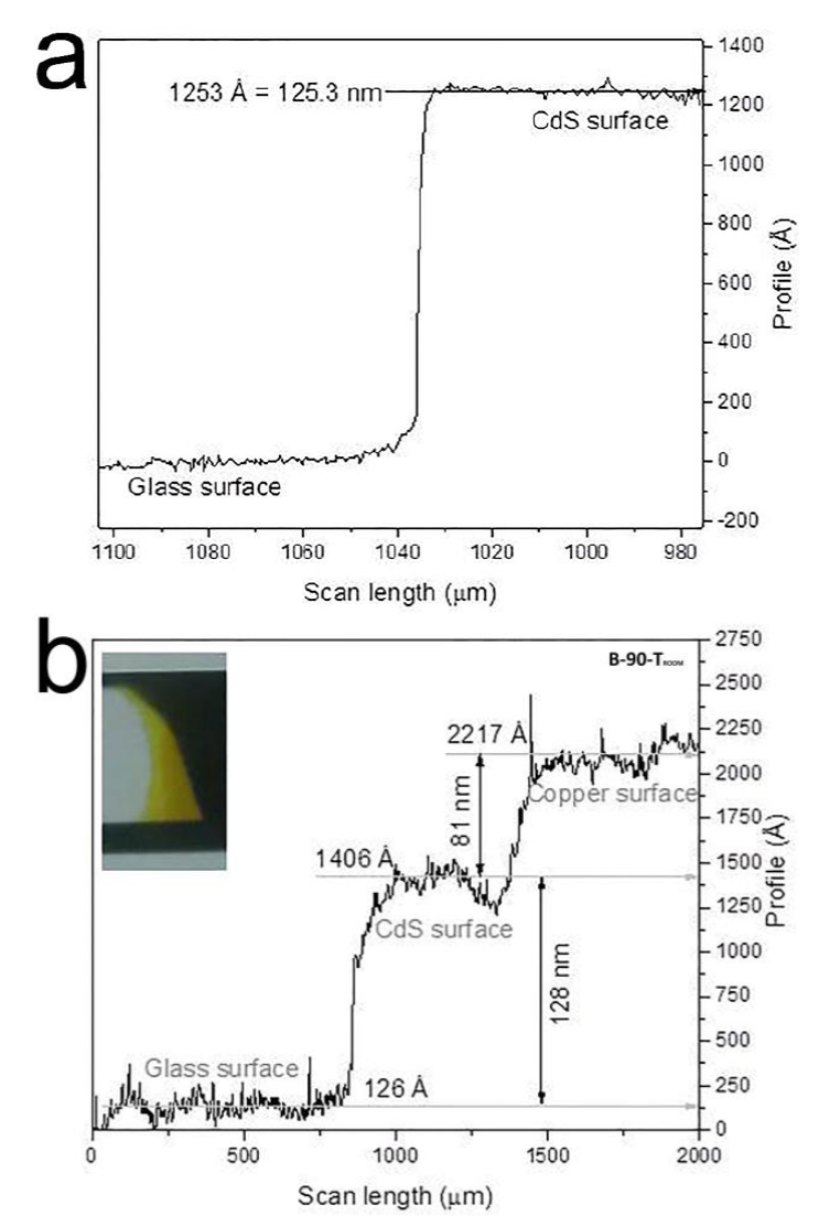
Figure 1 Surface profilometry measurement of: a) B-90 and b) B-90-Troom films, deposited by CBD and CBD followed by evaporation, respectively.
Photoluminescence (PL) excitation and emission spectra at room temperature (Troom) were recorded using a spectrofluorometer SPEX Fluoro-Max-P Lamp intensity correction is performed automatically by this instrument: it measures excitation light intensity with an additional photomultiplier tube and performs the correction accordingly before displaying the data. The absorption spectra of the films were measured by Cary 5000 spectrophotometer (Varian and Avantes AvaSpec-2048-USB) in the range from 350 nm to 800 nm. Resistivity was measured using an Ecopia HMS-3000 Hall Measurement System which provides precision measurements with percentual uncertainty less than 5 %.
Results and discussion
Morphology
Figure 2 shows changes in the morphology of the CdS films obtained from the formulation with ammonium chloride as a complexing agent and deposition times of 55 and 90 minutes. Both A-55 and A-90 films were composed of submicron spherical-shaped particles with few particles bigger than the average size. Average particle size was higher for A-90, indicating that a higher deposition time produces bigger particles. The A-55 and A-90 films had discontinuous surfaces with free spaces of about 600 nm and 400 nm, average particle sizes of 71.3 nm and 112 nm, and particle-size distribution functions with Full Width at Half Maximu (FWHM) of 0.50291 nm and 0.37171 nm, respectively. Both films showed nodular growth. It is worth noting that higher deposition times allowed the coalescence of nanoparticles, hence minimizing the number of free spaces and, apparently, film roughness (see Figures 2 c and 2d).
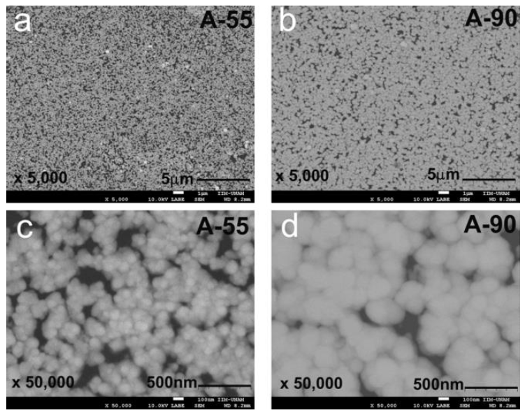
Figure 3 shows changes in the morphology of CdS films obtained from the formulation with sodium citrate as a complexing agent and deposition times of 55 and 90 minutes. Both B-55 and B-90 films had continuous surfaces, without cracks, made of splinter-shaped nanoparticles. The films showed a few submicron particles resulting from the coalescence of nanoparticles, achieving sizes of 500 nm for the B-90 film and 400 nm for the B-55 film (see Figures 3a and 3b). This translated into surfaces with heterogeneous morphology.
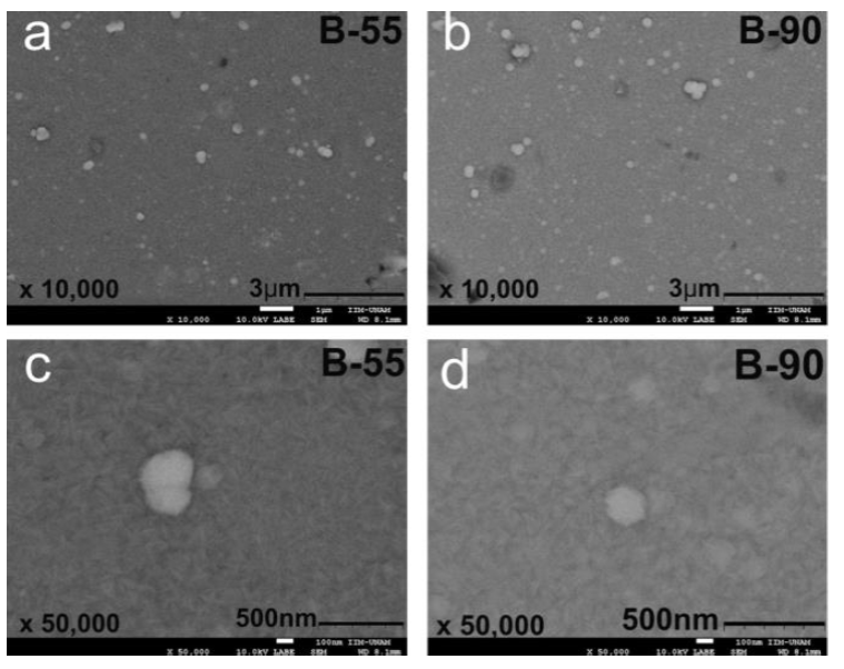
The micrographs of both films showed only a few black spots indicating zones with different chemical compositions. This suggests that films had a nearly homogeneous chemical composition.
B-55 and B-90 films showed splinter-shaped particles with width distribution functions centered at 31.7 nm and 37.5 nm, and FWHM of 0.603 nm and 0.5198 nm, respectively. At first, film roughness appeared to be in the nanometric range, like the width of the splinters. The average size of splinters increased with deposition time, indicating that a higher deposition time produces bigger splinters.
From the above, it appears that the B-90 film resulted in a better morphology for potential solar cell applications.
Figure 4 shows a SEM micrograph in LABE mode of the copper film deposited on the B-90-Troom sample, in order to examine its morphology for the purpose of copper doping. The film turned out to be continuous and without cracks, with a few particles of submicron dimensions (~500 nm). There are three things worth mentioning about the copper film: 1) The film appeared to have a uniform chemical composition across its surface; 2) The film's surface was composed of spherical-shaped nanoparticles; and 3) At first glance, film roughness appeared to be in the nanometric range.
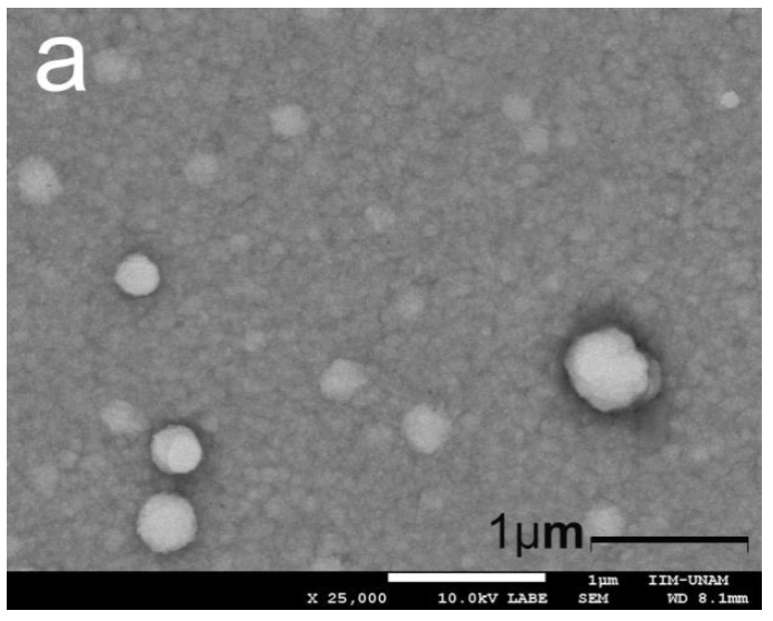
Figure 5 shows the morphology of the B-90-Ta film as a function of Ta. Figures 5 a, 5c, 5e and 5g show micrographs of B-90-Ta samples for Ta = 140, 170, 200 and 230 °C, respectively. The micrographs reveal a surface composed of spherical-shaped particles and the presence of relatively big particles and potholes. The films annealed at 140 and 170 °C turned out to be morphologically similar (Figure 5d) but had different average particle size: 160 nm and 38 nm, respectively.
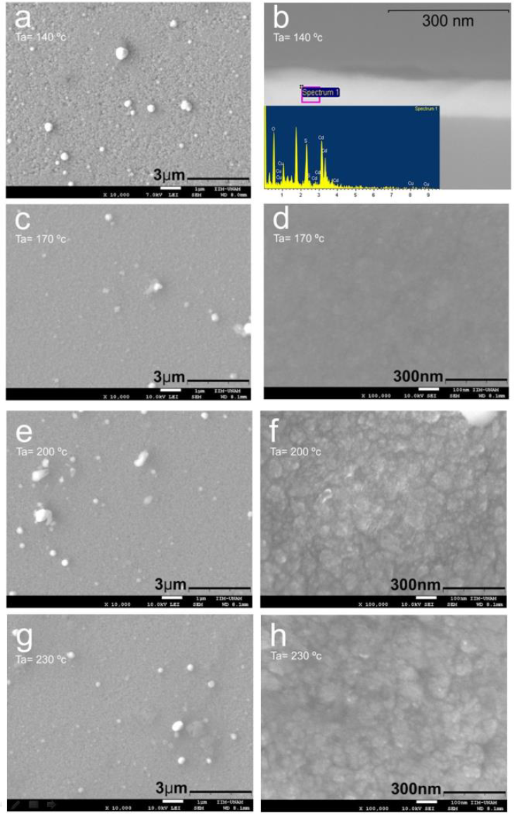
Figure 5 SEM micrographs of the samples B-90-Ta for Ta = 140, 170, 200 and 230 °C. Figure 5b shows the backscattered electron image of the cross section of the sample B-90-140.
For Ta of 200 °C and higher, however, there was a change in morphology, with film surfaces composed of nanoclusters of spherical-shaped nanoparticles of 10 nm diameter, as shown in Figures 5 f and 5h. The average size of the clusters was of 65 nm and 56 nm for Ta = 200 and 230 °C, respectively. At first glance, film roughness appeared to be in the nanometric range. It is evident from the lower secondary electron images in Figures 5a, 5c, 5e and 5g that the films had a homogeneous chemical composition across their surface for all Ta values.
Figure 5b shows a micrograph of a cross section of the B-90-140 sample obtained by using low-angle backscattered electrons (LABE). A bilayer film of about 160 nm is observed, a result representative of all synthesized samples.
The upper film was 15 nm thick on average, but was thicker in certain zones. The inset in figure 5b shows an EDS analysis of the zone evidencing that Cu ions were incorporated into the film.
Crystalline structure
The crystalline structure of the A-55, A-90, B-55 and B-90 samples was obtained by XRD. Figure 6 shows that the crystalline phase of CdS films was cubic and did not vary with deposition time or the formulation, which is consistent with the results of Atefeh Jafari et al. [21]. The XRD pattern showed a wide band and three main peaks c entered at 2θ = 24.89 °, 26.51 ° and 43.99 °. The wide band was attributed to amorphous material. The peak centered at 2θ = 24.89 °, particularly the highest diffraction peak (111), was attributed to the presence of monoclinic CdSO4-H2O [22].
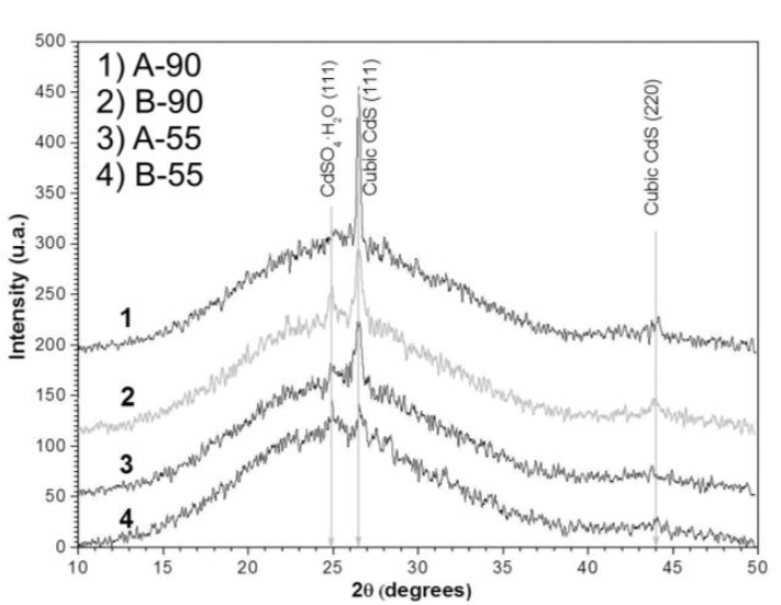
Indeed, this peak disappeared after thermal annealing, used to diffuse copper into the CdS film (see Figure 8). The peaks centered at 2θ = 26.51 ° and 43.99 ° were attributed to the (111) and (110) planes of the cubic crystalline phase of CdS. All samples had a lattice constant of 5.8196 Å and a preferred growth orientation along the (111) plane.
The crystalline grain sizes were obtained by Debye-Scherrer formula [23]:
Where: D = crystalline grain size, λ = CuKɑ radiation at 1.5426 Å, β = Full Width at Half Maximum of diffraction peak and θ = half of 2θ diffraction angle . The calculated D values were: 31.4 nm, 20.4 nm, 19.4 nm and 14.5 nm for the A-90, B-90, A-55 and B-55 films, respectively. This provides evidence of the greater effectiveness of sodium citrate (Formulation 3) than ammonium chloride (Formulation 2) as a complexing agent.
In Figure 7, the B-90 sample showed a film containing regularly spaced, asterisk-shaped black entities. These asterisks had a narrow size distribution function centered at 30 - 40 nm and were composed of several superposed nanocrystals smaller than 10 nm (Figure 7d). This is consistent with the average grain size obtained by XRD. These nanocrystals showed crystalline planes located far away from each other at 3.33 Å, corresponding to the (111) planes of cubic CdS (Inset in figure 7d). The electron diffraction pattern of the film (Inset in figure 7e) showed crystalline planes corresponding to the (111) planes of cubic CdS, with d(111) = 3.35 Å. This resulted in a lattice constant of 5.8024 Å, which is consistent with the lattice constant of 5.8196 Å obtained by XRD.
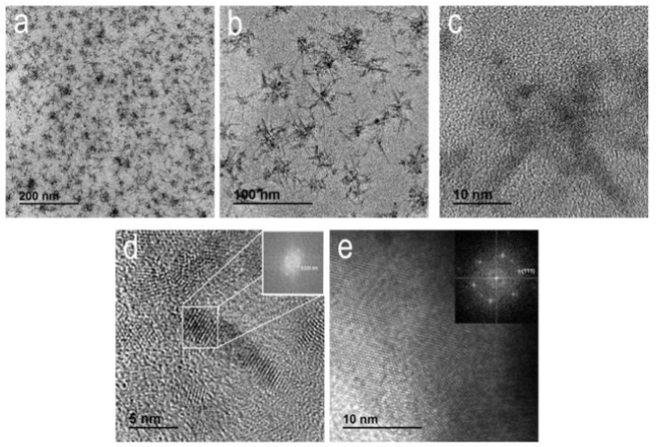
Figure 8 shows the XRD pattern of the B-90-Ta samples as a function of Ta, as well as the diffraction pattern of the B-90-Troom sample, that is, the sample that had a copper film deposited on its surface, but was not heat treated. The first sample showed peaks centered at 27.3 ° and 44.61 °, as well as a wideband. The peaks were attributed to the (111) and (220) planes of cubic CdS, and the wideband, to material that was still crystallizing and/or the amorphous copper film deposited by thermal evaporation [24].
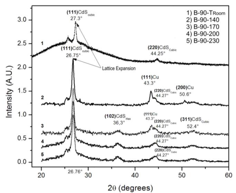
Figure 8 X-ray diffraction patterns as a function of Ta of the B-90-Ta samples and of the B-90-Troom sample.
After thermal annealing, the XRD pattern presented peaks at 26.76 °, 36.3 °, 43.3 °, 44.25 °, 50.6 ° and 52.4 °. The peaks centered at 26.76 °, 44.25 ° and 52.4 ° were attributed to the (111), (220) and (311) planes of cubic CdS [21]. The peaks centered at 43.3 ° and 50.6 ° belonged to cubic copper [25]. The peak centered at 36.3 ° as well as the low-intensity peaks in the region of 25 - 26 ° were attributed to traces of hexagonal CdS, in agreement with Kashiwaba et al. [26].
Although it might be thought that the 36.3 ° peak could correspond to the (111) planes of cubic Cu2O [25], this could not be the case here because Cu2O is formed simply by exposing copper to the oxygen in the air, and this 36.3 ° peak was not observed in the diffraction pattern of the B-90-Troom sample, which had a copper film exposed to the air for a long time. The average grain size for cubic CdS, hexagonal CdS and cubic Cu was 16 nm, 8 nm and 13 nm, respectively. The sample that was thermally annealed at Ta = 140 °C was the only one not showing CdS in its hexagonal phase.
All thin films showed CdS mainly in its cubic crystalline phase and a preferential growth along the (111) planes. Figure 8 shows a shift of cubic peaks towards lower 2θ values, indicating a uniform expansion of the CdS lattice as copper replaced Cd. There are two things worth mentioning in the XRD pattern of the B-90-Ta films as a function of Ta: the presence of cubic copper at Ta = 140 °C, which disappears as Ta increases; and the presence of hexagonal CdS, starting at Ta = 170 °C and becoming more evident as Ta increases.
Electrical properties
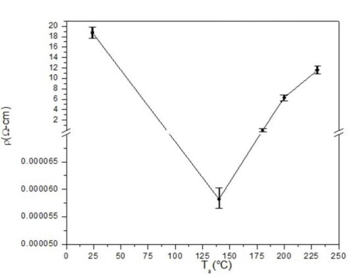
Figure 9 shows the resistivity of copper-doped CdS film as a function of Ta. It can be observed that resistivity decreased drastically as Ta decreased, which seemed to be associated with a higher amount of crystalline copper and/or the predominance of cubic CdS over hexagonal CdS, in accordance with the results shown in the section Crystalline structure above. Further studies are required, however, to clarify the relationship among the above factors, and this is foreseen as future work. The lowest resistivity obtained was 5.822 χ 10-5 Ω-cm for the B-90-140 sample, which showed the highest amount of cubic copper and no hexagonal CdS.
Optical properties
The absorbance spectra of the A-90, A-55, B-90 and B-55 samples are shown in Figure 10.
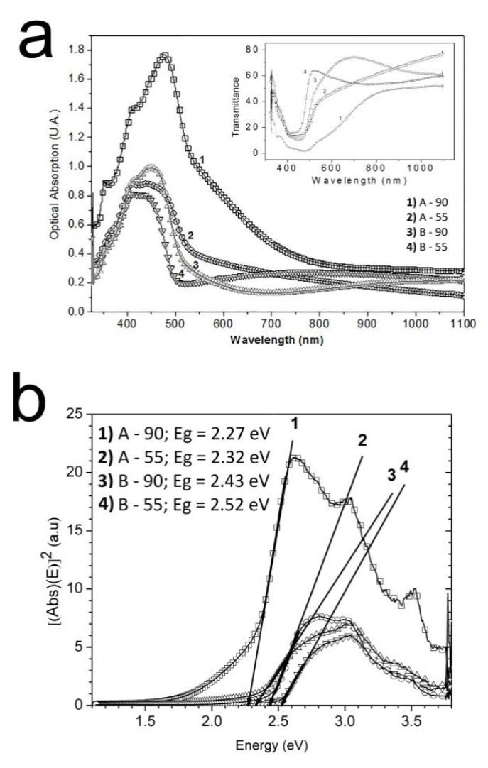
Figure 10 a) Absorbance spectra of the A-90, A-55, B-90 and B-55 samples, as well as their transmittance spectra (inset). b) Energy bandgap (Eg) calculated by using the Tauc method.
The energy band gap (Eg) was calculated using the Tauc relation [27], resulting in values of 2.27 eV, 2.32 eV, 2.43 eV and 2.52 eV for the A-90, A-55, B-90 and B-55 films, respectively (Figure 10b).
It appears that Eg was larger for lower deposition times, regardless of whether sodium citrate or ammonium chloride was used as a complexing agent. This is in agreement with the grain sizes obtained by XRD for the same samples. Regardless of deposition time, Eg values were higher for the sodium citrate formulation than for the ammonium chloride formulation. The fact that Eg became bigger with decreasing grain size can be explained in terms of quantum confinement effect that becomes stronger in nanostructured films [28].
Figure 11 shows the absorbance spectrum of copper-doped CdS film as a function of Ta. It can be seen that all samples had an absorption band centered at 490 nm, which was attributed to the surface plasmon of copper nanoparticles [29] and is consistent with the presence of copper peaks shown in XRD results.
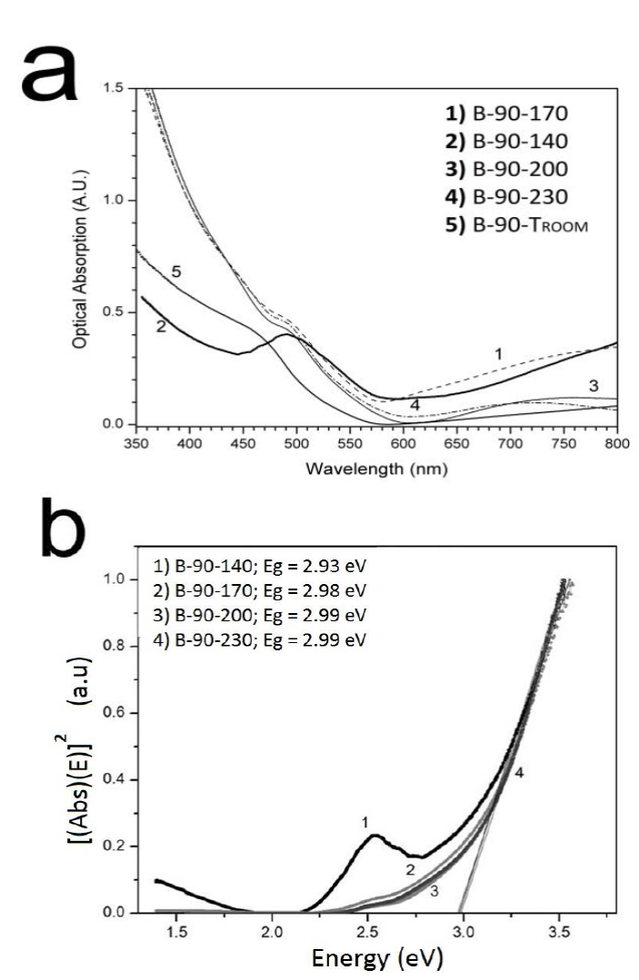
Figure 11 a) Absorbance spectra of copper-doped CdS film as a function of Ta. b) Energy bandgap (Eg) calculated by using the Tauc method.
The plasmon absorption was most intense at Ta = 140 °C, followed by Ta = 170 °C, in agreement with the relative intensities of the XRD peaks associated with cubic Cu (Figure 8). The position of the plasmon band in the absorbance spectrum is consistent with the 13-nm grain size obtained from the XRD results above.
The Eg of the B-90-Ta films was calculated as a function of Ta using the Tauc relation (Figure 11b). Eg resulted very similar for all Ta values: 2.93 eV at 140 °C; 2.82 eV at 170 °C; 3.04 eV at 200 °C; and 2.90 eV at 230 °C. The average Eg was 2.92 eV, which is consistent with a CdS crystal lattice that expands when Cu is incorporated into it, but that still preserves its cubic phase [30].
Figure 12 shows the photoluminescence spectra of CdS and Cu-doped CdS films. At first, it seems that the spectra of CdS films obtained from the sodium citrate formulation are similar to those obtained from the ammonium chloride formulation, since both present two wide emission bands in the ranges of 500 - 600 nm and 600 - 800 nm. However, a closer examination reveals that the band in the 500 - 600 nm region is asymmetric for the films prepared from ammonium chloride, but not for those prepared from sodium citrate. The band in the 600 - 800 nm region is also narrower when the ammonium chloride formulation is used. After deconvolution of the spectra, the films obtained from the ammonium sodium citrate formulation presented bands centered at 524 nm, 685 nm and 730 nm. The band centered within the energy chloride formulation presented emission bands centered at 543 nm, 580 nm and 670 nm, while those obtained from the range of 2.28 - 2.37 eV (524 - 543 nm) was present for both formulations, corresponding to a band-to-band electronic transition, and could be attributed to the bandgap energy of each corresponding film [31,32]. This is in agreement with the absorbance measurements presented above (Figure 10). The PL emission band centered at 580 nm was attributed to electronic transition from donor energy states to valence band. Donor energy states moved into the energy gap due to the presence of interstitial cadmium (Cdi) [33,34]. The emission band centered within the 1.81 - 1.85 eV energy range (670 - 685 nm) was present for both formulations and was attributed to the presence of cadmium vacancies (VCd), particularly with the electronic transition from the conduction band (CB) to VCd [34,35]. This transition could be assumed to take place in a range of 1.81 - 1.85 eV below the conduction band, implying that the VCd states are located in a range of 0.47 - 0.71 eV above the valence band, which is reasonably consistent with earlier reports [36,37]. The broad emission peak centered at 730 nm was attributed to the presence of sulfur vacancies (Vs) [31,38]. The presence of the 730 nm band in the films synthesized with sodium citrate, and its absence in those obtained from ammonium chloride, indicate that sodium citrate, but not ammonium chloride, promotes the formation of Vs. On the other hand, the presence of the 580 nm band in the films synthesized with ammonium chloride and its absence in those obtained from sodium citrate indicate that ammonium chloride, but not sodium citrate, promotes the formation of Cdi.
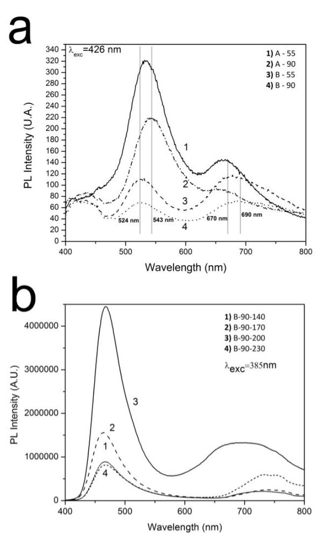
Figure 12 a) PL emission spectra of CdS films. b) PL emission spectra of Cu-doped CdS films as a function of Ta.
The relative intensity values of PL emission bands, corresponding to a band-to-band electronic transition and electronic transitions assisted by defects, show that using the ammonium chloride formulation resulted in CdS films with better optical quality (or a minor number of defects).
Figure 12b shows the PL emission spectra of the B-90-Ta films as a function of Ta. The spectra showed a blue shift of the peak associated with a band-to-band electronic transition, which is consistent with the absorbance measurements presented above, showing an increase in Eg when CdS films were doped with Cu (Figure 11). Two points are also worth mentioning about the emission band associated with crystalline defects: 1) It only shows the Vs-related emission and the VCd-related emission disappears, which is consistent with the incorporation of Cu ions into Cd sites; and 2) Its relative intensity decreases, meaning that film optical quality increases with Cu doping. Only the film obtained by using Ta = 200 °C showed the presence of VCd, although more studies are needed to clarify this finding since it was not the purpose of this study.
Conclusion
Chemical bath deposition followed by thermal annealing resulted to be a good process to synthesize CdS:Cu thin films with an electrical resistivity of 5.822 × 10⁻⁵ Ωcm, an average roughness of less than 9 nm, and an average thickness of 160 nm.
The size of the particles making up the CdS:Cu film decreases as Ta increases, starting at 160 nm at Ta = 140 °C and reaching 10 nm at Ta = 200 °C and higher temperatures.
The formulation using sodium citrate as a complexing agent resulted better to obtain nanostructured films with homogeneous chemical composition and a roughness in the nanometric range. The films behaved as an n-type semiconductor with an energy gap of about 2.38 eV that varies only slightly with deposition time and the precursors' nature, but increases to 2.93 eV with Cu doping. The lowest resistivity obtained was that of the B-90-140 film, whose nanostructured nature was composed of cubic-phase nanocrystals smaller than 10 nm, contained VCd and VS but not Cdi, and showed significant copper diffusion at 140 °C thermal annealing.
The low resistivity of 5.822 × 10⁻⁵ Ω cm obtained in this study results to be one of the lowest electrical resistivities reported for an n-type CdS film.

