


Services on Demand
Journal
Article
 English (pdf)
 Article in xml format
 Article references
 Send this article by e-mail
Indicators
-
 Cited by SciELO
 -
 Access statistics
Related links
-
 Similars in
SciELO
Similars in
SciELO
Share

 Permalink
Superficies y vacío
Print version ISSN 1665-3521
Superf. vacío vol.26 n.3 Ciudad de México Sep. 2013
Study of InxGa1-xN layers growth on GaN/Al2O3 by MOCVD at different pressures
Guarneros C.*1, Espinosa J. E.1, Sánchez V. M.2, López U.3
1 Posgrado en Física Aplicada, Facultad de Ciencias Físico-Matemáticas Benemérita Universidad Autónoma de Puebla Blvd. 14 Sur 6301, Col. San Manuel, 72570, Puebla, México * cesyga@yahoo.com.mx
2 Sección de Electrónica del Estado Sólido, Departamento de Ingeniería Eléctrica Centro de Investigación y de Estudios Avanzados del Instituto Politécnico Nacional Av. I. P. N. 2508, San Pedro Zacatenco, 07360, México, D. F.
3 Facultad de Ingeniería Química, Benemérita Universidad Autónoma de Puebla Blvd. 14 Sur 6301, Col. San Manuel, 72570, Puebla, México.
Recibido: 14 de noviembre de 2012
Aceptado: 26 de agosto de 2013
Abstract
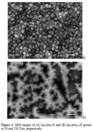
We present the InxGa1-xN layers growth in a metalorganic chemical vapor deposition (MOCVD) system. First, we growth a GaN epitaxial layer on sapphire substrate, trimethylgallium (TMGa) and ammonia (NH3) are precursors of gallium and nitrogen, respectively, and hydrogen (H2) is used as the carrier gas. Later, on the GaN epilayer, the growth of the InxGa1-xN layer is carried out using trimethylindium (TMIn) as the indium precursor. The InxGa1-xN layers were studied using X-ray diffraction (XRD) and scanning electron microscopy (SEM). XRD pattern shows the diffraction lines which could be ascribed to the formation of hexagonal In0115Ga0.885N for sample A, and In0.26Ga0.74N for sample B, both with the wurtzite type structure. SEM images illustrate the effect of the growth pressure on the films surface morphology. At low pressure the sample A has smaller grain size and higher nuclei density; at high pressure the island size increases and has lower density (sample B). The alloy formation is favored at 550 Torr.
Keywords: InxGa1-xN alloys; Growth pressure; XRD patterns; Indium concentration; Vegard's law.
1. Introduction
InxGa1-xN alloys are potential materials for the fabrication of blue/green light emitting diodes LEDs, and violet/blue injection lasers LDs, since the band gap energy of InxGa1-xN can be varied from 3.4 to 0.7 eV by increasing the InN concentration and the potential operating wavelengths cover nearly the entire visible spectral range. However, the growth of InxGa1-xN alloys using MOCVD has proven to be extremely challenging, mostly due to the trade-off between the epilayer quality and the amount of InN incorporation into the alloy as the growth temperature is changed. The low solubility of InN in GaN and the large solid phase miscibility gap phase separation and compositional inho-mogeneity are commonly observed in InxGa1-xN alloys, which may have both advantageous and detrimental effects upon the performances of the devices. Experimental observations of splitting double X-ray diffraction peaks in InGaN alloys are used to be considered as the evidence of compositional inhomogeneity [1].
According to X. L. Zhu et al. multiple diffraction peaks are observed in X-ray diffraction from InGaN layers and some caution is required when interpreting the peaks, especially a diffraction peak at about 2θ ≈ 33°, which may originate from different possible causes. The two main points of view consider the peak related to phase separation of about 50% InGaN in the InGaN alloy matrix evidenced by XRD and metallic indium nanowires in an InGaN matrix analysis. Indium penetrates through InGaN film with small lateral size of nanometers with its (101) plane parallel to (0001) InGaN surface [2, 3].
On the other hand, the indium incorporation increase significantly as the growth temperature decreased. In order to investigate the pressure effects on InxGa1-xN layer growth we carried out experiments with two different pressures, at 50 Torr and 550 Torr.
2. Methodology
InxGa1-xN layer was grown by MOCVD horizontal quartz reactor. The precursors were trimethylgallium, trimethylindium and ammonia for Ga, In, and N, respectively. The ~1 μ thick GaN templates were grown on (0001) oriented (Al2O3) sapphire substrates at 900° C prior to the growth of InxGa1-xN layers, the experimental details are given in references [4, 5]. Two different samples were grown at low temperature (600° C), the sample A was grown at 50 Torr and the sample B was grown at 550 Torr, during 30 minutes, respectively. TMGa flow rates were A) 4.4 μmole/min, B) 7.19 μmole/min, and TMIn flow rate for the two samples was 3.14 μmole/min. Ammonia flow rate was 0.5 slm, and H2 flow rate was 3.5 slm for both samples. The InxGa1-xN layers were studied using XRD and the surface morphology was studied by SEM. The indium concentration in the layers was determined from XRD patterns and the band gap was calculates using the Vegard's law.
3. Results and Discussion
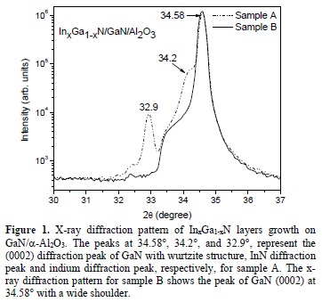
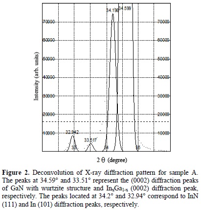
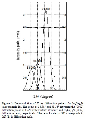
X-ray diffraction (XRD) measurements were performed using an X-Ray Diffractometer Panalytical X-Pert Pro MRD with Cu target operated at 40 kV and 20 mA. Figure 1 shows the X-ray diffraction pattern of InxGa1-xN layers, A and B, grown on GaN/α-Al2O3 templates. However, multiple diffraction peaks are observed in this x-ray diffraction patterns. Many researchers have been studied the solid phase immiscibility in InxGa1-xN, which occurs due to large difference in interatomic spacing (with lattice mismatch -11.25% between the two end binaries, GaN and InN). This immiscibility results in phase separation and growth instabilities in InxGa1-xN system [6-9]. Thus, for the two samples synthesized, it can observe the presence of the GaN and InN phases. For the sample A, the XRD peak deconvolution (Figure 2) shows the peak corresponding to GaN with wurtzite structure along the (0002) plane at 34.58° (Pattern: 00-050-0792) [10]. The peak at 34.2° comes from InN (111) (Pattern: 01-070-2563) and the peak corresponding to InxGa1-xN (0002) is located at 33.55° [2, 11]. The other diffraction peak founding in the diffractograms correspond to the In (101) incorporation at 32.9° (Pattern: 00-005-0642) [12]. The XRD peak deconvolution for sample B (Figure 3) shows the diffraction peaks for GaN (0002), InN (111) and InxGa1-xN (0002) at 34.58°, 34.0° and 33.56°, respectively. With the change in the growth pressure, sample B, the peak related to metallic indium tend to disappear. This indicates that the alloy formation is favored at high pressures (550 Torr) near to atmospheric pressure.
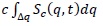
Lattice parameter determination provides information on both composition and residual strain of the films. Assuming the epitaxial film to be fully relaxed, the lattice parameter is only affected by the chemical composition. The lattice constants in the growth direction, c(GaN) and c(InGaN), for any allowed (00.1) reflection, are given directly by Bragg's law [13]:

Using radiation of wavelength λ = 1.5406 Å and with the relevant Bragg angle (θB), estimated from the XRD distribution peak. The sample A lattice constants obtained by use of Eq. (1) are c(GaN) = 5.183 Â and c(InGaN) = 5.343 Å. For the sample B, lattice constants obtained are c(GaN) = 5.185 Â and c(InGaN) = 5.335 Å.
According to the Vegard's law, a ternary alloy shows a linear dependence of lattice parameter on composition, therefore, the indium composition (x) can be derived from the plane spacing measured in one specific direction. This is obtained from the out-of-plane lattice parameter c of alloy film, by the following expression [14]:
where c0GaN = 5.1850 Å, c0InN = 5.7033 Å. Then, the compositions obtained from Eq. (2) were xA= 0.304 and xB = 0.289. It can be expressed as In0.3Ga0.7N for sample A, and In0.29Ga0.71N for sample B. These values were used for calculate the lattice constant a(InGaN) for both samples by the following equation:
where a0GaN = 3.1892 Å and a0InN = 3.5378 Å. The respective lattice constants obtained are a(InGaN)A = 3.2938 Å and a(InGaN)B = 3.2899 Å. The energy gap width is determined as a function of the local composition of the InxGa1-xN solid solution by the expression [15-17]:
Where EGaN = 3.4 eV, EInN = 0.7 eV, and b = 1.43 eV is the approximation parameter [18, 19]. The energies gap calculated are Eg(In03Ga0.7N) = 2.28 eV and Eg(In0.29Ga0.71N) = 2.3 eV.
Scanning electron microscopy (SEM) was done using a Scanning Electrón Microscope Jeol JSM 6610LV, the applied voltage was 20 kV. SEM images shown in Figure 4(A) and 4(B) illustrate the effect of the growth pressure on the films surface morphology. Sample A (50 Torr) has a smaller grain size and higher nuclei density. As the pressure is increased to 550 Torr the surface of the sample B is composed of the planar regions and by hexagonal three dimensional (3D) islands. The island size increases and has lower density, because the adatom migration decreases at high pressure. Also, the adatom migration is usually suppressed at low temperatures; the decreased mobility of surface species promotes a uniform dispersion of nuclei that can effectively cover the substrate [20].
4. Conclusions
InxGa1-xN layers growth on GaN templates by a MOCVD system were investigated at 50 y 550 Torr. Both samples have face separation. The sample growth at low pressure has the InN, InGaN and In faces. The sample growth at high pressure shows better morphological and structural characteristics, because there is no indium incorporation as metal and no droplets were formed on the surface, it is observed the island growth with hexagonal form. Also, the diffraction peak corresponding to the InN face show lower intensity compared to the diffraction peak corresponding to the InGaN face. Therefore, not only the low temperatures favor the formation of the alloy, the high pressures allow bigger indium incorporation in the GaN crystal structure too.
Acknowledgements
The authors want to acknowledgements Tec. D. Ramirez (SEES-CINVESTAV) for his technical assistance, Dr. A. Escobosa (SEES-CINVESTAV) for his support in X-ray diffraction, Dr. E. Rubio and R. Agustin (CUV-BUAP) for his support in SEM images acquisition.
References
[1] N. A. El-Masry, E. L. Piner, S. X. Liu, S. M. Bedair Applied Physics Letters 72, 40 (1998). [ Links ]
[2] X. L. Zhu, L. W. Guo, B. H. Ge, M. Z. Peng, N. S. Yu, J. F. Yan, J. Zhang, H. Q. Jia, H. Chen, and J. M. Zhou Applied Physics Letters 91, 17211 (2007) 0. [ Links ]
[3] A. Krost, and J. Bla Sing, H. Protzmann, M. Lunenburger, and M. Heuken Applied Physics Letters 76, 1395 (2000). [ Links ]
[4] Victor-Tapio Rangel-Kuoppa, Cesia Guarneros Aguilar, Victor Sánchez-Reséndiz Thin Solid Films 519, 2255 (2011). [ Links ]
[5] C. Guarneros, V. Sanchez Vacuum 84, 1187 (2010). [ Links ]
[6] P. Ruterana, G. Nouet, W. Van der Stricht, I. Moerman, and L. Considine Applied Physics Letters 72, 1742 (1998). [ Links ]
[7] D. Doppalapudi, S.N. Basu, K.F. Ludwing, and T.D. Moustakas Journal of Applied Physics 84, 1389 (1998). [ Links ]
[8] D. Doppalapudi, S.N. Basu, and T.D. Moustakas Journal of Applied Physics 85, 883 (1999). [ Links ]
[9] M.K. Behbehani, E.L. Piner, S.X. Liu, N.A. El-Masry, and S.M. Bedair Applied Physics Letters 75, 2202 (1999). [ Links ]
[10] B. Shen, Y. G. Zhou, Z. Z. Chen, P. Chen, R. Zhang, Y. Shi. Journal of Applied Physics A 68, 593 (1999). [ Links ]
[11] O. Jani, C. Honsberg, Y. Huang, J-O Song, I. Ferguson, G. Namkoong, E. Trybus, A. Doolittle, S. Kurtz; Design, Growth, Fabrication and Characterization of High-Band GaP InGaN/GaN Solar Cells, Conference Record of the 2006 IEEE 4th World Conference on Photovoltaic Energy Conversion, V. 1 p. 20 (IEEE,New York, 2006). [ Links ]
[12] B. N. Pantha, J. Li, J. Y. Lin, H. X. Jiang Applied Physics Letters 93, 182107 (2008). [ Links ]
[13] K. P. O'Donnell, J. F.W. Mosselmans, R. W. Martin, S. Pereira and M. E. White Journal of Physics: Condensed Matter 13, 6977 (2001). [ Links ]
[14] G. Xi, W. Hui, J. De-Sheng, W. Yu-Tian, Z. De-Gang, Z. Jian-Jun, L. Zong-Shun, Z. Shu-Ming, and Y. Hui Chinese Physic B 19, 106802 (2010). [ Links ]
[15] M. Kurouchi, T. Araki, H. Naoi, T. Yamaguchi, A. Suzuki, and Y. Nanishi Physica Status Solidi (b) 241, 2843 (2004). [ Links ]
[16] H. J. Kim, Y. Shin, Soon-Yong Kwon, H. J. Kim, S. Choi, S. Hong, C. S. Kim, Jung-Won Yoon, H. Cheong, E. Yoon Journal of Crystal Growth 310, 3004 (2008). [ Links ]
[17] Yen-Kuang Kuo, Bo-Ting Liou, Sheng-Horng Yen, Han-Yi Chu. Optics Communications 237, 363 (2004). [ Links ]
[18] J. Wu, W. Walukiewicz, K. M. Yu, and J. W. Ager III, E. E. Haller, Hai Lu and William J. Schaff Applied Physics Letters 80, 4741 (2002). [ Links ]
[19] C. Caetano, L.K. Teles, M. Marques, A. Dal Pino Jr., L.G. Ferreira Physical Review B 74, 045215 (2006). [ Links ]
[20] N. K. van der Laak, R. A. Oliver, M. J. Kappers, C. McAleese and C. J. Humphreys Microscopy of Semiconducting Materials: Springer Proceedings in Physics 107, 13 (2005). [ Links ]

