


Services on Demand
Journal
Article
 English (pdf)
 Article in xml format
 Article references
 Send this article by e-mail
Indicators
-
 Cited by SciELO
 -
 Access statistics
Related links
-
 Similars in
SciELO
Similars in
SciELO
Share

 Permalink
Superficies y vacío
Print version ISSN 1665-3521
Superf. vacío vol.25 n.4 Ciudad de México Dec. 2012
Morphological and optical properties of porous silicon annealed in atomic hydrogen
Coyopol A.*, Díaz-Becerril T.**, García-Salgado G., Rosendo E., Juárez H., López R., De La Rosa E., Pacio M., and Galeazzi R.
CIDS-ICUAP, Benemérita Universidad Autónoma de Puebla 14 sur y Av. San Claudio, Edif. 137, Puebla 72570, Pue. México. *acoyopol@gmail.com, **tomas.diaz.be@gmail.com.
Recibido: 13 de agosto de 2012
Aceptado: 03 de noviembre de 2012
Abstract
In this work, optical and morphological changes on hydrogen-annealed porous silicon layers (PSL) are reported. The PSL were annealed in a hot filament chemical vapor deposition (HFCVD) system at a temperature of 1000 °C. Annealing time, 10, 20, 60, 90, 180 and 360 sec was taken as parameter to changes the properties of PSL. After treatment, the samples were characterized by scanning electron microscopy (SEM), Fourier Transform infrared (FTIR) spectroscopy, reflectance and photoluminescence (PL) measurements. It was found that silicon matrix, in the PSL, was etched off by their interaction with atomic radicals causing changes in its morphology, porosity and thickness. The reflectance of the film, which is dependent on the porosity, also decreased to values near to 0% in the range of 400 to 850 nm even for short annealing times. The emission properties of the films, in the visible range, shifted to blue region for longer processing time.
Keywords: Porous Silicon; PL; FTIR; Atomic Hydrogen.
1. Introduction
Nowadays, porous silicon (PS) is a material widely used in several fields of application such as, optic, energy-photovoltaic, chemistry and biology. Properties such as compatibility with silicon-based microelectronics, low cost of obtaining, large surface area within a small volume, and the ability to modulate its refractive index as a function of depth [1] have been the subject of research. PSL are usually formed by anodizing of a silicon wafer in hydrofluoric (HF) solution and their characteristics can be modified by changing the preparation conditions used on its formation. Porosity and refractive index can be changed during the process by varying the applied current density. By this way the fabrication of multilayered structures are possible and devices among them distributed Bragg reflectors and Fabry-Perot filters can be made [2, 3, 4].
Changes in the properties of the PSL can be performed during its formation process or by means of a thermal process once the film is already obtained. Thermal annealing and thermal oxidation have been used to change the structural and emission properties of the PSL [5-9]. Techniques such as Rapid Thermal Process (RTP) [10, 11], Rapid Thermal Oxidation (RTO) [12, 13] have been used to control those properties and all compatible with the microelectronic technology. Due to the technological importance, new process to change and control the properties of the PSL are required.
In this work some results on the properties of PSL subjected to atomic hydrogen exposition are presented. It was found, the porous silicon layer was etched off as result of such exposition. As consequence, the pore size increased and its optic properties as the reflectance and PL changed. The morphology of the film reshaped from the typical dendritic morphology to sponge-like one. The emission properties showed a blue shift effect once the film was processed in atomic hydrogen atmosphere. This approach could be used to enhance or develop devices based on this type of material.
2. Experimental
The porous layers were obtained by anodization of p-type, B-doped, 0.02 ohm-cm resistivity, (100) oriented silicon wafers immersed in a solution (1:1) of hydrofluoric acid (HF: 40%) and ethanol. A density of DC current of 50 mA/cm2 was applied to obtain the porous silicon layer. The porosity of the PS samples was 48% as measured by gravimetric technique and the thickness was estimated to be 70 |am approximately. The PS samples were oxidized by exposition to room environment for two weeks after that they were placed into the HFCVD reactor, the chamber wasclosed and evacuated and the tungsten filament was heated up to 2000 °C by applying an AC voltage of 80 V between their terminals. Molecular hydrogen was flowed (50 sccm) through the hot filament to produce atomic hydrogen. The atomic hydrogen is highly reactive and it has been used for etching a solid source, usually quartz (SiO2) and silicon substrates [14-16].
The properties of the porous samples were modified varying the annealing time, 10, 20, 30, 60, 90, 180 and 360 sec while others parameters in the process were kept constant. The samples were characterized in morphology, reflectance and photoluminescence by using a scanning electron microscope (SEM) FEI Helios-Nanolab 600, an UV-Vis Thermolab system in the range of 300 to 800 nm and a photoluminescence home-made system equipped with; a laser B&E TEK (wavelength of 407 nm) and a PIN silicon photodiode as excitation and detection devices respectively. Additionally a FTIR Bruker Vector 22 was used to determine the microstructure on the samples. All measurements were performed at room temperature.
3. Results and Discussion
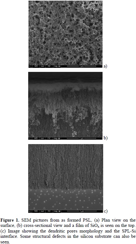
In figure (1) SEM pictures from as-obtained PSL are presented (reference sample). The plan view (Fig. 1a) reveals the existence of a mesoporous layer. The exposition of such PSL to the room environment causes the formation of silicon oxide on both on the surface and at the pores as seen in SEM cross-sectional image in Figure (1b). A more detailed image of the pore morphology, in a cross-sectional view, is shown in figure (1c). The interface of PSL-Si (substrate) can also be seen.
When the porous layer is exposed to the atomic hydrogen in the HFCVD chamber, the film morphology is modified. In figure 2, SEM images of PSL with different annealing times are presented. The figure (2a) shows the surface morphology of the reference sample. As the annealing time is increased, the surface of the porous layer is modified on both in surface and depth. Porosity of the film changes and the silicon filaments are rounded by the action of the atomic hydrogen, figures (2a) and (2b).
After 360 seconds of permanence, the porous silicon layer is completely removed and pores are no seen anymore (fig. 2d) and the surface becomes polished. It seems the atomic hydrogen reacts with the silicon atoms at the film.
In a cross-sectional SEM view, it can be seen the silicon matrix also change its morphology in the depth. A sample with 20 seconds in atomic hydrogen is shown in Figure 3(a). It can be noted a modified film with approximately 1 µm of thickness. A like chain, instead the original dendritic, morphology is observed in the upper part of the film and conformed by silicon crystals. This change can be controlled by the annealing time in the process. In figure (3b) the SEM image of a sample exposed 60 seconds to the action of atomic hydrogen is shown. In figure (3b) can be noted that the film is composed by 2 sections. A portion of the layer was modified and has a thickness of 40 um approximately and the other, under this part, the original porous film with a thickness of 15 um is seen. This image gives us evidence that the temperature of the process is no responsible for the changes observed during the exposition of the PSL to the atomic hydrogen. After 180 seconds of heat treatment, the film is completely modified. The sponge morphology can be seen clarity (Figure (3c)); however, its final thickness (30 µm) is less than that of the original layer (70 µm).

The results above can be explained by considering that the etching of silicon atoms by atomic hydrogen proceeds by the breaking of Si-Si bonds. This leads to the formation of higher surface hydrides, SiH(β1) and SiH2(β2) precursors for the formation of silanes (SiH4) as the etching product [17,18].
Porous silicon can be considered as a nanocrystalline skeleton immersed in a network of pores and having a very large internal surface area (~500 m2/cm3). This internal surface is highly reactive, the oxygen atoms react with the silicon atoms and the surface is covered with silicon dioxide even at room temperature.
When this oxidized porous silicon layer is exposed to hydrogen radicals, the silicon dioxide is removed producing silicon monoxide (SiO) and hydroxyl ions (OH) [14-16] and probably SiHx. Once the silicon surface is oxide free, the atomic hydrogen consumes silicon atoms to produce silicon precursors in gas phase (silanes are assumed) and as consequence the silicon is removed from the internal surface (figures. 1-3). The atomic hydrogen is introduced into the pores and might lead to the formation of the sponge structure as seen in figures 3(a)-3(c).
The silicon oxide etching was corroborated by FTIR measurements. Figure (4) shows the absorbance FTIR spectra from porous samples exposed to atomic hydrogen. Spectra (R) was drawn from the oxidized porous silicon layer (reference sample). It can be observed the characteristic vibration modes for the Si-O-Si bonds, stretching, bending and rocking peaked at around 1080, 800 and 460 cm-1. A band at 881 cm-1 was also observed and it is assigned to the bending mode of Si-H bonds [1921].

As the annealing time increases the number of Si-O-Si bonds decreases causing a reduction in the intensity of the stretching, bending and rocking vibrations of such bonds (curves (a), (b) and (c)). The intensity of the stretching band is more o less constant for longer treatment times and probably caused by the new native oxide formed once the sample is exposed to the room environment for measurement.
The result above shown confirms the etching of the silicon oxide at the PSL. Additional bands can be observed around 600-750 cm-1, at 635 cm-1 and a shoulder at 665 cm-1, associated to Si-H wagging y SiH2 bending vibrations respectively [22]. The above mentioned bonds could be resulted from the interaction of silicon atoms at the silicon filaments and the atomic hydrogen. Once the silicon oxide is consumed the silicon filaments are etched and the film is modified as seen from figures (2) and (3). The etching rate of porous silicon is around of 12.5 μm/min, a high rate compared to those obtained on polished silicon surfaces employed as substrates. The internal specific area of the porous layer may account for this etching rate.
Some optical properties of films subjected to the hydrogen process were obtained. As seen before, the silicon atoms in the PSL are removed when the film is exposed to atomic hydrogen. As result the percentage of porosity in the film increases. Some properties relating porosity must change. One of them is the reflectance. In figure (5) the reflectance properties from PS layers are presented. It can be noted that as the annealing time increases, the reflectance of the film reduces to values between 0 and 5 % (curves (a), (b), (c), (d)) in the range of 450-800 nm with respect to untreated PS one (8%) (curve (R)).
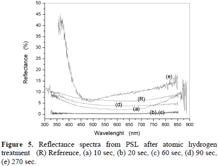
Films highly absorbents can be obtained even for samples with low treatment times (20 sec, curve (b)). The reduction in the reflectance can be due to the modification in the porosity and/or in the morphology of the film as seen in figures 2 and 3. For longer annealing times the film decreases in thickness and the reflectance value increases (curve e).
The PSL parameters were attempted to be obtained by fitting their measured reflectance spectrum, but it was no possible because of its strong optical absorption and thickness. However, for longer annealing times the PSL reduces in thickness and some constructive interferences cause oscillations in the measured reflectance as seen in figure (5), curve (e). In this case, by using the matrix method [23, 24] and the effective medium approximation of Looyenga-Landau-Lifshits [25] the porosity was determined to be 72 %. From the relation [26];
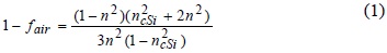
where fair is the void corresponding to the porosity of the film expressed in per cent, ncSi is the refractive index of the silicon, a value of 1.65 in the refractive index was calculated. From the results obtained, it can be pointed out that in this approach the porosity of the film and the refractive index can be controlled by adjusting the annealing time. In the present experiment the values varied from 48 % to 72 % and from 2 to 1.65 for the porosity and refractive index, respectively.
This result may be important due to its potential application as antireflective coating in solar cells. The approach can be used to improve the efficiency of the solar cells.
The evolution on the PL properties was measured and analyzed as function of the annealing time. It is well known that as grown PS layer exhibits visible emission centered at orange-red region. The origin of those phenomena is ascribed to radiative recombination of electron-hole pair (ehp) at silicon nanocrystals (Si-ncs) at the filaments of the PSL. In figure (6), the room-temperature (R-T) PL spectra from porous layers subjected to different atomic hydrogen exposition time of 20, 60 and 270 sec are presented. The emission characteristics from the as grown PSL is shown as reference. As can be seen in figure (6), the reference sample exhibits a broad band centered at 750 nm. This band shifts to the blue region once the samples are annealed. This phenomenon can be explained as follows: As the atomic hydrogen atoms interact with the silicon filaments, they become thinner and smaller silicon nanocrystals are formed during the process. For longer process time smaller crystal size are obtained. As the Si-ncs go down in size, an enlargement in their band gap occurs and the emission properties shift to the blue region.

Figure (7) might give us evidence about the existence of such silicon nanocrystals. In that figure a SEM image from PS sample with 270 seconds of treatment shows silicon filaments with thickness in the order of 3 nm. Si-ncs with size around 1 nm are ascribed as the origin of PL in the blue region [27]. Although, the mean size of such silicon-nc reduces as the treatment time increases (as deduced in figure (6)) the trend was no verified completely and more experiments are currently done to get more information.

4. Conclusions
In this work the properties of porous silicon layers after atomic hydrogen treatment were studied. The experiments were carried out in an HFCVD reactor. The annealing time was used as parameter to control the PSL properties. It was found the silicon skeleton in the PSL is etched off by atomic hydrogen ions and morphological, optical and photoluminescence properties of the film are modified.
The etching rate of the PSL was around of 12.5 µm/min a higher value than that found in silicon susbtrates. The internal specific surface area (≈500 m2/cm3) in the layer might account for this high etching rate. The porosity of the film varied from 48% to 72% and the refractive index from 2 to 1.65 as the exposition time increased. The treated PSL exhibited low values of the reflectance in the range of 0 to 5% for 450 to 800 nm. Zero reflectance was obtained even for samples subjected to low exposition time (20 sec). Due to the silicon etching in the PSL, Si-ncs could be formed and a blue shift effect was observed on the PL properties of the film once the PSL are subjected to an annealing in atomic hydrogen atmosphere. Although more experiments are needed, it is possible to control the properties of the film by this approach. The method could be used to enhance or develop devices based on porous silicon layers such as solar cell and gas sensors.
Acknowledgements
The authors like to thanks to VIEP-BUAP for the support to this project.
References
[1] Andrea Edit Pap, Krisztián Kordás, Jouko VäHäkangas, Antti Uusimäki, Seppo Leppävouri, Laurent Pilon, Sándor Szatmari, Opt. Mater., 28, 506 (2006). [ Links ]
[2] G. Mattei, A. Marucci, V. A. Yakovlev, and M. Pagannone, Laser Phys. 8, 755 (1998). [ Links ]
[3] Mark B. H. Breese and Dharmalingam Mangaiyarkarasi, Opt. Express, 15, 5537 (2007). [ Links ]
[4] M. Ghulinyan, C. J. Oton, G. Bonetti, Z. Gaburro, and L. Pavesi, J. Appl. Phys., 93, 9724 (2003). [ Links ]
[5] A.E. Pap, K. Kordás, G. Tóth, J. Levoska, A. Uusimäki, J. Vähäkangas, and S. Leppävuori, J. Appl. Phys. 86, 041501 (2005). [ Links ]
[6] Yukio H. Ogata, Naoki Yoshimi, Ryo Yasuda, Takashi Tsuboi, Tetsuo Sakka, Akira Otsuki, J. Appl. Phys., 90, 6487 (2001). [ Links ]
[7] N. Ott, M. Nerding, G. Muller, R. Brendel, H. P. Strunk, J. Appl. Phys., 95, 497 (2004). [ Links ]
[8] Yue Zhao, Deren Yang, Dongsheng Li, Minghua Jiang. Materials Science and Engineering B. 116, 95 (2005). [ Links ]
[9] X. Y. Hou, G. Shi, W. Wang, F. L. Zhang, P. H. Hao, D. M. Huang, and X. Wang. Appl. Phys. Lett., 62, 1097 (1993). [ Links ]
[10] Zhao Yi, Yang Deren, Lin Lei, and Que Duanlin. Chinese Sci. Bull., 51, 2696 (2006). [ Links ]
[11] A.J. Kontkiewicz, A. M. Kontkiewicz, J. Siejka, S. Sen, G. Nowak, A. M. Hoff, P. Sakthivel, K. Ahmed, P. Mukherjee, S. Witanachchi, and J. Lagowski. Appl. Phys. Lett., 65, 1436 (1994). [ Links ]
[12] Gu-Bo Li, Liang-Sheng Liao, Xiao-Bing Liu, Xiao-Yuan Hou, and Xun Wang. Appl. Phys. Lett., 70, 1284 (1997). [ Links ]
[13] D. I. Kovalev and I. D. Yaroshetzkii, T. Muschik, V. Petrova-Koch, and F. Koch. Appl. Phys. Lett., 64, 234 (1994). [ Links ]
[14] A.Coyopol, G. García, T. Díaz, E. Rosendo y H. Juárez. Superficies y Vacío. 23, 147 (2010). [ Links ]
[15] P. Salazar, F. Chavez, F. Silva-Andrade, A. V. Ilinskii and N. Morales, Modern Phys. Lett. 15, 756 (2001). [ Links ]
[16] T. Diaz-Becerril, G. Garcia-Salgado, A. Coyopol, E. Rosendo, H. Juarez, Mater. Sci. Forum, (636-637), (2010) 444. [ Links ]
[17] Yi Wei, Lian Li and I. S. T. Tsong, Appl. Phys. Lett., 66, 1818 (1995). [ Links ]
[18] D. R. Orlander, M. Balooch, J. Abrefah and J. Siekhaus, J. Vac. Sci. Technol. B, 5 1404 (1987). [ Links ]
[19] A.Morales, J. Barreto, C. Domínguez, M. Riera, M. Aceves, J. Carrillo, Physica E. 38, 54 (2007). [ Links ]
[20] Zhenrui Yu, M. Aceves, J. Carrillo, Mat. Sci. in Semic. Process. 7, 2004 45. [ Links ]
[21] G. Lucovsky and D. J. Tsu, J. Vac. Sci. Technol A, 5, 2231 (1987). [ Links ]
[22] S. Kalem and M. Rosenbauer. Appl. Phys. Lett., 67, 2551 (1995). [ Links ]
[23] F. L. Pedrotti, L. S. Pedrotti, Introduction to Optics, 2nd. Edit. Prentince-Hall Inc., (New Jersey, E.U., 1993). [ Links ]
[24] J. I. Cisneros, Ondas Electromagnéticas Fundamentos y aplicaciones. Libro de Texto, EDUNICAMP (Campinas SP, Brasil, 2001). [ Links ]
[25] O. Bisi, Stefano Ossicini, L. Pavesi, Surf. Sci. Rep., 38 (2000) 1-126. [ Links ]
[26] C. Pickering, M.I.J. Beale, D.J. Robbins, P. J. Pearson, R. Greef, Thin Sol. Films, 125, 157 (1985). [ Links ]
[27] M. H. Nayfeh, N. Barry, J. Therrien, O. Akcakir, E. Gratton, and G. Belomoin, Appl. Phys. Lett. 78, 1131 (2001). [ Links ]

