


Services on Demand
Journal
Article
 English (pdf)
 Article in xml format
 Article references
 Send this article by e-mail
Indicators
-
 Cited by SciELO
 -
 Access statistics
Related links
-
 Similars in
SciELO
Similars in
SciELO
Share

 Permalink
Superficies y vacío
Print version ISSN 1665-3521
Superf. vacío vol.25 n.3 Ciudad de México Sep. 2012
Optical characterization of Te-doped GaxIn1-xAsySb1-y epitaxial layers grown by liquid phase epitaxy
Bravo-García Y. E., Zapata-Torres M.
CICATA-IPN Unidad Legaria. Av. Legaria 694, Col. Irrigación, México D.F. 11500. México.
Rodríguez-Fragoso P., Mendoza-Alvarez J.G.
Depto. de Física, Cinvestav-IPN Apdo. Postal 14-740, México D.F. 07000. México.
Herrera-Pérez J. L.
UPIITA-IPN Av. I.P.N. 2580, Col. Barrio la Laguna Ticoman México D.F. 07340. México.
Cardona-Bedoya J. A.
Depto. de Física. Universidad del Tolima. Ibague. Colombia.
Gómez-Herrera M. L.
Facultad de Ingeniería. Universidad Autónoma de Querétaro Querétaro, Qro. México.
Recibido: 17 de diciembre de 2011
Aceptado: 12 de abril de 2012
Abstract
A set of GaxIn1-xAsySb1-y quaternary layers were grown on (100) GaSb substrates using the liquid phase epitaxy technique (LPE). These layers were doped with tellurium and were characterized by Raman, Photoluminescence (PL) spectroscopy, and Secondary Ion Mass Spectroscopy (SIMS). Several optical modes were identified by performing Raman spectroscopy characterization at room temperature and observing the effect of the impurity concentration on the Raman mode frequencies. From secondary ion mass spectrometry the concentrations of Te in the liquid solutions and the electron densities present in the layers were obtained. Finally, these last results were compared with those obtained from low temperature photoluminescence spectroscopy measurements at low temperatures on this set of samples.
Keywords: III-V semiconductors; Liquid Phase Epitaxy.
1. Introduction
Antimony-based III-V compound semiconductors such s GaInSb, AlGaAsSb, GaInAsSb and InAsPSb have been studied because they are the basis for the development of optoelectronic devices such as photodiodes, lasers, photodetectors, solar cells, thermophotovoltaic cells, etc., which perform in the infrared medium range [1-5]. These devices are being employed in areas such as medicine, environmental monitoring, and optical communications, among others [6-7].
In particular, the band gap energy of the GaInAsSb quaternary alloys can be tuned in the range between 1.7 to 2.3 μm, and it is possible to obtain them with a good crystalline lattice match between layer and substrate using either GaSb, InP or InAs substrates. These types of layers have been grown using technique such as Molecular Beam Epitaxy (MBE), Metal Organic Chemical Vapor Deposition (MOCVD), and Liquid Phase Epitaxy (LPE) techniques [8-11]. However, the growth of these semiconductor alloys is complicated because a broad immiscibility region is present for this type of alloy [8, 9].
Using the liquid phase epitaxy technique, it has been possible to grow these GaInAsSb layers with a high degree of crystalline quality [12]. To get this, it is fundamental that the growth parameters involved in the growth process, such as growth temperature (Tc), supercooling temperature (Tsc), and cooling rate (rc), must be optimized in order to get epitaxial layers with a high degree of crystalline quality and a lattice mismatch with the GaSb substrate as small as possible.
In this work we describe the characterization done in a series of Te-doped GaInAsSb quaternary layers grown on GaSb substrates by LPE with different Te concentrations. From this characterization we were able to obtain the layer stoichiometry, the density of Te doping in each layer, and the effect of the doping on the sample crystalline quality.
2. Experimental Details
Quaternary GaInAsSb epitaxial layers were grown in a three-zone furnace in a H2-atmosphere, using a horizontal graphite sliding boat. As substrates, (100) GaSb wafers mechanically polished from Firebird, Inc. were used. All the precursors elements used to prepare the growth melt were of 6N purity, and GaAs came from a wafer. For the intentional doping of the GaInAsSb epitaxial layers, small quantities of the Sb3Te2 alloy were added to the growth solution.
After the charge of the substrate in the boat, the temperature was raised at 640°C for one hour, in order to eliminate the oxide in the substrate surface. Then, the temperature was decreased to stabilize the system, and a cooling ramp at a rate of about 0.3 °C/min was established, after which the layers were grown at temperatures around 530 °C.
Elemental chemical microanalysis measurements were performed using a scanning electron microscope (SEM) FEI-Quanta 3D FEG model equipped with a X-ray dispersive energy microanalysis system (EDX). High resolution X-ray diffraction (RXHR) measurements were performed in the quaternary layers using a Panalytical XPERY MRD model. The atomic concentration of the dopant, Te, was determined by using a secondary ion mass spectrometer (SIMS) from CAMECA, model ims 6f, with a Cs primary ion beam. Raman spectra were recorded at room temperature using the 6328 Å line of a He-Ne laser as the exciting source. Photoluminescence (PL) measurements were done at a temperature of 15 K, using the 488 nm line of an Ar+ laser as the exciting source.
3. Results and discussions
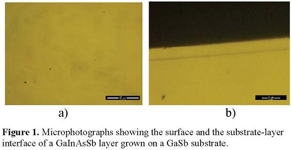
Sample thickness was determined using an optical microscope on the layers previously treated with an etching to reveal the interface substrate-layer; in all cases, the layer average thickness was around 3 microns. In Figure 1 it can be observed the microphotographs of the layer surface, as well as the substrate-layer interface.
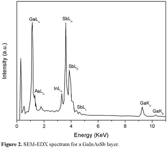
In Figure 2 it is shown an EDX image showing the composition for one of the quaternary layers; we found only the elements present in the precursor elements. From EDX characterization it was determined that the stoichiometry of the quaternary layers. For all the samples we obtained: Ga0.85 In0.15 Sb0.85.
From the results obtained in the RXHR measurements it was obtained that the lattice mismatch between substrate and layer, (Δa/a), was in the order of 4.5 x 10⁻⁴ for all samples.
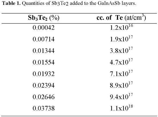
In order of incorporate different concentration of Te atoms on the samples, small quantities of Sb3Te2 were added to the growth solution. Secondary Ion Mass Spectroscopy were used for determinate the Te concentration in each sample. In Table 1, we presented the concentration of the Te atoms, for each Sb3Te2 percentage in the growth solution. We found a monotony increase if the Te atoms with respect the increase of % Sb3Te2.
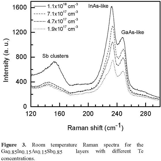
In Figure 3 it is shown the room temperature Raman spectra of the Te-doped Ga0.85In0.15As0.15Sb0.85 at different Te concentrations. It can be observed the presence of three peaks at Raman frequencies of 235cm-1, 249 cm-1 and a broad band peaked between 145 and 155 cm-1 The first two are due to the InAs-like LO mode, and the GaAslike LO mode [13]; and the last one can be correlated to the presence of free carriers due to the presence of Sb clusters [14]. The slight shoulder observed at the low frequency side of the InAs-like band is attributed to InSb-lke LO modes [13].
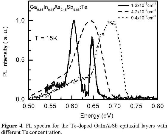
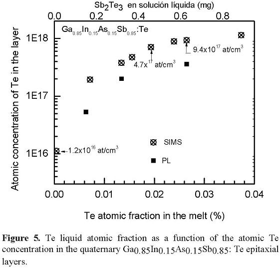
The normalized photoluminescence (PL) spectra for the three Te-doped GaInAsSb epitaxial layers are shown in Figure 4. For the sample with a Te concentration of 1.2x1016 cm-3, there is a free electro-to-acceptor transition centered at about 614 meV, which is dominant in the PL spectrum; and another PL band peaked at around 653 meV due to a bounded-exciton recombination. For the GaInAsSb sample doped with a Te concentration of 4.7x1017 cm-3 there appears a PL broad band centered at about 646 meV due to the high concentration of carriers. For the highest Te-doped sample, with a Te concentration of 9.4x10¹⁷, we observe a broad PL band shifted to higher energies peaked around 689 meV, which shifts to higher energies because of a band-filling effect [15]. A shift to higher energies of the PL band is observed as the Te concentration in the quaternary layers increases.In Figure 5 are shown the Te liquid atomic fraction obtained from the SIMS measurements, as a function of the Te concentration in the GaInAsSb layers. The filled square symbols correspond to the data obtained from the PL measurements adjusted to the band-filling model [16]. The electron concentration measured through the low temperature PL spectra and fitting the PL peak with the band-filling model, which takes into account the shift of the Fermi energy towards the conduction band as the donor concentration increases, shown a good agreement with the results obtained with the SIMS measurement. These results suggest that the Te atoms incorporated to the samples was electron donors.
4. Conclusions
High crystalline quality GaInAsSb:Te epitaxial layers were grown on (100) GaSb substrates by the LPE technique. Several growth parameters were varied in order to optimize the quality of the layers and the quality of the substrate-layer interface in such a way as to obtain the lowest values possible of the lattice mismatch parameter.
Using SIMS measurements it was possible to obtain the concentration of the Te dopant used to control the electrical conductivity of the samples. These SIMS results were compared to the electron concentration measured through the low temperature PL spectra and fitting the PL peak energy with the band-filling model which takes into account the shift of the Fermi energy towards the conduction band as the donor concentration increases. A shift to higher energies of the PL band is observed as the Te concentration in the quaternary layers increases. A good agreement was obtained from the comparison of the results from SIMS and PL.
Room temperature Raman spectra showed the presence of two bands coming from the InAs-like LO Phonon with higher intensity, and from the GaAs-like LO phonon.
Acknowledges
We acknowledge the financial support of Conactyt and ICyTDF. YEBG acknowledges a Conacyt scholarship. The technical support of Dr. Alberto Andraca and Dr. Hugo Martinez from the Center on Nano and Microtechnologies of the IPN in the characterization of the RXHR and SEMEDS measurements is also acknowledge.
References
[1]. H.K. Choi and S.J. Eglash. Applied Physics Letters 59, 10, (1991). [ Links ]
[2]. A.K. Srivastava, J.C. deWinter, C. Caneau, M.A. Pollack and J. Lyskind. Applied Physics Letters 48 ,14 (1986). [ Links ]
[3]. E. Tournié, J.L. Lazzari, E. Villemain, A. Joullié, L.Gouskov, M. Karim and I. A. Salesse. Electronics Letters 27,14 (1991). [ Links ]
[4]. M. Ahmetoglu (Afrailov), B. Kucur. I.A. Andreev, E.V.Kunitsyna, M.P. A. Mikhailova, Yu.P. Yakovlev. Infrared Physics & Technology 53, 399 (2010). [ Links ]
[5]. Michael G. Mauk. Survey of Thermophotovoltaic (TPV)Devices, in Mid–Infrared Semiconductor Optoelectronics, Springer Series in Optical Sciences, (Springer-Verlag, London,2006) pp 673. [ Links ]
[6]. B.L. Carter, E. Shaw, J.T. Olesberg, W.K. Chan, T.C. Hasenberg and M.E. Flatté. Electronics Letters. 36, 15 (2000). [ Links ]
[7]. M.P. Mikhailova, N.D. Stoyanov, O.V. Andreychuk, K.D.Moiseev, I.A. Andreev, Y.P. Yakovlev and M.A. Afrailov. IEE Proceeding Optoelectronics 149 (1) Mid-infrared optoelectronics: Materials and devices. [ Links ]
[8]. M.J. Cherng, H.R. Jen, C.A. Larsen, G.B. Stringfellow, H.Lundt and P.C. Taylor. Journal of Crystal Growth 77, 408 (1986). [ Links ]
[9]. E. Tournié, F. Petard and A. Joullié. Journal of Crystal Growth 104, 683 (1990). [ Links ]
[10]. D.S. Cao, Z.M. Fang and G.B. Stringfellow. Journal of Crystal Growth 113, 441 (1991). [ Links ]
[11]. T.H. Chiu, J.L. Zyskind and W.T. Tsang. Journal of Electronic Materials 16, 1 (1987). [ Links ]
[12]. A.K. Srivastava, J.C. deWinter, C. Caneau, M.A.Pollack and J.L. Zyskind. Applied Physics Letters 48 ,14 (1986). [ Links ]
[13]. R. Cuscó, E. Alarcón-Lladó and L. Artús. Physical ReviewB 81, 195212 (2010). [ Links ]
[14]. J. Diaz-Reyes, E. Lopez-Cruz, J.G. Mendoza-Alvarez, S. Jimenez-Sandoval. Journal of Applied Physics 100, 123503 (2006). [ Links ]
[15]. S. Iyer, S. Hegde, A. Abul-Fadl, K.K. Bajaj, W. Michel. Physical Review B 47, 1329 (1993). [ Links ]
[16]. J. Diaz-Reyes, J.A. Cardona-Bedoya, M.L. Gomez-Herrera, J.L. Herrera-Perez, I. Riech and J.G. Mendoza-Alvarez. J. Physics: Condensed Matter 15, 8941 (2003). [ Links ]

