


 text new page (beta)
 English (pdf)
 Article in xml format
 Article references
 Send this article by e-mail
 Cited by SciELO
  Similars in
SciELO
Similars in
SciELO 
 Permalink
1 Introduction
Almost 40 years ago, the rediscovering of surface plasmon polaritons (SPPs) opened an interesting possibility to fabricate photonics sensors [1-4]. SPPs are transverse magnetic (TM) polarized optical surface waves that propagate along a metal-dielectric interface. In the first experiments, the propagation distance in SPPs reached a few microns, depending on the choice of metal at the air-metal interface, and the operating wavelength [5]. Later on, it was demonstrated that it was possible to increase the propagation distance by several orders of magnitude, by reducing the thickness of the metal layer and sandwiching into a dielectric-metal-dielectric arrangement [6], this new type of SPP was call as long-range SPP (LRSPP).
Despite the improvement on the propagation distance that could be achieved, LRSPP-based devices reached their potential in sensing applications until they become active, by adding contacts to the metal stripe in order to apply an electrical current to the contacts [7]. The role of the electric current circulating through the metal stripe is to heat up the matrix in which the waveguide is embedded, thus inducing an effective change in the refractive index distribution in the vicinity of the waveguide. This, in turn, can induce significant phase accumulation that can be used for high-sensitivity sensing. By using this principle, different devices have been proposed and experimentally developed [8-16].
In this paper, we study the phase change dependence of the applied electrical current when the electric stripe is on top of the device. We propose this configuration trying to reduce the optical transmission losses caused by the heat electrical power. Our results will be useful to study the optical dependence on new LRSPP configurations. In section 2, we explain the generalities of the micro-fabrication process of the samples. In section 3, we provide our experimental results. Finally, in section 4, we present the conclusion of our work.
2 Fabrication Sample
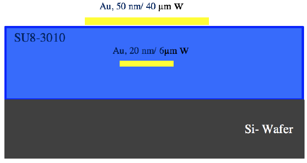
The sample was prepared on a piece of a silicon wafer which was first cleaned by using deionized water, acetone, methanol, and isopropanol. After cleaning it, a 10 μn-thick layer of photoresist SU8-3010 was deposited by using a spin coating at 3000 RPM for 45 s. Once it was cured, the surface was prepared by a 1-minute descum with a plasma-enhanced chemical vapor deposition (PECVD; Plasma-Therm 790 Series). Later, we deposited a 1 μm-thick layer of photoresist 1000 PY (-) using a spin coater at 4000 RPM during 40 s.
The sample was soft baked at 150 °C for 1 min and then exposed to UV light for 18 s at an incident power density of 12 mW/cm2 using the proper mask to delineate the metal stripe waveguides. After UV exposure, the sample was baked at 100 °C for 1 min, and the channels were revealed by immersing the sample into RD-6 resist developer for 11 s. Once the channels for the waveguides were open, Cr(1 nm)/Au(20 nm)/Cr(1 nm) were sequentially deposited by thermal evaporation (Edwards Auto 306 with quartz crystal thickness monitor). The bottom chromium layer is needed to improve the adhesion of the gold layer, and the top chromium layer is deposited to maintain the symmetry of the metal layers. The final width of the strips was 6 μm. After the metal evaporation, a standard lift-off process was used to remove the remaining metal on top of the negative photoresist while leaving only the metallic waveguides.
To obtain a symmetric waveguide, the upper cladding was fabricated by spin-coating undiluted SU-8 3010 at 3500 rpm for 40 s to obtain a thickness of 10 μm. This layer was also baked at 95 °C for 7 min and then exposed to UV light for 12 s at an incident power of 12 mW/cm2, and an identical descum process improved its surface adhesion. A second 1 μm-thick layer of photoresist 1000 PY (-) was deposited using a spin coater at 4000 RPM during 40 s, which able to record, by lithography, a Cr(5 nm)/Au(50 nm) strip 40 μm width. Finally, we use a standard lift-off process to remove the remaining metal, leaving only the metallic electric contacts on top.
A schematic of the transverse cross-section of the sample is shown in Fig. 1. The sample was fabricated such that the electrical resistance could be measured between the ends of each strip, i.e., along with the waveguide and along the electrode. The optical waveguide (20 μm width) is symmetrically embedded into the SU8 matrix. The use of this configuration will become evident in the next section.
3 Experiments and Results
In order to characterize the performance of the device, both transmission and interferometric experiments were carried on. In both experiments, the pads located at the end of the electric strip (50 μm width; Fig. 1) were connected to electrodes and electrical current circulated through contact itself. This allows placing the heat source at the top contact and produces an outwards heat flow (from the top contact to the bottom cladding). This will modify the initially isotropic refractive index distribution around the waveguide, by making it more asymmetric as the structure of the LRSPP, including the substrate, reaches thermal equilibrium.
In this way, the inherent asymmetry of the temperature distribution at equilibrium produced by the different layers in the substrate can be inferred by measuring its impact on the propagation regime of the device, i.e., short- or long-range. In the former experiment, the transmission through both the dual contact passive LRSPP was measured at a fixed wavelength as a function of the electrical power using the experimental setup shown in Fig. 2.
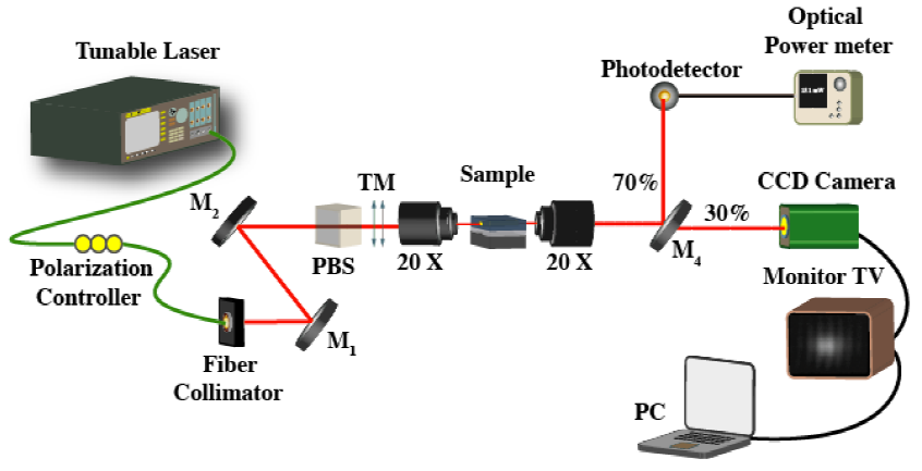
Fig. 2 Experimental set up for monitoring the dependence of the optical power transmission through the LRSSP device as a function of the electrical power applied to the contact
The tunable laser (Hewlett Packard model 8164A) was fixed at a wavelength of 1550 nm, and full polarization control was implemented to ensure having only TM polarized light. The light was coupled to and from the sample with 20X microscope objectives. The output beam was then split into two beams (70/30 BS) for simultaneous measurement of the optical power and imaging of the output intensity distribution.
The optical power was measured with an infrared photodetector (Newport 918D-IR-OD3) and a power meter (Newport 1916-C), while the output intensity distribution was imaged onto a charge-coupled device array (CCD camera, Electronics Microviewer model 7290 A).
Fig. 3 shows the optical power transmitted through the device optical waveguide (6 μm width; Fig. 1) as a function of the electrical power dissipated by the contact itself. We want to emphasize that the waveguides have a total length of 5.4 mm. In the experiment, the control variable is the electrical current flowing through the contact waveguide and, for calculating the corresponding value of electrical power, the value of resistance measured for the contact, have 1.226 kΩ for the sample, was used. The electrical power was systematically increased until full attenuation was achieved (considering its resistance). The maximum electrical current was 15.5 mA, for a maximum power of 295 mW. The current was increased at a constant rate of 0.5 mA/min, while the total transmission losses are almost 30 dB (from -6.5 dB to -35 dB) when the electrical power varies from 0 to 295 mW.
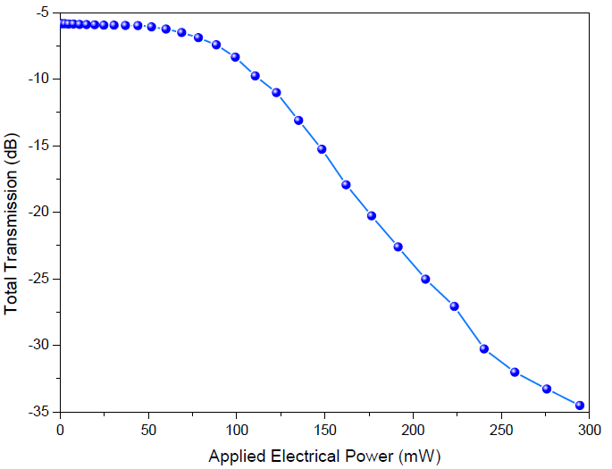
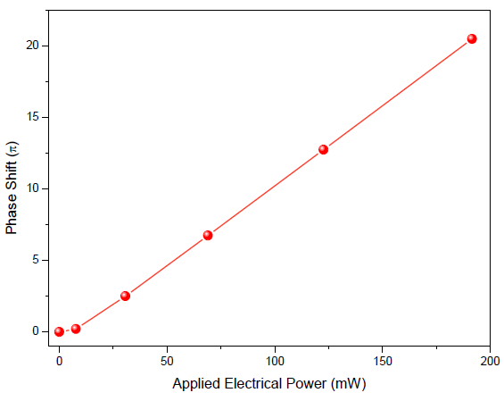
Fig. 3 Graph of the total optical transmission dependence of the applied electrical power to the contact LRSSP sample
In a second experiment, the phase change that the LRSPP induces is measured interferometrically as a function of the applied electrical current by placing the device in one arm of a Mach-Zehnder interferometer (MZI), as is shown schematically in Fig. 4. Again, 20X microscope objectives are used to couple light to and from the waveguide under test, and two 50/50 beam splitters are used at the input and output of the MZI. The interference pattern, i.e., fringes was projected onto the camera and recorded for further processing and analysis as the electrical power is increased. The range of applied power is similar but slightly shorter than that in the above experiment since the visibility of the fringes is to be ensured.
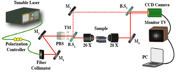
Fig. 4 Mach-Zehnder interferometer experimental set up to estimate the phase difference induced by the optical waveguide in the LRSSP device as a function of the electrical power applied to the contact
The phase shift, in units of π, as a function of the electrical applied power is shown in Fig. 5. As the electrical applied power is incremented, the temperature of the device also increases resulting in a shift of the interference pattern due to a change in the effective refractive index that the light 'sees' as it propagates through the waveguide. The change in the effective refractive index is determined mainly by the large negative value of the thermo-optic coefficient of the polymer matrix. Nevertheless, there are other effects involved such as the phase introduced by the asymmetry influence the overall response [17]. This reveals a second aspect of the asymmetric structure that can be understood in terms of an effective thermo-optic coefficient (TOC) exhibited by the overall structure as the suspended core device [18].
When a metal is heated through induction, many phenomena contribute to the change of the dielectric function response, such as the maintenance of the temperature dependence of the phase shift due to the high positive TOC, considering the real part. This is an interesting feature that allows accessing the underlying interplay between the geometry of the structure and the properties of the materials involved.
On this device, the temperature distribution is taken to a more symmetric configuration by isolating the LRSPP from the substrate in addition to a gold contact with this, the temperature dependence is significantly reduced by the presence of a substrate with TOC of opposite sign to that of the matrix in which the waveguide is embedded at the expense of sacrificing the symmetry of the refractive index distribution.
4 Conclusion
In reference with an optical beam which is being propagated through our LRSSP waveguide device, we have shown that this configuration also has a dependence of the optical power transmission and the induced phase in the optical waveguide for the electrical current applied to the contact. The proposed configuration has an acceptable electric work region from 0 to 100 mW, which able us to obtain an 11 π phase difference with a low loss of about 2 dB.
We can see from [18] that the present configuration can drive higher electrical power with a small optical loss if we compared this sample to the Non-Suspended Structure where the electrical power is applied through the optical waveguide. We assume that there are several effects involved in the device. One of them is the change in the effective refractive index is determined mainly by the significant negative value of the thermo-optic coefficient of the polymer matrix, but the asymmetric structure could play an important role in these devices.

