


 text new page (beta)
 English (pdf)
 Article in xml format
 Article references
 Send this article by e-mail
 Cited by SciELO
  Similars in
SciELO
Similars in
SciELO 
 Permalink
1. Introduction
For the improvement of very large scale integration devices (VLSI), circuit miniaturization is a great challenge for researchers [1-3]. Indeed, reducing the dimensions of MOSFETs to the nanometric scale poses problems. For example, increased power consumption and electric fields in the MOSFET channel can cause barrier rupture and therefore higher leakage currents which can damage the device. With the advancement in technology, CMOS has been manufactured [4]. However, reducing the size of the MOS transistor leads to fundamental physical effects: short channel effect [5], gate oxide and high field effects [6,7]. These issues have led to the exploration of possible successor technologies with greater scalability potential, such as single electron device (SET) technology [8-11]. SETs have recently gained a lot of attention because of their nanoscale ultra-low power dissipation [12-16]. Despite these interesting properties, the SET has integration limits. The principal problem is that the operation of a SET at room temperature requires extremely small island capacities, thus which in practice means a smaller than nanometer island size for room temperature operation [17]. The second major problem with single electron electronic components is randomness of the background charge. Indeed, a single charged impurity trapped in the insulating environment polarizes the island, creating on its surface an image charge of the order of e. This load is effectively subtracted from the external load [18]. Hybridization of SET with CMOS technology has emerged as a promising candidate for the next generation ultra-small [19-21], low-power, high-speed Nano device. To understand the characteristics of SET-based circuits and explore its applications, simulation and modeling of this device has become of great importance [22-25]. SET simulation in general is based on three approaches, analytical modeling [26], macro-modeling [27] and the Monte Carlo method [28]. In this work, we proposed a hybrid SET-NMOS logic inverter macro-model using Simulink MATLAB. NMOS is used in our model due to some inherent performance advantages [29]. Such as the mobility of electrons, which are the carriers in the case of an n-channel device, is about two times greater than that of holes, which are the carriers in the p-channel PMOS device. Thus an n-channel NMOS device is faster than a p-channel PMOS device. This paper is structured as follows. In Sec. 2, we propose a hybrid of SET-CMOS logic macro-model. The simulation results are discussed in this Sec. 3. The overall work is concluded in the last section.
2. Design of the proposed model of hybrid SET-CMOS logic
SET are three-terminal switching devices. A schematic structure and equivalent circuit of a SET is shown in Fig. 1, where the source (S), the drain (D) and the gate (G) are the three terminals. The two tunnel junctions, their corresponding tunnel resistance and capacitances, are also illustrated.

Note that Rd is the resistance of the drain tunnel junction, Rs is the tunnel resistance of the source, Cd is the capacitance of the drain tunnel junction, Cs is the capacitance of the source tunnel junction and Cg is the capacitance of the gate. The two tunnel junctions are created by a Coulomb island or Quantum dot (QD), that electrons can only enter by tunneling through one of the tunnel junctions.
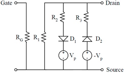
The gate terminal is capacitively coupled to the node between the two tunnel junctions. The capacitor may seem like a third tunnel junction, but it is much thicker than the others so that no electrons can tunnel through it. The capacitor simply serves as a way of setting the electric charge on the coulomb island. In our model of hybrid SET-MOS logic, the equivalent circuit of an SET is shown in Fig. 2. The charge energy changes periodically depending on the gate bias. This energy is included in the resistors R1, R2 and R3. which are expressed as follows [30]:
And
where CR1, CR2, CVp, CI2 and CF1 are different parameters used to adjust the input and output current-voltage characteristics.
The inverter model proposed in Fig. 3, designed by Simscape, consists of an NMOS, whose source is connected to ground, and a SET macro-model that replaces the PMOS. A square input signal of 0 to 5 V is applied as input voltage to the common gate of the NMOS and SET.

The purpose of the two combinations R2, V1, D1, and R3, V2, D2 is to obtain an adequate current onset in the positive and negative directions for different values of Vds.
3. Simulation results
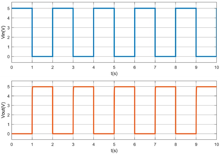
Figure 4 shows the simulation results of the designed circuit. The input signal Vin and output signal Vout are shown in the same figure. The signal obtained at the output changes depending on the value of the input signal, these characteristics are given in Fig. 4. When the input voltage of the gate is low, NMOS is activated and SET is deactivated. For this reason, a high output voltage is obtained. Similarly, when a high input voltage is applied to the gate terminal, opposite phenomena occur and a low output voltage is obtained at the output terminal.
The power consumed by the hybrid SET-CMOS logic proposed is given in Table I. By comparing the performance of the designed SET-CMOS logic hybrid circuit with its CMOS logic counterpart in terms of energy consumption.We deduce that the power consumption is less in Hybrid CMOS-SET logic technology (35.59 nW) than CMOS logic technology (120.4 nW).
4. Conclusions
The macro-modeling of SET accompanied with CMOS gives a new direction in the evolution of research work on nano devices. The proposed inverter, replacing the PMOS by the SET macro-model, has a new hybrid SET-CMOS logic architecture, which offers ultra-low electrical power dissipation, high response speed and also improved operation in the low voltage region. The performance of the proposed inverter is verified by simulation in Matlab Simulink's Simscape environment, which is capable of efficiently simulating hybrid SET-CMOS logic circuits on a very large scale. The results obtained are promising enough to increase its reliability and to justify the use of the model in the design of ultra-dense electronic logic circuits.

