


 text new page (beta)
 English (pdf)
 Article in xml format
 Article references
 Send this article by e-mail
 Cited by SciELO
  Similars in
SciELO
Similars in
SciELO 
 Permalink
1. Introduction
SnS thin film is a tin chalcogenide semiconductor in group IV-VI with an orthorhombic structure of eight atoms per unit cell that forms biplane layers normal to the greatest c-axis. Due to fully saturated intra layer covalent bonds and a system of unit layer interactions dominated by weak Vander Waals forces, SnS exhibits a two-dimensional structure.
Because of the pressures arising from the force action, the lattice match has a less substantial effect on the crystallinity of the film. SnS meets the basic criterion of a semiconductor material for use in transistors as semiconductor channel layers, as solar absorbers in thin film solar cells, and in other electronics and optoelectronics devices due to its narrow band gap, structural properties, electrical properties advantage, and acceptability from the standpoint of cost, availability, stability, and toxicity free [1-3].
The regulation of thin film thickness is crucial in SnS thin film semiconductor processing [4]. Due to the large number of small grains with large quantities of grain boundaries acting as an electron trap, pinholes, voids in a separate island-like state, and traps associated with certain film thickness affect charge carriers, affecting the electrical conductivity/properties, optical energy band gap, and threshold voltage for use in optoelectronics and electronics devices.
Deposition techniques used for SnS thin films include chemical bath deposition [5-7], Electrochemical deposition [8], thermal evaporation [9], Spray Pyrolysis [10], Sputtering [11], Atomic layer deposition [12] and chemical vapour deposition [13] among others. The resulting SnS thin films from these processes could often have disordered growth due to substantial concentrations of grain boundaries and pinholes, resulting in materials defect, among others with peculiar advantages and disadvantages.
3D printing, on the other hand, is a new deposition process that turns a computer model into a three-dimensional item. In recent years, 3D printing technology has advanced at a breakneck pace, gaining new uses outside of its usual sectors [14-16]. It is the direct manufacture of components via layer-by-layer deposition guided by digital information from a computer-aided design file. Liquid deposition modeling (LDM) and Fused deposition modeling (FDM) are two current 3D printing technologies.
FDM includes heating a thermoplastic filament to a semiliquid condition, then extruding and depositing it onto a substrate using a nozzle to manufacture parts layer by layer depending on CAD file information [17]. Despite its ease of usage with a wide range of materials, the FDM has limitations when it comes to thermoplastic polymers.
By allowing the use of conductive paste, functional, and liquid precursors for thin film deposition/fabrication, the LDM overcomes the limitations imposed by the FDM [15,18]. The LDM deposition mechanism is such that the pressure system pushes out the materials to be deposited through the extruder such that the flow of material is controlled alongside the retraction to interrupt deposition with a defined pressure force and movement speed.
The 3D printing of thin film was recently reported for thin film deposition [19-21]. We report for the first time the use of 3D printer to deposit SnS thin film using the liquid deposition modelling (Solution printing) and the investigation of the SnS film layer/thickness variation for application in electronics and optoelectronic devices.
2. Materials and method
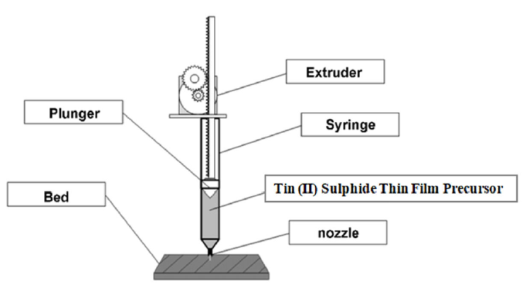
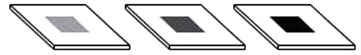
3D model and number of laid down layers (one (1), two (2), and three (3)) of the SnS thin films were designed using AUTODESK FUSION 360 computer aided design. Based on the slice information, the 3D printer manufactured the parts one layer at a time, stacking and combining succeeding layers to create the appropriate 3D printed SnS thin film layers. The CAD models were sliced using an Ultimaker Cura virtual environment on a laptop computer connected to the 3D printer to create a two-dimensional (2D) slice stack. SnS semiconductor thin films were printed on soda lime glass substrate using Tin chloride dehydrates and Thiourea as precursors which was prepared as previously reported [3] after which the resulting solution was used for 3D printing using a modified Cartesian 3D printer on the substrate by spray deposition. The substrate was placed on the print bed during printing while the printing was done at a deposition temperature of 258°C. The 3D printer is a modified Cartesian 3D printer. The schematic diagram of the deposition process is shown in Fig. 1 while the schematic of 3D layer pattern for printed SnS thin films is shown in Fig. 2.
The carrier density, carrier mobility and conductivity type of the films were determined by an ECOPIA Hall Effect measurement system (HMS 3000 Hall measurement system) based on Van der Pauw configuration. Surface Profilometer, Energy dispersive X-ray spectroscopy, Scanning Electron Microscopy (SEM), four point probe, X-ray diffractometer and a UV Spectrophotometer was used to determined the thickness of the films, elemental composition of the film, morphology of the SnS thin films and the optical parameters in the range of 200 to 1100 nm wavelength.
The average crystallite size (D) of the SnS thin film was calculated using:
where θ = diffraction angle, λ = wavelength of the X-rays (1.5406 Å) and β = full width at half maximum (FWHM).
Dislocation density δ was calculated using [2]:
The micro-strain ε was evaluated using [22].
where D, β and θ retain their meanings as defined for Eq. (1).
The absorption coefficient α (alpha) was calculated from [23]:
The optical band gap E g and absorption coefficient are related by the Tauc plot as [24] where the symbols retain their usual meaning:
The optical energy band gap (E g ) of SnS thin films was obtained by extrapolating a straight line from the (αhv)2 vs optical band gap energy plots to the (αhv)2 = 0 axis, where the intersection point gives the optical band gap.
3. Results and discussion
The results and discussion of the various characterisations/measurements of the SnS thin film material is presented as follows.
3.1. Surface profilometer
Surface Profilometry estimates the thickness of the 3D printed SnS thin films to be 0.2 μm, 0.4 μm and 0.6 μm for 1, 2, and 3 layers, respectively. The liquid deposition modeling 3D printer’s deposition method is based on a mechanical or pneumatic system in which pressure pushes materials through the extruder. It is thus feasible to precisely control the flow of materials as well as the retraction to prevent deposition using the appropriate pressure force and movement speed. The additive aspect of 3D printing allows the heat in a printed layer to be retained for a longer time, allowing and enhancing the addition of additional materials/SnS thin film layers for thickness variation and layer leveling. This allowed for easier printing/deposition of SnS thin films, similar to the heated chamber, and lower power usage when compared to other deposition/manufacturing methods that used a highly heated bed and air heater. Better heat preservation enhances thin film layer adhesion while air contaminants are removed, resulting in improved print quality and material structure.
3.2. Energy dispersive xray spectroscopy (EDS)
The EDS spectra of a 3D printed SnS thin film with thicknesses of 0.20, 0.40, and 0.60 μm for 1, 2, and 3 layers is shown in Fig. 3 while Fig. 4 illustrate the error bar with a standard deviation of 3.29. The existence of other minor peaks, which could be connected with trace levels of Silicon (Si), Calcium (Ca), Oxygen (O), Chlorine (CI) and Sodium (Na), from the substrate utilized for the film deposition, was identified in the films. Similar observation has been reported by [2]. Sulphur concentration rose as film thickness increases, as shown in Table I.
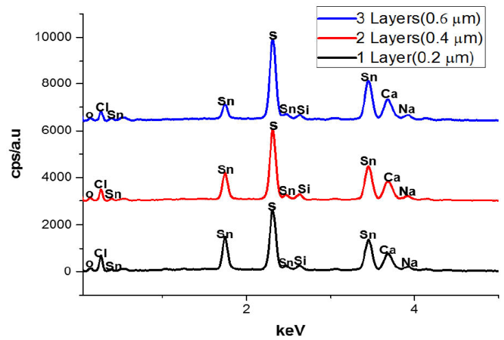
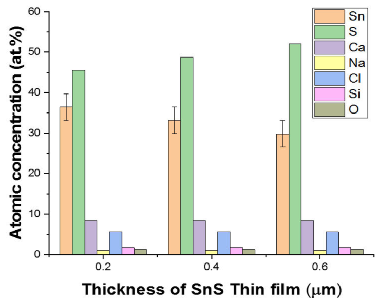
Table I 3D printed SnS thin film composition (at.%).
| Thickness (μm) | Sn (at.%) | S (at.%) | Ca (at.%) | Na (at.%) | Cl (at.%) | Si (at.%) | O (at.%) | TOTAL 100 |
|---|---|---|---|---|---|---|---|---|
| 0.20 | 36.43 | 45.57 | 8.35 | 1.04 | 5.62 | 1.74 | 1.25 | 100 |
| 0.40 | 33.19 | 48.81 | 8.35 | 1.04 | 5.62 | 1.74 | 1.25 | 100 |
| 0.60 | 29.85 | 52.15 | 8.35 | 1.04 | 5.62 | 1.74 | 1.25 | 100 |
Because Sulphur is of a higher vapour pressure than Tin, more Sulphur atoms tend to arrive on the substrate for SnS thin film formation than Tin atoms, as shown in Table I. Sulphur atoms appear to be reflected back at the substrate surface in single-layer SnS thin films, which could be as a result of the reduced sticking coefficient and adsorbed-atom mobility between the surface of the substrate and the thin film, leading to a decreased Sulphur concentration. However, when the thickness of the SnS thin film and layers grows on layers deposition, the effect diminishes due to a reduction in scattering, resulting in a reduction in thermal gradient and the formation of SnS crystallite clusters.
3.3. X-ray diffractometer (XRD)
Figure 5 shows the XRD pattern of SnS thin films with one layer (0.20 μm), two layers (0.40 μm), and three layers (0.60 μm) scanned across a 2 theta angle of 20 ° to 80 ° range.
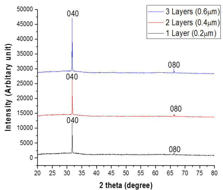
The peaks in the SnS thin films were examined and indexed using the orthorhombic structured SnS pattern, which is the conventional pattern for the mineral herzenbergite (JCPDS PDF card 39-0354).
The XRD pattern of the films shows that a crystalline film with few peaks has formed. The respective SnS thin films showed large peaks at 2 theta angles of 31.7 ° and 66.6 ° diffracted along the planes (040) and (080), showing an increase in the intensity of films with increasing film layer/thickness, which is unique to the chalcogenide poorly crystalline or nearly amorphous network. Table II shows the structural parameters of the films.
The average size of the crystallites was found to rise with increase in thickness. As demonstrated by the dislocation density and micro strain, this helps the production of developed atomic layers, which generates a thermal energy gain system of atomic restructuring, resulting in a rise in crystal size and a decrease in crystal defects in SnS thin films.
The low crystal size of 54.94 nm for the 1 layer SnS thin film of 0.2 μm thickness could be as a result of a reduction in the growth of printed SnS film atoms due to a nuclide formation depreciation caused by a lack of bonding and material between the substrate layer and the nuclides, which could limit charge carrier mobility.
Nucleation on the other hand, increases as the number of SnS film layers/thickness and the interactions with the substrate surface decreases, resulting in the merger of smaller crystallites into larger ones due to the potential energy gap between the particles. Similar results have been reported [25-26]. Increasing the film layer increases the size of crystallite by forming larger grains in the preceding printed layer (s) by the process of simultaneous annealing due to layer(s) addition.
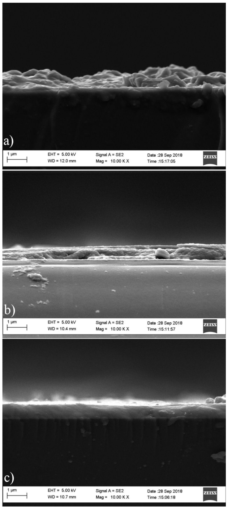
3.4. Scanning electron microscopy
Figure 6 shows the morphology of the 3D printed SnS thin films as determined by scanning electron microscopy a)-c). The cross sectional image of the printed films is shown in Figs. 7a)-c). The grain size of the films was determined using imagej [2,27]. The SEM morphology and cross sectional result reveals two distinctive microstructures consisting of a section of spherical grains and agglomerates. The films contain more uniform and closely bound grains as the film thickness increases to 2 layers and 3 layers, with the 0.60 m film having the most enhanced grain and crystal structure, with the inner layers of the film atoms being exposed to greater inter atomic forces, resulting in the formation of a defined compact structure [28]. The increase in printed layers allowed the growth of smaller grains into larger grains that as a result of the coalescence of the grains. The average grain sizes are 90.01, 140.29 and 156.30 nm for 1 layer, 2 layers and 3 layers respectively.
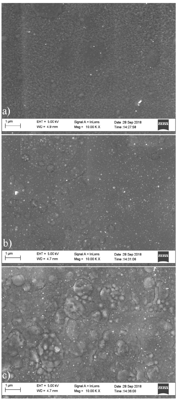
Figure 6 a) Surface morphology of 3D printed SnS thin film of 3 layer (0.60 μm thickness). b) Surface morphology of 3D printed SnS thin film of 2 layers (0.40 μm thickness). c) Surface morphology of 3D printed SnS thin film of 1 layer (0.20 μm thickness).
3.5. Four point probe and Hall effect measurement
The electrical conductivity of the 3D printed SnS thin films as with film thickness is shown in Fig. 8. The electrical conductivity was found to be 0.001754, 0.002684 and 0.002987 (Ωm) -1 for 0.2, 0.4 and 0.6 μm thickness. The Average Hall coefficient RH obtained are 2.22 × 10³ (m3/c), 2.43 × 10³ (m3/c) and 2.74 × 10³ (m3/c) for SnS thin film of 0.20, 0.40 and 0.60 μm thickness respectively. Since the average Hall coefficient of all the samples were positive it signifies that all the films exhibit p-type carrier conductivity.
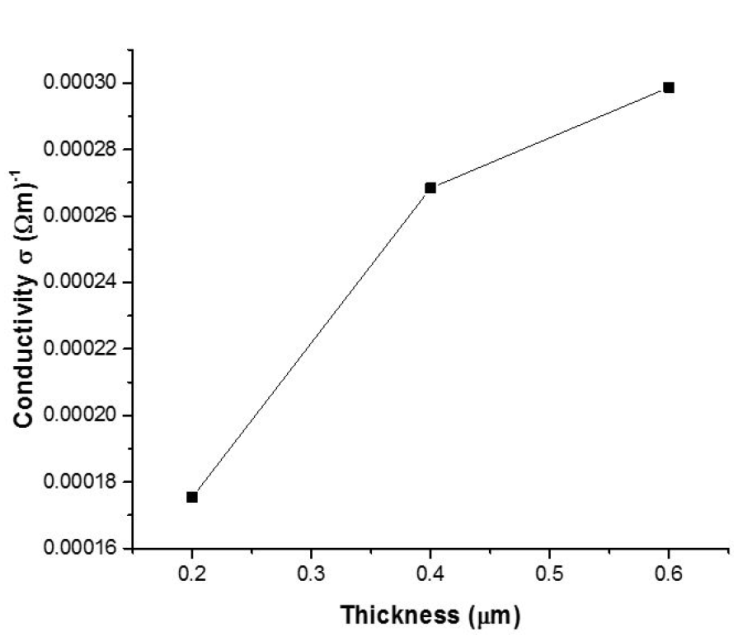
Several researchers have demonstrated that lattice defects, residual stress, and grain size affect the electrical conductivity of formed SnS thin films [29-30]. According to the XRD and EDS data, there are no binary phases of the film, and stress is minor, but the grain size grows as the thickness increases. As a result, the grain size of the films had a substantial role in the variation in electrical conductivity with thickness. Indicating that the decrease in electrical conductivity is attributable to decline in the material’s structure defects. As the film thickness is increased, the film crystallinity improves steadily, resulting in a more uniform structure with larger grains.
Larger grains could lower the trap carrier density, thereby enhancing the carrier passage through the lattice which leads to increase in conductivity. Thinner films, such as the 0.2 μm SnS thin film, have defect that operate as scattering centers, potentially increasing the occurrence of trap states capable of trapping the quantity of free carriers accessible for conduction. The carrier traps get electrically charged after traping mobile carriers, providing a potential energy barrier that inhibits charge carriers mobility thereby reducing carrier mobility and the number of free carriers available for conduction [26,30].
3.6. Spectrophotometer-optical energy band gap
Figure 9a)-c) show the Tauc plots of SnS films of 0.20, 0.40 and 0.6 μm thickness from where the band gap of the SnS films were estimated.
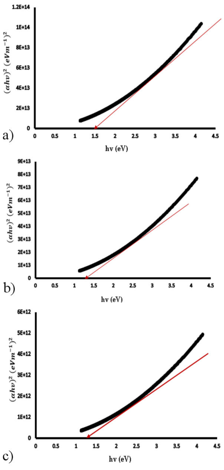
For all of the films, a linear relationship of (αhv)2 with hv was observed, indicating direct band gap and showing that the SnS thin films are of direct transition at all thicknesses investigated. Figure 8 shows that the band gap decreases from 1.51 eV for 0.20 μm thickness to 1.46 eV for 0.40 μm thickness and 1.37 eV for 0.60 μm thickness.
According to the XRD results, the decline in band gap with thickness is due to an increase in grain size and a large density of dislocations. [3,31-34] have also reported similar trend. Thinner films have been reported to exhibit higher transmission in the lower wavelength range, implying that the absorption edge changes with wavelength, resulting in a bigger band gap, as seen in 0.2 μm film [35].
The increase in crystallite size for thicker films could explain the decrease in optical band gap energy with thickness. With increasing thickness, the adsorption atom mobility rises, resulting in an increase in crystalline nature and a decrease in the energy band gap [32]. The drop in E g with thickness can also be explained by an increase in localised density of states towards the band margins, which lowers E g [36].
Because the band gap approaches the photovoltaic solar energy conversion optimum, the optical energy band gap of 1.37 eV of 0.6 μm 3D printed SnS thin film is optimal and favors attainment of the threshold voltage for electronics and optoelectronic applications.
4. Conclusion
The 3D printing of SnS thin film was achieved using the liquid deposition modelling 3D printing technology. Surface Profilometer, EDX, XRD, SEM, Uv-vis spectrophotometer, Hall effect measurement and four point probe were used to characterise the thickness, elemental composition, structural, morphological, optical and electrical properties of the SnS thin films. The system allows the heat in a printed layer to be preserved for a longer time which allows and enhances the addition of other layers of the materials thin film for thickness variation, layer levelling and easy printing, like in the case of the heated chamber and lower power consumption in comparison with powerfully heated bed and air heater in other deposition techniques. This aid the formation of higher print quality and material structure as better heat preservation improves thin film layer adhesion with air impurities removal due to the absence of air in a vacuum. The 3D printed SnS films were found to consist of Sn and S elements confirming the presence of SnS thin film. SnS thin films of 1, 2 and 3 layers of 0.2, 0.4 and 0.6 μm thickness were printed on soda lime glass substrate. The SEM result reveals the presence of uniform and homogenous printed films devoid of cracks. The XRD patterns reveals the formation of crystalline film with peaks. Increasing the film layer increases the size of crystallite by forming larger grains in the preceding printed layer(s) by the process of simultaneous annealing due to layer(s) addition. The increase in film thickness facilitates the formation of grown atomic layers that creates a thermal energy gain system which enhances atomic restructuring leading to an increase in the crystal size and a decrease in crystal defects in the SnS thin films as revealed by the dislocation density and the micro strain. A p type conductivity of 0.002987 (Ωm) -1 and optical energy band gap of 1.37 eV of 0.6 μm, 3D printed SnS thin film is optimum and favours the attainment of the threshold voltage for optoelectronic and electronic application as the optical band gap also approaches the photovoltaic solar energy conversion optimum. The electrical conductivity can be enhanced with annealing and doping of the SnS film with suitable dopants. The solution printing method of the liquid deposition modelling employed has the advantage of been able to print solution that contains polymer matrixes and inorganic fillers in intricate geometrics of materials composites. The results demonstrates the technological potential of the emerging three dimensional printing of thin film for materials synthesis, deposition and device application as it offers the advantage of materials saving via mass customisation, reduced fixturing and tooling and rapid fabrication of complex geometric structures.

