SciELO - Scientific Electronic Library Online

 
vol.68 issue3Microscopic spin orbit analysis for proton+9Be scatteringOptical response of dielectric&metal-core/metal-shell nanoparticles: Near electromagnetic field and resonance frequencies author indexsubject indexsearch form
Home Pagealphabetic serial listing  

Services on Demand

Journal

Article

Indicators

Related links

  • Have no similar articlesSimilars in SciELO

Share


Revista mexicana de física

Print version ISSN 0035-001X

Rev. mex. fis. vol.68 n.3 México May./Jun. 2022  Epub Apr 14, 2023

https://doi.org/10.31349/revmexfis.68.031301 

Research

Optics

First-principles investigations of electronic and optical properties of Er-doped GaN involved in ErGaN/ErN quantum well heterostructures

S. Amiria 

K. Agrouib 

B. Amiric 

M. Abboun Abidd 

A. Belghachie 

aDepartment of Electrical Engineering, Laboratory Simulation, Commanded, Analysis and Maintenance Electrical Network, National Polytechnic School of Oran-Maurice Audin, BP 1523 El Mnaouer, Oran, Algeria.

bSemiconductors Technology for Energetic Research Center (CRTSE) BP 140 Alger-7 Merveilles Algeria.

cHigher Normal School of Bechar, Algeria.

dNational Polytechnic School of Oran-Maurice Audin, BP 1523 El Mnaouer, Oran, Algeria.

eBechar university Tahri Mohamed, BP 417 Bechar, Algeria.


Abstract

We study the electronic, the optical and the transport properties of both bulk materials ErN and Er0.125Ga0.875N, which crystallize in zinc-blind and wurtzite structures, respectively, and are utilized in quantum well devices. The properties are calculated using density functional theory (DFT), by applying the full-potential linearized augmented plane-wave (FP-LAPW) method with a spin-orbit coupling effect. The analysis of the electronic properties shows that ErN and Er0.125Ga0.875N have a band gap at 0.79 and 3.38 eV, respectively. On the other hand, the technology makes it possible to stack these materials for a quantum well heterostructure of Er0.125Ga0.875N/ErN. The optical properties such as optical coefficients, refractive index and extinction coefficient are discussed in detail. The transport properties of alloys are investigated using the semi-classical Boltzmann theory as implemented in the BoltzTraP code in conjunction with ab initio electronic structure calculations. Our findings suggest that Er doping of wide band gap semiconductors could be a viable option for quantum well devices.

Keywords: RE:III-N quantum well GGA+U BoltzTrap

1. Introduction

Semiconductors are used in the vast majority of modern electronic devices. As a result, plenty of research is being conducted to improve their electronic and optical properties with this ever-increasing number of available materials; it is becoming increasingly important to predict the optical properties of new materials in order to determine their usability in optoelectronic devices such as semiconductor lasers or solar cells [1]. III — N compounds are direct band gap energy (Eg) ranging from 0.7 eV for InN, 3.42 eV for GaN, and 6.2 eV for AlN. They can be used at high-temperature, high-frequency, and high-power microelectronic devices. In particular, the GaN is an excellent compound, due to its thermal stability, high thermal conductivity, strong bonding, and distinguished structural, physic-chemical properties [2]. Of particular importance from theoretical and experimental viewpoints, BBiN and Gd doped III — N have been studied in detail by Sam et al., and Amiri et al., respectively [3, 4]. These materials hold enormous promise in optoelectronic and spintronic applications. The electronic configuration of each lanthanide RE element is often denoted as [Xe]4f n, where [Xe] is the electronic configuration of xenon and n is the number of electrons in the inner 4f shell. When incorporated into a host material, the RE atom tends to form a trivalent ion (RE3+). An interesting aspect of these compounds is the occurrence of localized strongly correlated 4f electrons, the treatment of which presents a challenge to band-structure theory [5]. The incorporation of rare-earth elements into III — N is of significant interest for different industrial applications because of their temperature independence and stable emission together with the possibility of optical or electrical excitation [6, 7]. Rare-Earth elements doped III — V are arguably among of the most studied in optical-electronic devices using principles of band gap engineering and quantum confinement. Their applications spanning from a laser, light-emitting diode (LED), vertical-cavity surface-emitting lasers (VCSELs), and quantum-confined Stark effect (QCSE) [8]. The cause of energy loss by transmission or thermalization of photons is related to the shift between the incident solar spectrum and the band gap of most solar cells. The photon conversion strategies such as downconversion, upconversion, and downshifting are possible technologies to increase the efficiency of solar cells. In this regard, trivalent lanthanide ion-doped luminescent materials have attracted great interest due to their promising application as spectral converters [9, 10, 11]. Er-doped III — N materials have been investigated using different growth methods such as ion implantation; Steckl et al. [12] have reported on the fabrication of GaN-based display materials doped with various high concentrations of rare-earth ions and have fabricated electroluminescent devices by molecular beam epitaxy (MBE). Altahtamouni et al.[13], have synthesized Er-doped GaN quantum well structures by metal organic chemical vapor deposition (MOCVD) [13]. This was the motivation for the theoretical study of electronic, optic, and transport properties of both bulk materials heterostructure ErGaN/ErN where the barrier and well crystallize in wurtzite and zinc-blind structure, respectively. Our calculations are based on the GGA+U method with a spin-orbit coupling effect. The structural band, optical parameters, and transport properties are calculated. The rest of the paper is organized as follows: Section 2 provides a brief overview of the computational method used. The detailed electronic properties are discussed in Sec. 3.1. Section 3.2 goes over the optical properties and 3.3 discusses transport properties. Finally, Sec. 4 concludes the paper.

2 Computational details

We have investigated the electronic, optical and transport properties of ErN and ErGaN bulk materials shown in Fig. 1, based on DFT [14, 15] using the FP-LAPW method [16, 17] as implemented in the Wien2k code [18]. To calculate the exchange correlation potential, the GGA+U approach wasutilized with a spin-orbit coupling effect, we have used the Hubbard potential U = 8 eV and J = 0 eV for 4f electrons of Er as already reported by Harmon et al. [19], and modified Becke-Jonson approximation (mBJ) [20]. The wurtzite structure of GaN contains 16 atoms, 8 atoms of Ga and 8 atoms of N, one atom of Ga was substituted by one Er atom, to obtain the ErGaN corresponding to a doping concentration 0.125 % of Er. The wave functions are expanded into planes waves in the interstitial region with a cut-off K max = 8 / RMT where RMT has the smallest of all MT sphere radii and K ma is the plane wave cut-off structures ErN and ErGaN we used 2000 and 200 K-points, respectively, in the irreducible Brillouin Zone (IBZ) for our calculation. The BoltzTraP code [21] was used to calculate thermoelectric (TE) properties from ab-initio data using the semi-classical Boltzmann transport theory within the constant relaxation time and rigid band approximations.

Figure 1 Unit cells of ErN and Er0.125Ga0.875N.  

3 Results and discussion

3.1 Electronic properties

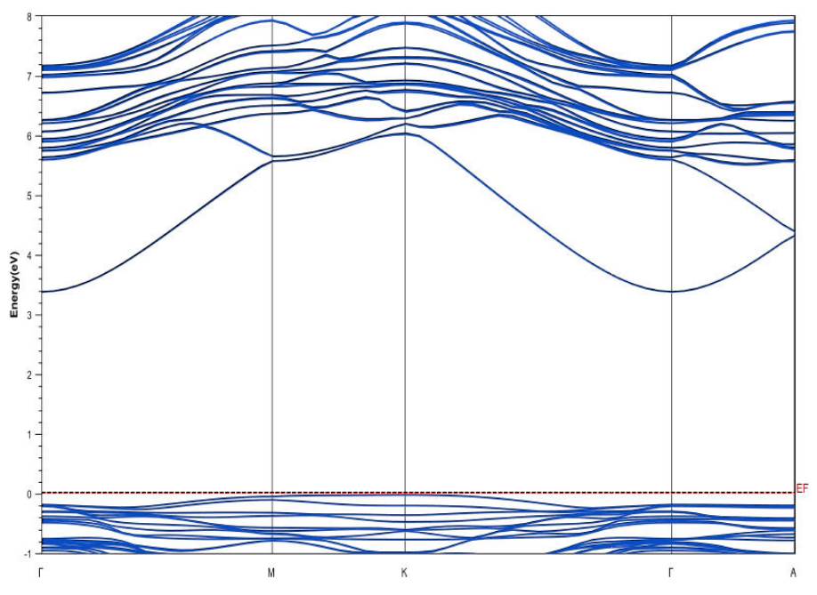
It is interesting to note that ErN turns out to be a semiconductor for the majority spin based on the band structure shown Fig. 2. An indirect band gap at 0.79 eV, with the valence band maximum (VBM) can be seen at point Γ and the conduction band (CBM) at point X in the spin-orbit coupling effect with the Hubbard approach. On the other hand, the electronic band structure of Er0.125 Ga0.875N is shown in Fig. 3, the VBM is located at point K and CBM at point Γ of the Brillouin zone, which means that we have an indirect band gap at 3.38 eV using the GGA + U approach and a spin coupling effect, which is in good agreement with Filhol et al., [22] in wurtzite and in contrast with cubic structures found by Lantri et al.[23] and Lazreg et al.[24]. Er0.125Ga0.875N is, consequently, considered as a semiconductor. The band gap values with different approaches are depicted in Table I.

Table I Band gap for ErN and Er0.125Ga0.875N materials with different approximations. 

Materials Approximation Eg(eV)
GGA 0.000 (Metal)
ErN GGA+U 0.418
mbJ +U+ so 0.790
Other calculation 0.97 [25]
GGA 0.666
Er0.125Ga0.875N GGA+U 3.477
mbJ+U+so 3.380
Other calculation 3.109[23]

Figure 2 Band structure of ErN with GGAmbJ+U+so approximations. 

Figure 3 Band structure of Er0.125Ga0.875 N with GGAmbJ+U+so approximations. 

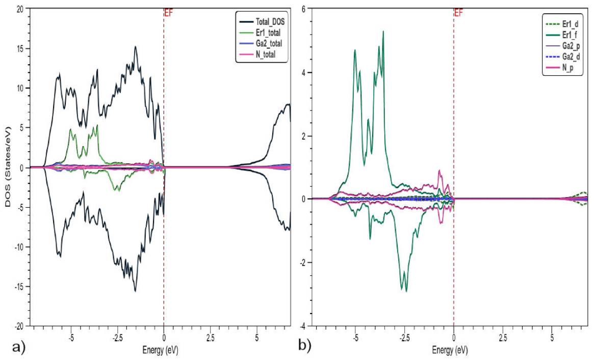
Total and partial spin polarized density of states of ErN are shown in Fig. 4. The valence bands are dominated by the 4f shell of Er states in the region ranging from -9 to -7.5 eV and by the 5p shell of N states from -.35 to -1.5 eV. The bottom of the conduction band is dominated by 4f in range 4.5 to 5.5 eV. For the total DOS, the valence band is dominated by majority spin; in contrast, the conduction band is dominated by minority spin. The DOS of Er0.125 Ga0.875N is shown in Fig. 5, with the 4f shell of Er being dominant and the Ga 4p shell overlapping with the N 5p shell in the valence band. Conversely, the 4p, 5p and 4f shell overlap in the conduction band.

Figure 4 Total and partial density of states of ErN with GGAmbJ+U+so approximations. 

Figure 5 Partial density of states of Er0.125Ga0.875N with GGAmbJ+U+so approximations. 

3.2 Optical properties

The dielectric function describes the linear response of a material to a certain electromagnetic radiation wavelength or photon energy, which relates to the interaction of photons with electrons. Other optical properties can be derived from the complex dielectric function [26]. The following study is carried out using the formalism of Ehrenreich and Cohen, where the complex dielectric function can be written as

ϵr(ω)=ϵ'r(ω)+iϵ''r(ω), (1)

ϵr'ω=1+2πP0ω'ϵr''ω'ω'-ω2dω' (2)

ϵr''ω=2ωπP0ϵr'ω'ω'2-ω2dω' (3)

where ω is the integration variable, P represents the Chauchy principal value of the integral. Similarly, one can relate the real and imaginary parts of the polarizability, namely,

nω=1+2πP0Kω'ω'-ωdω' (4)

and

Kω=2πP0Kω'ω'-ωdω' (5)

The absorption coefficient α (E) is given by

α(E)=4πλK(E), (6)

where λ is the wavelength of light in vacuum.The real part of the optical conductivity is calculated according to the following relation:

σ(ω)=ω4πϵ(ω). (7)

The most important property of a quantum well (QW) is the absorption coefficient, which can be written as

α(ω)=e2m*2ϵ0ϵrcnrLm02P2ωn,mgvm|gcnΘ(Emn-ω), (8)

where n,m gvm|gcn is the overlap integral between the z-dependent envelope functions of a conduction band and valence band, L is the width of quantum well, Θ is the Heaviside step function, nr is the refractive index of the well material, and P is defined as P=Ncellψkc*(r')pAψkv(r')d3r'. For a quantum well, χn(z)=2/Lsin(nπz/L), and (8) can be recasted in the form

α(ω)=2πe2ϵ0ϵrcnrm*2V1ω×i,j|i|pz|j2|δ(Ej-Ei-ω)(fFDi-fFDj), (9)

where i and j are the initial and final states and f FD is the Fermi-Dirac distribution function. For two consecutive states, Eq. (9) may be written as:

α(ω)=2πe2ϵ0ϵrcnrm*2V183L2×i,jδ(Ej-Ei-ω)(fFDi-fFDj), (10)

and Eq. (10) can be put into the from

α(ω)=nsπe22ϵ0ϵrcnrm*Lf21δ(ΔE-ω). (11)

Here n s is sheet charge density and f 21 defines oscillator strength from the first to the second state. The total absorption coefficient of QW is the sum of confined states α w and free states continuum α b approximated by the barrier absorption coefficient given as follows [27, 28]:

αTot=αw(ω)+αb(ω). (12)

This parameter is calculated by combining two numerical techniques; the first describes the optical properties for both materials (ErN, Er0.125Ga0.875N) using the Wien2k package with GGAmBj+ U including a spin-orbit coupling effect, and the second consists in optical properties of QW [29, 27]. Figure 6a) shows the results of the absorbtion coefficient; we noted increasing absorption trends of ErN and Er0.125Ga0.875N while changes in absorption during energy range 0-14 eV. For ErN, the absorption begins at a slightly lower energy, 0.8 eV (1550 nm). It is worth noting that absorption for Er0.125Ga0.875N begins at 3.4 eV (365 nm), which covers a large portion of the solar spectrum. The variation of the optical conductivity is shown in Fig. 6d), where begins to increase and arrives at a maximum of at 2 eV for ErN and 8 eV in Er0.125Ga0.875N for both (xx) and (zz) directions. The evolution of the refractive index and extinction coefficient are shown in Fig. 7. We note that the static refractive index of ErN is 2.3; it begins to increase until reaches its maximum at 2.8 and for Er0.125Ga0.875N, the static refractive indices are 2.9 and 2.4, it shows an increase until it reaches its maximum at 4 and 3.4 for (xx) and (zz) directions. Thus, the extinction coefficient starts to increase from a threshold equal to 2.6 eV for ErN and 3.0 eV for ErGaN in (xx) and (zz) directions.

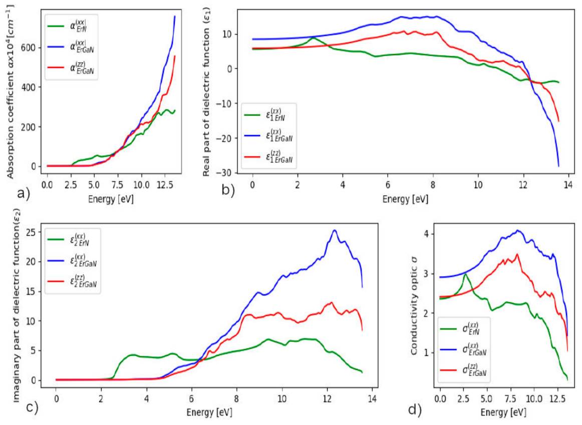
Figure 6 Optical properties: a) absorption coefficient, b) Real part(ϵ1), c) Imaginary part (ϵ2) of dielectric functions and d) optical conductivity (σoc) of ErN and Er0.125Ga0.875N materials. 

Figure 7 Index refraction and extinction coefficient of ErN and Er0.125Ga0.875N materials. 

3.3 Transport properties

The effectiveness of a material for TE applications is determined by the dimensionless figure of merit, ZT=σS2T/κ, where S is the Seebeck coefficient, σ is the electrical conductivity, T is the absolute temperature, and κ is the thermal conductivity. High values of figure of merit require high values of S and σ and low value of κ. The power factor of a TE material is given by P=σS2, which involves all the important electrical properties of the material. Our calculations of TE for ErGaN/ErN are performed separately on bulk materials, using the BoltzTrap code [21].

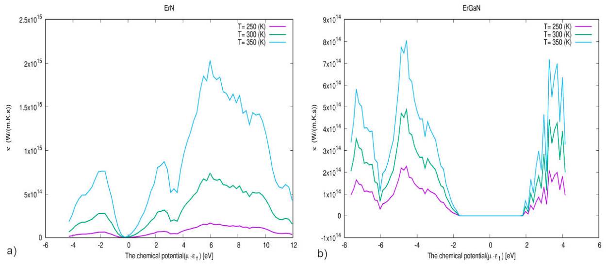
The electrical conductivity as a function of chemical potential at three constant temperatures (250,300,350) K is shown in Fig. 8, where it is clear that (σ/τ) of ErN and ErGaN increases as temperature decreases. The maximum electrical conductivity (σ/τ) of ErN and ErGaN was found to be 6.2 ×10211/Ωms and 3.7 × 10201/Ωms at 5.3 eV and 3.5 eV, respectively, at 250 K. The electronic thermal conductivity (κ) as a function of chemical potential is plotted in Fig. 9, and it shows clearly that κ for ErN and ErGaN increases as temperature rises. The Seebeck coefficient as a function of chemical potential at (250,300,350)K is shown in Fig. 10. Its maximum values were found to be 530 μV/K (at 250 K) and 1400 μV/K (at 300 K) respectively. In Fig. 11 shows the electronic power factor (PF) calculated as a function of chemical potential at three constant temperatures. Our calculated show that ErN has its the highest power factor with a value of 6 × 10⁹ W/mK 2s at 350 K and energy level of ErN is 9 × 10¹⁰ W/mK2s at 350 K and energy level of 2 eV. The electronic power factor is a keynote quantity for measuring transport properties.

Figure 8 Electrical conductivity of ErN and Er0.125Ga0.875N at three constant temperatures. 

Figure 9 Electronic thermal conductivity of ErN and Er0.125Ga0.875N at three constant temperatures. 

4 Conclusion

We have studied materials involved in constructing QW of Er0.125Ga0.875N/ErN by ab-initio calculation using DFT theory. The obtained results of the electronic properties show clearly ErN to be a semiconductor with an indirect band gap at 0.79 eV and that Er0.125Ga0.875N presents an indirect band gap at 3.38 eV, using GGA+U approaches, which is in good agreement with other calculations. This indirect band gap was found to improve carrier extractions and lead to improved performance of these properties. The real and imaginary parts of the dielectric function and the optical coefficients were determined. Transport properties of Er0.125Ga0.875N and ErN have been investigated by employing the Boltzman theory implemented in the BoltzTrap code, the electrical conductivity, Seebek coefficient, electronic thermal conductivity, and electronic power factor have been determined; their values show that these materials could be potential candidates for energy conversion. The quantized energy levels present in a quantum well, which can be tuned, provide an opportunity to increase the limited efficiency of solar cells.

References

[1] L. C. Bannow et al., An ab initio based approach to optical properties of semiconductor heterostructures, Model. Simul. Mater. Sci. Eng. 25 (2017) 065001, https://doi.org/10.1088/1361-651X/aa7478. [ Links ]

[2] R. Dahal, C. Ugolini, J. Y. Lin, H. X. Jiang, and J. M. Zavada, Erbiumdoped GaN optical amplifiers operating at 1.54 μm, Appl. Phys. Lett. 95 (2009) 111109, https://doi.org/10.1063/1.3224203. [ Links ]

[3] S. Tab et al., Structural, elastic, electronic, and magnetic properties of quaternary alloys BBi0.75 Mn0.125 N0.125: A first-principles study, Rev. Mex. Fis. 66 (2020) 627, https://doi.org/10.31349/RevMexFis.66.627. [ Links ]

[4] B. Amiri, A. Lazreg, and F. A. Bensamer, Optical and Thermoelectric properties of Gd doped Wurtzite GaN, Optik 240 (2021) 166798, https://doi.org/10.1016/j.ijleo.2021.166798. [ Links ]

[5] A. G. Petukhov, W. R. L. Lambrecht, and B. Segall, Electronic structure of rar-earth pnictides, Phys. Rev. B 53 (1996) 4324, https://doi.org/10.1103/PhysRevB.53.4324. [ Links ]

[6] K. P. O’Donnell and V. Dierolf, Rare Earth Doped III-Nitrides for Optoelectronic and Spintronic Applications (Springer, Dordrecht, 2010), https://doi.org/10.1007/978-90-481-2877-8. [ Links ]

[7] C. Ugolini et al., Formation energy of optically active Er3+ centers in Er doped GaN, Appl. Phys. Lett. 101 (2012) 051114, https://doi.org/10.1063/1.4742196. [ Links ]

[8] S. Kasap and P. Capper, Nano-Engineered Tunable Photonic Crystals, in Springer Handbook of Electronic and Photonic Materials (Springer, Cham, 2017), https://doi.org/10.1007/978-3-319-48933-9. [ Links ]

[9] T. Trupke, M. A. Green, and P. Würfel, Improving solar cell efficiencies by up-conversion of sub-band-gap light, J. Appl. Phys. 92 (2002) 4117, https://doi.org/10.1063/1.1505677. [ Links ]

[10] M. Haase and H. Schäfer, Upconverting Nanoparticles, Angew. Chem. Int. Ed. 50 (2011) 5808, https://doi.org/10.1002/anie.201005159. [ Links ]

[11] M. B. Spitzer, H. P. Jenssen, A. Cassanho, An approach to downconversion solar cells, Sol. Energy Mater. Sol. Cells 108 (2013) 241, https://doi.org/10.1016/j.solmat.2012.08.011. [ Links ]

[12] A. J. Steckl, J. H. Park, andJ. M. Zavada , Prospects for rare earth doped GaN lasers on Si, Mater. Today 10 (2007) 20, https://doi.org/10.1016/S1369- 7021(07)70176-1. [ Links ]

[13] T. M. Al Tahtamouni, M. Stachowicz, J. Li, J. Y. Lin , and H. X. Jiang , Dramatic enhancement of 1.54 μm emission in Er doped GaN quantum well structures, Appl. Phys. Lett. 106 (2015) 121106, https://doi.org/10.1063/1.4916393. [ Links ]

[14] W. Kohn, Density Functional and Density Matrix Method Scaling Linearly with the Number of Atoms, Phys. Rev. Lett. 76 (1996) 3168, https://doi.org/10.1103/PhysRevLett.76.3168. [ Links ]

[15] W. Kohn and L. J. Sham, Self-Consistent Equations Including Exchange and Correlation Effects, Phys. Rev. 140 (1965) A1133, https://doi.org/10.1103/PhysRev.140.A1133. [ Links ]

[16] P. Blaha et al., WIEN2k: An Augmented Plane Wave Plus Local Orbitals Program for Calculating Crystal Properties, 2001. [ Links ]

[17] E. Sjöstedt, L. Nordström, and D. J. Singh, An alternative way of linearizing the augmented plane-wave method, Solid State Commun. 114 (2000) 15, https://doi.org/10.1016/S0038-1098(99)00577-3. [ Links ]

[18] K. Schwarz and P. Blaha, Solid state calculations using WIEN2k, Comput. Mater. Sci. 28 (2003) 259, https://doi.org/10.1016/S0927-0256(03)00112-5. [ Links ]

[19] B. N. Harmon, V. P. Antropov, A. I. Liechtenstein, I. V. Solovyev, and V. I. Anisimov, Calculation of magneto-optical properties for 4f systems: LSDA + Hubbard U results, J. Phys. Chem. Solids 56 (1995) 1521, https://doi.org/10.1016/0022-3697(95)00122-0. [ Links ]

[20] F. Tran and P. Blaha, Accurate Band Gaps of Semiconductors and Insulators with a Semilocal Exchange-Correlation Potential, Phys. Rev. Lett. 102 (2009) 226401, https://doi.org/10.1103/PhysRevLett.102.226401. [ Links ]

[21] G. K. H. Madsen, J. Carrete, and M. J. Verstraete, BoltzTraP2, a program for interpolating band structures and calculating semi-classical transport coefficients, Comput. Phys. Commun. 231 (2018) 140, https://doi.org/10.1016/j.cpc.2018.05.010. [ Links ]

[22] J.-S. Filhol, R. Jones, M. J. Shaw, and P. R. Briddon, Structure and electrical activity of rare-earth dopants in GaN, Appl. Phys. Lett. 84 (2004) 2841, https://doi.org/10.1063/1.1710710. [ Links ]

[23] M. Lantri et al., Effect of Erbium doping on GaN electronic and optical properties: First-principles study, Mod. Phys. Lett. B 33 (2019) 1950327, https://doi.org/10.1142/S0217984919503275. [ Links ]

[24] A. Lazreg , Z. Dridi, F. Benkabou, and B. Bouhafs, Electronic structure of cubic ErxGa 1-x N using the LSDA+U approach, Phys. B 403 (2008) 2702, https://doi.org/10.1016/j.physb.2008.02.003. [ Links ]

[25] P. Larson, W. R. L. Lambrecht, A. Chantis, and M. van Schilfgaarde, Electronic structure of rare-earth nitrides using the LSDA+U approach: Importance of allowing 4f orbitals to break the cubic crystal symmetry, Phys. Rev. B 75 (2007) 045114, https://doi.org/10.1103/PhysRevB.75.045114 [ Links ]

[26] J. Singh, Optical Properties of Condensed Matter and Applications (John Wiley and Sons, New York, 2006), https://doi.org/10.1002/0470021942. [ Links ]

[27] B. Amiri , A. Belghachi, H. Benslimane, and A. Talhi, Potential of multiplequantum well tandem solar cells based on GaPxAs 1-x /GayIn 1-y As, Optik 147 (2017) 283, https://doi.org/10.1016/j.ijleo.2017.08.081. [ Links ]

[28] S. Fara, P. Sterian, L. Fara, M. Iancu, and A. Sterian, New Results in Optical Modelling of Quantum Well Solar Cells, Int. J. Photoenergy 2012 (2012) 810801, https://doi.org/10.1155/2012/810801. [ Links ]

[29] P. Harrison and A. Valavanis, Quantum Wells, Wires and Dots: Theoretical and Computational Physics of Semiconductor Nanostructures, 4th ed. (Wiley, New York, 2016). [ Links ]

Received: May 15, 2021; Accepted: August 30, 2021

Creative Commons License This is an open-access article distributed under the terms of the Creative Commons Attribution License