


 text new page (beta)
 English (pdf)
 Article in xml format
 Article references
 Send this article by e-mail
 Cited by SciELO
  Similars in
SciELO
Similars in
SciELO 
 Permalink
1. Introduction and outline
It should not be a controversial undertaking to change the dimensionality of a physical system. On the one hand and when things go well, it leads to suggestive new viewpoints. On the other hand, new polemics and paradoxes arise. In the classic book “A Brief History of Time”, Stephen Hawkings wrote on the impossibility of two-dimensional (2D) life-forms by showing that digestion will be next to impossible. Yet, there are recent claims that 2D worlds are not necessarily “too simple” for life to exist [1]. If Phil Anderson’s manifesto “More Is Different” brings out the importance of having more elements to increase the complexity and have new emerging laws [2], the discovery of 2D materials showed the other side of the coin [3]: less is also different. And when looking at its physical properties, 2D materials can result in a quite different manifesto: sometimes less is more.
More amazing electronic, optical, and mechanical properties, like the material with the highest known electrical and thermal conductivity, highest known electronic moblility, and elasticity [4], yet many of these 2D materials can be strained, bent, and wrinkled as a soft material [5]. The 2D materials revolution started with graphene, a one-atom layer of carbon extracted from graphite [3,6]. A 2D crystal was thought to be impossible to make, as according to the Mermin-Wigner theorem there is no order with short-range interactions at a temperature different from zero. Eventually, it turns out that such theorem was literally too rigid to be applied in a realworld situation; graphene is a 2D membrane that lives in a 3D world, and it vibrates like a drum pad. Such vibrations, known as flexural modes, allow 2D materials to evade the fate predicted by many eminent theoretical physicists. In a record time of 6 years from graphene’s discovery, A. Geim and K. Novoselov were awarded the 2010 Nobel prize. As a lesson, this shows that still in the XXI century, there is a place for simple tools as adhesive tape, graphite, and an optical microscope if good ideas, creativity, and hard work is present. A second Nobel prize was given in 2016 to D.J. Thouless, F.D.M. Haldane and M. Kosterlitz for another 2D related discovery: topological phase transitions and topological phases of matter. This work was made nearly 40 years before the graphene’s discovery but pointed out in the same direction: order is not impossible in D< 3 at finite temperature, it is just a bit different.
Since the discovery of graphene, the main feature of any 2D material is now clear: what makes them special is their all surface nature. This leads to novel paths in physics as interactions are maximized. Afterward, new 2D materials were discovered, and now they are classified in families [7,8]. A short-list of these main 2D families is the following,
Almost flat structures. Graphene is the most representative case. Other examples are Silicene, Germanene, hexagonal Boron Nitrate (h-BN), Borophene, Stanene. Most of the early research was made in this area.
Puckered structures that are not completely flat. The most famous examples are transition metal dichalcogenides (TMDs) with a general formula MX2, with M a transition metal (Mo, W, Ti, Nb, etc.). Atom X can be a chalcogen element (Se, S, or Te), or group III-VI or IV-VI elements, producing materials as InSe, GaSe, GeSe, SnSe, SnS2, SnSe2.
2D transition metal carbides and nitrides, also known as MXenes. Their general formula is Mn+1Xn. Here M represents a transition metal, and X represents C or N (where n is 1, 2, or 3) with a surface terminated by O, OH, or F atoms.
The other three families are in the process of being investigated, 2D oxides and hydroxides, group-IV monochalcogenides (MX with M = Ge, Sn, and X = S, Se, Te), and 2D organic materials as pentacene or α − T 3 graphene. From there, one can stack layers to form heterostructures as Moiré patterns [9], twisted bilayer and trilayer graphene [1’], etc. At this moment, there is a lot of research in this area due to the recent discovery of superconducting phases [11]. This results in a quantum phase diagram akin to those seen in highTc superconductors [1’-12]. An important area is the study of how strain affects the electronic and optical [7,8,13-17]. The reason is twofold. On the one hand, the substrates induce lattice deformations, and on the other hand, the control of strain allows to modify the characteristics of a material. This results in a field known as straintonics. Similarly, there are other ways to control the optical and electronic properties: twistronics [11], valleytronics [18], origami and kirigami, and spintronics [19].
An important feature of 2D materials is the use of relativistic quantum equations as the Dirac and Weyl equations [20]. Moreover, strain can be included as pseudo magnetic fields with the notable property of producing fields much higher than real ones [20]. As expected, the marriage of solid-state physics with high energy approach has been very fruitful as allowed to produce in the lab effects that were impossible to be seen in otherwise much experimentally demanding systems [21]. We can cite the Klein effect [20], effects of the Dirac equation in curved spaces [22], and even analogies to black holes [23].
As expected, many reviews and books are covering all these topics [24,25]. Now the question is why to make another one. There are many answers to this question. The first is that the present review is focused on developing the tools to understand heterostructures and, from there, allow the reader to dig into complex quantum phase diagrams. It also covers topological properties and time-dependent topological properties. Also, we try to focus on questions that our group in Mexico pursued systematically, even a few months after the discovery of graphene in 2004; for example, why do Dirac cones appear, a question that the reader will probably not find in other reviews as somehow is bypassed as a legitimate question and eclipsed by the mathematics. Other questions posed during such period with Ph. D. students at the Instituto de Física, UNAM were the effects of the disorder, electromagnetic radiation and time-dependent strain without using perturbative methods, a subject that now is mainstream but was starting at that moment. After many years we developed tools and results that have been proved to be useful in the study of other 2D materials. And more importantly, in this review, we stick with the idea that most of the complex properties are contained in simple models that give a lot of insights into physics, and eventually give a physical sense to mathematics. In particular, here we include our new results on producing the simplest hamiltonian that describes twisted graphene at magic angles, bringing to the forefront its topological nature and the three main physical driving forces: quantum confinement, frustration balance and non-Abelian gauge fields.
The layout of this work is as follows. We start with a section devoted to defining the structure and diffraction properties. Then we study Dirac materials and their variants, multilayered 2D materials, and finally, we discuss superlattice properties.
2. Structure and diffraction of 2D materials
Compared with its 3D counterparts, the study of 2D materials structure and diffraction may seem to be simple, but in fact, it has its particularities and difficulties. If we stick with family one of our list, i.e., almost flat structures, we describe its structure using the point lattice,
where a1 ,2 are the Bravais unitary vectors (see Fig. 1) and n 1 ,n 2 integers. The most simple case is graphene, in which the point lattice is given by a trigonal one that we will call A sublattice with vectors,
where a = 1.42 Å is the distance between C atoms [26].˚ Also, we need to add a basis vector b j that points to the different atoms of the unit cell; in other words, it describes the so-called decoration of the unit cell. In graphene, if C atoms are at sites r n1 ,n 2, the others are made by a simple translation δ1 of these points, forming the B sublattice. As seen in Fig. 1, the lattice turns out to be a honeycomb one. For further reference, it is useful to define the vectors,
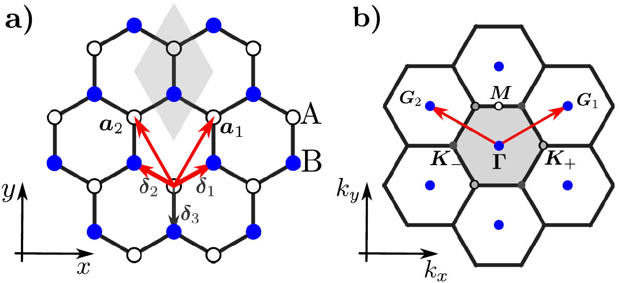
FIGURE 1 a) Graphene honeycomb lattice showing the unit cell (shaded), the Bravais vectors a 1 and a 2, which define a trigonal lattice. The first-neighbor vectors δ1, δ2, and δ3 are also indicated. The bipartite sublattices A and B, which define two trigonal lattices, are shown. b) First Brillouin zone (shaded) of graphene and the high-symmetry points K+ and K−. The Fermi level and the Dirac points coincide withthe inequivalent high symmetry points K+ and K−
The vectors δ2 and δ3 can be written using the basis and Bravais lattice vectors,
An important property is that A sublattice atoms only have as neighbors B lattice atoms and viceversa. Such lattices are called bipartite and are fundamental as they give an extra symmetry that proves relevant in all of its properties. Figure 1b) presents the reciprocal lattice vectors:
and the first Brillouin zone (1BZ). Two high-symmetry points
The diffraction can be obtained from the form and atomic structure factors. A simple example is to consider Dirac delta-function scatterers centered at each lattice site:
where r l are the atom positions. The diffraction pattern is given by the norm of the Fourier transform of V (r),
As an example, we consider a decorated version of the honeycomb lattice as in h-BN. Here the A sublattice can be occupied by Nitrogen atoms while the other sublattice is occupied by Boron atoms. These atoms each have a scattering potential V 0 and V 1, from where
As seen in Fig. 2, the diffraction is made from spots at the trigonal lattice reciprocal vectors. A spot in location lG1 + hG2 has intensity,
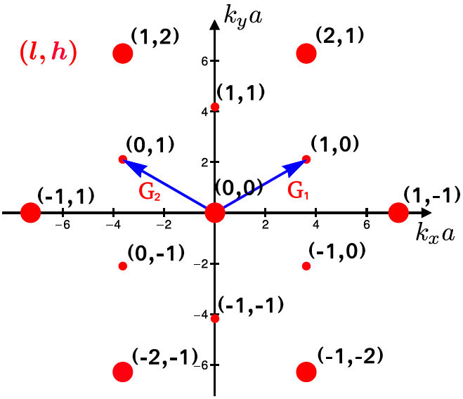
FIGURE 2 A typical diffraction pattern for a 2D materials, in this case graphene. The Miller indexes l and h label each diffraction spot position and the amplitude is given by F(l,h).
where l,h are the Miller indexes. If we now make the atoms the same as in graphene V 0 = V 1, we recover graphene’s case,
with two possible intensities
Strain and flexural deformations. The recipe is to add a strain vectorial field au(r).
Stacking of multiple layers. Diffraction is just the sum of each layer diffraction.
The strain and flexural deformation field can be periodic, random, or quasiperiodic and has been studied in a previous review [29]. For periodic strain, satellites peaks appear close to the Bragg lines, while for disordered cases, the spots broaden. Also, the Brillouin zone can be folded back as seen in Kekule bond patterns [18,30].´
In the multilayered case, with rotated layers and if we suppose that the lattices are not deformed, the diffraction pattern is a superposition of the rotated reciprocal lattices corresponding to each layer [9]. Rotations and displacements lead to different space groups [31] (known in 2D as wallpaper groups). A very powerful method, originally developed to treat quasicrystals, allows describing the lattice positions and diffraction using higher-dimensional lattices, even providing extra information as the coincidence lattice, which determines many physical properties of heterostructures [32].
3. Electronic properties of Dirac materials
The experimental values of the electronic properties of graphene and other 2D materials have been extensively discussed in several reviews [20,25]. Here we only made few useful remarks. In particular, what matters for the electronic and optical properties are the most energetic electrons, i.e., those with energies within a band of width k B T (being T the temperature and k B the Boltzmann constant) around the Fermi energy (E F ). Their velocity, concentration, and mean free path will control such properties.
Although in graphene’s we use relativistic quantum mechanics to describe electrons, in reality, the Fermi velocity v F is around c ≈ v F /300 with c the speed of light, which is by no means unusual and is comparable to other 3D material, as for example, Silicium. Moreover, as we will see below, the charge density is very low. This points out to the most two remarkable properties of graphene, the large mean free path even at room temperatures due to the absence of backscattering [24] and the possibility of changing the carrier concentration by electric doping. In other words, while semiconductors are doped chemically with p or n donors, in graphene, such doping is tuned dynamically by an external field to generate holes or electrons. This property has not been fully used in electronic devices, but it stands out as unique.
The electronic properties of graphene are surprisingly well described by a one-band tight-binding Hamiltonian [26,33]. As what matters is the Fermi level, a low-energy approach leading to an effective Dirac Hamiltonian turns out to be very useful. As we will see, this idea permeates to other 2D materials. Below we present a minimal approach to these models.
3.1. Dirac materials: graphene
Carbon has four electrons in valence orbitals, but three of them are used to make in-plane sp 2 covalent bonds with its three neighbors [34]. The remaining electron half-fills each Carbon π− hybrid orbital [34]. Neglecting the three valence electrons as their energetic contributions are far from the Fermi level, this leads to a one-band tight-binding (TB) Hamiltonian [26]:
where r
j
indicates atoms in the A sites positions. The hopping or transfer integral is t
0 ≈ 2.7 eV by fitting experimental data [26].
where k is a wavevector, and a similar transformation holds for br+δ n , resulting in,
The leads to an effective 2 × 2 Hamiltonian H(k). The Schrödinger equation is now,
where H AB (k) = −t 0 f(k), and f(k) is a complex function:
The energy dispersion is readily found from the eigenvalues of Eq. (14):
For a system with N sites, the eigenfunctions in real space are,
Figure 3 presents the surface E(k) obtained from Eq. (17). First, notice the symmetry around E = 0, known as the particle-hole symmetry. This is a consequence of the bipartite property and can be understood from the CyrotLackmann theorem as a result of the absence of odd-rings in the lattice [40]. Without charge doping by external fields, the π orbitals are half-filled, and therefore, the Fermi energy (E
F
) lies at E = 0. As indicated in Fig. 3, Eq. (17) displays a conical dispersion near E = 0. The condition E = 0 produces two special points labeled by K
D
, known as Dirac points. For pristine graphene, K
D
coincides with K±. For strained graphene, these points do not coincide, and there have been many confusions in the literature about this point [14,16]. The existence of two inequivalent Dirac points leads to the concept of the valley to classify the regions around each cone tip [26]. Let us see how Equation (17) produces cones: for a crystal momentum k = K
D
+ q with
where v F is the Fermi velocity:
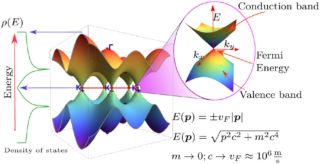
FIGURE 3 Energy dispersion obtained from Eq. (17). To the left, we show its corresponding DOS (ρ(E)). A zoom-in at the Fermi energy showing a cone is displayed as well. The vertices of the cones touch at the Dirac point, here at the high-symmetry points K± with linear dispersion. The Fermi energy is at E = 0. At the Dirac cones, the DOS behave as ρ(E) ∼ E, while the saddle points of Eq. (17) produce the Van Hove singularities, which are the two peaks in the DOS. They correspond to highly degenerated dimer states and signal the energy where frustration plays a role, therefore depleting the DOS and producing the Dirac cone.
This leads to a linear DOS:
and to the following carrier density:
Dirac cones are disorder protected by topology [41]. Graphene nanoribbons are studied using similar techniques leading to gaps that depend upon the width allowing to design electronic devices [42].
3.1.1. Rise of Dirac cones as a frustration effect in triangular lattices
An important and legitimate question is, after all, why do physically Dirac cones appear. Not many people ask this important question, so here we discuss how this is a consequence of the bipartite nature of the lattice and, more importantly, to the wavefunction frustration due to the triangular symmetry [38,43]. To see this, consider the squared Hamiltonian obtained from Eq. (13):
Now the wave function components on the A and B sublattices are decoupled. Therefore H 2 0 describes a triangular lattice as it removes one bipartite sublattice [38,43]. As illustrated in Fig. 4, the spectrum of H 2 0 is obtained by folding around E = 0 the H 0 spectrum.
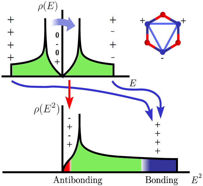
FIGURE 4 Sketch of the Hamiltonian eigenvalue renormalization from a graphene hexagonal lattice into a triangular one by the transformation H 2: the graphene’s density of states ρ(E) is transformed into ρ(E 2), resulting in a folding around E = 0 that is indicated by arrows. Band edges, central states, and phase differences among sites are represented by ± signs. Central states at E = 0 have a zero amplitude in one sublattice [37]. When one of the sublattices is renormalized, states near E = 0 result in edge band states with an antibonding nature in a triangular lattice [38,43], as indicated in the triangle that appears inside the hexagon. Due to frustration, states are pushed to higher energies, leading to van Hove’s degeneracies seen as peaks.
The eigenstates of H 0 at E = 0 have zero amplitude in one bipartite lattice (see Fig. 4]. A state with E = 0 is a ground state of H 2 0. Nearby states have an antibonding nature in the sense phases differences are maximal for neighbors. We can see this by writing Eq. (17) without any reference to the first neighbor vectors δ n by using Eq. (4),
Equation (24) gives the energy in terms of one of the triangular sublattice amplitudes and phases. The cosine terms in Eq. (24) give the bond contribution due to triangles while the first term is the self-energy of H 2 0, which is always the local coordination [40], in this case, Z = 3.
The ground state of Eq. (24) can be estimated from a variational procedure by considering a wave function with a maximal phase difference to decrease frustration, such as,
from where
While in Eq. (24), the first two cosine terms will give each a contribution −2t 0, the third cosine increases the energy by 2t 0, and is thus frustrated, as shown in Fig. 4. This results in E(k) = ±t 0, which coincides with the Van Hove singularities of graphene. They are made from localized uncoupled dimers, disconnected from the lattice by having neighbors with zero amplitude. The degeneracy is given by the number of dimers, which is always N/2.
To further reduce the energy below E 2 = 1, the frustration needs also to be reduced. To see this, again, we use a variational wave function by proposing in Eq. (24) the following phases,
where ϕ = 2π/3, and finally we obtain E(k)2 = 0. It turns out that this special wavevector is precisely the point k = K+. We get the other Dirac point k = K− by choosing the other possible combination of phases. As for E = 0, the states are pseudo-spin polarized, the minimal frustrated state is four-fold degenerated. Then, as the energy goes from E 2 = t 2 0 to E 2 = 0, the DOS goes from a massive degenerated state to a four-fold degenerated state. For disordered systems, the probability of finding regions without frustration decreases exponentially, and a Lifshitz tail appears. In graphene, it leads to the Dirac cone where the DOS goes linearly to zero towards E → 0. Once graphene’s periodicity is broken by impurities or edges, confined zero-energy modes appear.
These E = 0 flat-band modes appear due to disorder or boundaries and are associated with topological properties [37,40]. Zero-energy modes are strictly localized and confined [40,44]. For doped graphene, the number of zeroenergy modes is obtained by summing disordered configurations [37]. Such flat bands are especially prominent at graphene on top of twisted graphene, inducing superconductivity [11]. The Lifshitz tail produces a pseudo mobility edge near the Dirac cones [43,45], as confirmed in ARPES experiments [46]. Resonant states are seen near the Fermi energy [45,47,48], and the wavefunctions are multifractal [38].
To further quantify the frustration, especially for the continuous models, notice how the electron dispersion depends only on the phase difference between neighboring bonds. Using Eq. (18), this suggests defining a function to measure frustration,
where the label δ1 was dropped in b ∗ k(r j + δ1) as on to each site in A, we assign only one neighbor site B. The minus sign is now irrelevant in the squared Hamiltonian. Now we sum all bonds contributions and observe that,
In the previous expression, a
s
denotes second neighbors in H
0, which are first-neighbors in
where the bonding (frustration) plus antibonding contributions are,
The ground state E = 0 is obtained when the frustration and antibonding contributions balance the self-energy in such a way that F(K±) = −3. The frustration increases as the momentum depart from the K± points.
3.1.2. Low-energy approximation: Dirac equation
As what matters most is electrons around the Fermi energy, it is very useful to find an effective hamiltonian by considering k = K± + q. The expansion of the hamiltonian Eq. (14) up to first order in q and around K+ is [50,51]:
where σ = (σ x ,σ y ) are Pauli matrices. The momentum is p = ℏq. A similar expansion can be made around K − to give,
with σ∗ = (σ x ,−σ y ). Now replace q → −i ℏ ∇ in correspondence to the k · p approximation. The hamiltonians (32) and (33) are two-dimensional Dirac-like hamiltonian for massless fermions [52]. Notice that we used the word Diraclike as in a strict sense, there is no Dirac equation in; despite this, most people refer to this 2D version as the Dirac hamiltonian. The description given so far was in terms of Pauli matrices. They operate on spinors that here describe the wave function on each sublattice instead of a real spin. The term pseudospin is thus used to call this sublattice degree of freedom. In fact, before we kept both valleys separately, but the full structure of the hamiltonian taken into account both valleys is,
where Π = ℏ (p x +ip y ), and H operates into a bispinor wavefunction. Their components now describe pseudospin and valley,
The full hamiltonian structure is sketched out in Fig. 5. One interesting property is chirality. To see this, write Eq. (32) and Eq. (33) as,
where
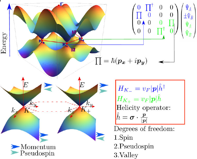
FIGURE 5 Energy dispersion obtained from Eq. (17) considering all degrees of freedom: spin, pseudo spin, and valley. The arrows indicate the direction of the pseudospin along the with momentum on each Dirac cone and each band. For a given Dirac cone, the helicity is inverted on each band.
It represents the projection of pseudospin on the momentum, and as
and the valley helicity (chirality) operator is
The index ζ = 1 indicates valley K + and ζ = −1 valley K−. ζ is known as the valley degree of freedom. The helicity operator has eigenvalues h 1 = 1 and h −1 = −1 with eigenvectors,
Figure 5 presents a short summary of how the pseudospin, band, and valley are related to each other in the band structure.
3.2. Measuring frustration in continuous models
Let us show how frustration ideas translate into continuous low-energy models [53]. Consider first the Dirac low-energy model. To evaluate frustration, we look for the least frustrated state, which occurs for K±. Then we expand F(k+) using k = K+ + q where qa 0 ≪ 1,
The Fermi velocity can be thus interpreted as the rate of frustration growth with q. For other 2D materials, it is useful to introduce a technique to measure frustration in such a way that although the energy dispersion may not be known, the ground state is reachable by using a variational procedure [53].
The method relies on noticing that still for continuous models, the phases between neighbors are given by the components of the spinor, and it follows that
where Z 2 is the number of neighbors and the integral is made in the unitary cell. The ground state is thus the one with ∇g k(r) = 0.
3.2.1. Graphene’s nearly free electron bands: charge images near a conducting plane
While many of graphene’s electronic properties are extremely well described by the Dirac approach or the TB approximation, it turns out that not all properties are well described under such approximations. Figure 6 presents a numerical calculation of graphene’s bands showing parabolic nearlyfree electron bands 3 eV above the Fermi energy [54-57]. The explanation of why this happens comes from a simple physical mechanism. If we think of graphene as a conducting plane, electronic clouds outside the plane will induce image charges [54,58-60]. When graphene interacts with substrates, adatoms, free molecules, etc., such states are important. As an example, graphene can become metallic with water, as the dipolar water layer lowers the nearly-free electron charge until it touches the Fermi energy [61]. This mechanism is akin to the flat band seen in twisted graphene bilayers, and we believe that such mechanism is in play for superconductivity in doped graphene laminates [61-64]. Further evidence is provided by recent reports of high-temperature superconductivity for water-treated graphite [65,66]. By using a simple model of an electron interacting with its charged image, a model akin to an effective Hydrogen atom is found [59]. The energy dispersion is,
here k|| is the wave-vector parallel to the graphene plane, m ∗ is the effective mass.
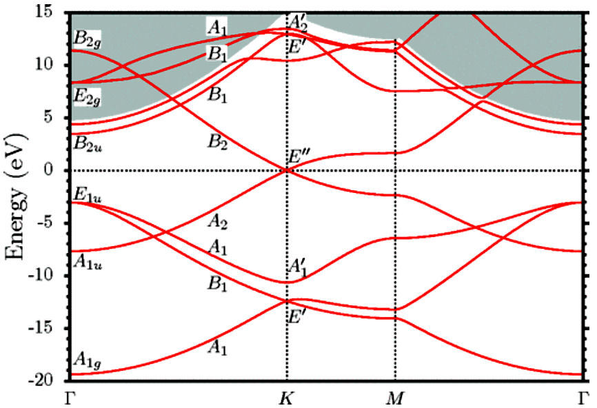
FIGURE 6 Graphene bands evaluated numerically using the full potential linearized plane wave method (FP-LAPW) and the localdensity approximation (LDA). The lines are single graphene bands, while the gray background corresponds to the continuous spectrum. Each band is classified according to the symmetry group representations. The nearly parabolic free-electron bands are indicated with labels B 2u . Their shape is well approximated by Eq. (43) and Eq. (44) using n = 0 and n = 1. Reprinted figure with permission from Ref. [55]. Copyright (2012) by the American Physical Society.
E n is found by solving the Schrödinger equation of an electron attracted by its image charge [67]. This leads to the Rydberg like series of states seen in Fig. 6. To better treat the regions close to the plane, LDA calculations are needed and matched with the analytical solutions, resulting in [54,58],
where a 2 is the matching distance of the analytical and numeric solution. This Rydberg series has been confirmed by photon photoemission spectroscopy [68]. A very important warning is in play here because the long tail of the image charge Coulomb potential is not well described in DFT calculations [60], a point ignored by many workers who model interactions of graphene with other materials.
3.2.2. Disorder effects
The coupling of the valley and pseudospin degrees of freedom is important in charge transport. As seen in Fig. 5, conduction electrons near a given valley, say the K− valley, have momenta anti-parallel to the pseudospin. For back-scattering to occur, the momenta need to be reversed, i.e, to change from p to −p. This requires to invert the pseudospin and therefore valley, but valleys are far away in momentum, so backscattering is not possible, explaining the graphene’s long coherence lengths [24].
Disorder effects are understood through the study of the Dirac equation and the induced broken symmetries [69,70]. Despite this, the Dirac equation does not capture all effects of the disorder. Vacancies and impurities with enough selfenergy can produce backscattering [43,46]. Based on the frustration picture, a quasi-mobility edge was predicted in doped graphene [43] and was experimentally confirmed [46]. This topic is still controversial, as according to the orthodox theory, no mobility edges are seen in 2D systems. However, graphene has many symmetries, and disorder induces multifractal power-law localized states [37], for which the general theory used may not be valid.
3.2.3. Electromagnetic, strain and flexural fields
To understand the interaction of 2D materials with electromagnetic fields, there are two paths. One is to use perturbation techniques in which the field does not induce changes in the band structure. The first approach allows to calculate the transmittance, optical, and ac electrical conductivity for weak fields [19,71]. One can also include secondnearest-neighbors in the optical conductivity calculations using the non-equilibrium Green’s function formalism [72]. For graphene, the transmittance is almost frequency independent.
Here we do not follow these paths are they can be found elsewhere [71,72]. Instead, we focus on using a Floquet approach that fully includes the space-time periodicity of the external field and material [73,74].
Also, related to this topic, we add that strain and flexural deformations enter as a pseudo-electromagnetic field in the Dirac equation, and therefore, many results found for the electromagnetic theory can be applied to strain fields [20]. Despite its similarities, a real electromagnetic field breaks the time-reversal symmetry while a pseudo electromagnetic field does not. From a formal point of view, this only changes some signs on each valley; however, the resulting currents induced by the pseudo fields on each valley are canceled out. This not happens for electromagnetic fields, as the currents have the same sign on each valley [73,74].
We remark here that in 2013 we showed that the basic equations used in the continuous low-energy Dirac approximation had a problem as they were not able to solve even the simplest case, an isotropic uniform expansion [14]. The reason was found in Ref. [14]; when making the low-energy approximation in the tight-binding problem, one needs first find the Dirac points and then perform the approximation, as strain moves the Dirac points. Other groups done the approximation in the inverse order, and thus many results were wrong. This problem was fixed in Ref. [14] by producing the proper form of the hamiltonian for uniform strain. From there, a solution for general strain fields was constructed [16].
The analogy between strain and electromagnetic fields is very useful; for example, one can find solutions for Dirac fermions in magnetic fields [75] and translate them to strain. Strain leads to many effects, for example, a light-induced Faraday effect [76], tunable dichroism [17,77]. Moreover, strain and real magnetic fields can be combined to build new kinds of devices; for example, there is a theory that proposed quantum engine based on the gauge fields formalism [78] or valley-polarization of currents by nanobubbles [79].
We started in 2007 working in non-perturbative methods for electromagnetic waves [73,74]. Afterward, some results were extended for deformations. For example, ripples in graphene can be studied by using the minimal coupling in the Dirac hamiltonian as if it were an electromagnetic field, [73,74,80],
where η = ±1 labels the K + and K + Dirac points. A and V are pseudo-vector and pseudo-scalar potentials [20],
where the strain is characterized by the 2×2 tensor ε
µν
with components µ = x,y and ν = x,y, defined below. The dimensionless Grüneisen coefficient
The out-of plane deformation is,
with a phase of the wave given by,
h(r,t) measures the deformation with respect to the normal of flat graphene and Q is the deformation wave vector with components (Q 1 ,Q 2). The time-frequency of the strain is given by Ω, which is related with Q = |Q| as Ω/Q = v s , where v s is the deformation propagation velocity, usually the velocity of sound. Then in-plane strain can be written is a similar way,
The electron dynamics is now dictated by the equation,
The method to find its solution is the same that we used to solve the analogous of Eq. (52) for electromagnetic fields [73,74]. The idea is to combine a Floquet theory with a Volkov approach, i.e., the solution is made from a plane wave and a function that depends only on the phase of the field. This is equivalent to solve the Dirac equation in the reference frame of the wave [73,74],
where Φ ρ (ϕ) is a function to be determined for each sublattice ρ = A,B, and E = v F ~|k|. This ansatz transforms the partial differential equations (52) into an ordinary secondorder differential equation. In all cases that we studied, the resulting effective equation turned out to be a Mathieu equation that describes a classical parametric pendulum [73,80]. Here we offer a simplified version for the case of an electron with momentum parallel to the wave propagation,
where
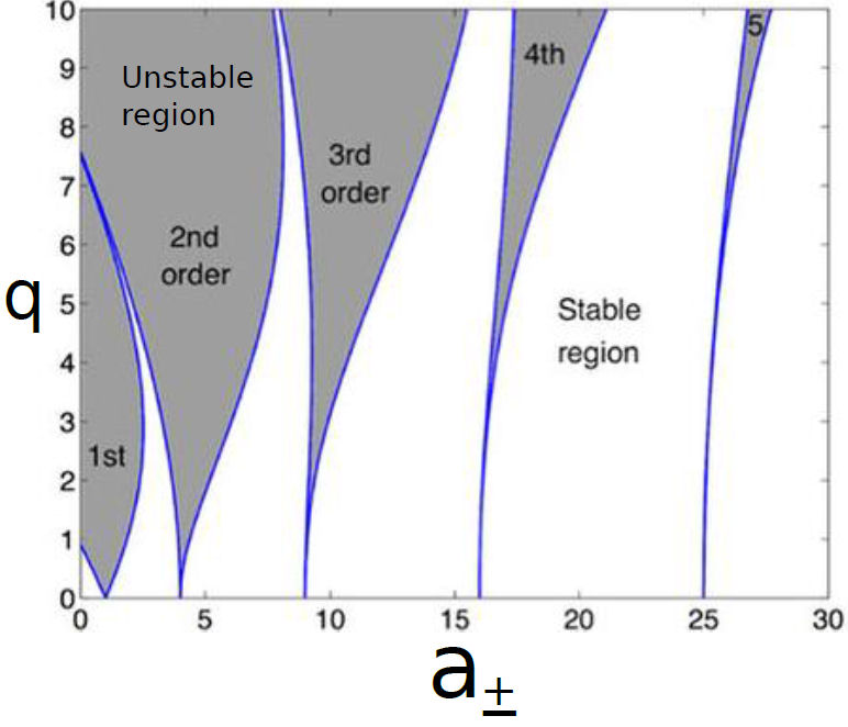
FIGURE 7 (Color online) Spectrum of the Mathieu equation showing the allowed and forbidden (shaded area) regions. The order of the gaps is indicated. This structure is known as the Arnold tongues. This diagram represents the stability of solutions for a parametric pendulum, where a ± is the ratio between the period of forcing and the natural pendulum frequency, and q is the magnitude of the external forcing.
Whenever the frequency ratio is an integer, a gap is open in the spectrum, and resonance occurs. In the present approach, the role of the natural frequency is played by the energy of an electron with a given momentum, and the forcing frequency is given by the external field. q is proportional to the field intensity; whenever q = 0, we recover the case of graphene without a field. An algebraic approach to similar problems leads to the same conclusion [81].
The important result here is that light and strain open gaps. Light induces currents and even changes the sign of the current depending on the type of polarization [73]. Moreover, we found a strong non-linear response in the sense that an ac field induces a huge content of odd harmonics allowing graphene to work as a rectifier [73]. It is important to remark that for some angles of light incidence, q can be complex, and thus the diagram looks different [74]. An interesting effect is an electron focusing by sound as gaps are open in some preferred directions [21,80,82].
3.3. Other 2D materials effective low-energy hamiltonians
Graphene paved the way to look for other effective hamiltonians. The procedure is to solve a tight-binding or perform a DFT simulation and then use an approximation around the Fermi energy. Typical examples are Silicene and Borophene. For the borophene phase with a space group 8-Pmmn, the model hamiltonian is [83]
Notice that here there are three different velocities along each coordinate axis, where by {v x ,v y ,v t } = {0.86,0.69,0.32} in units of v F = 106 m/s, and the valley index is ζ = ±1 degree of freedom, (σ x ,σ y ) and σ 0 is the identity Pauli matrix. The resulting bands are,
with eigenfunctions,
λ = ±1 denotes the valence or conduction band as in graphene and Θ = tan−1(v y k y /v x k x ) is a measure of the anisotropy. In Fig. 8, we plot Eq. (57). Two features are seen here, i) the cone is titled and ii) there is a strong anisotropy. The tilting is produced by the v t σ 0 term, while v y /v x controls the anisotropy. Both effects imply many restrictions for optical transitions, producing a very transparent material and dynamical gap opening by electromagnetic radiation [84]. To study this system under strong electromagnetic fields as well as any other periodically time-driven quantum system, we developed a very efficient and simple monodromy approach [85], which numerically is an improvement over our original analytic algebraic method [81]. The method also reproduces the results of linearly polarized light at all field intensities, for which we were able to find an exact solution [86]. Finally, this kind of hamiltonian holds in general for other anisotropic honeycomb lattices, including mechanical, acoustic, microwave, etc., analogous systems [77].
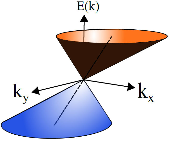
FIGURE 8 Energy dispersion in borophene resulting from the hamiltonian (55) near one of the Dirac points. The cone is tilted and anisotropic.
Interesting models are obtained by decorating graphene. An example is the α − T3 graphene, in which an additional molecule or atom enters at the center of each hexagon, coupling with just one bipartite sublattice [87-89]. Interestingly, this is the minimal model that presents flat bands coexisting with Dirac cone states. The α − T3 Hamiltonian low energy approximation is [90],
with
where
When considering the optical and electronic properties, this model behaves as a three-level Rabi problem [91].
2D Materials can also be periodically modulated when interacting with substrates. An example is the Kekule pattern seen in graphene [92]. The model can be written as [93],
or H = v 0(k·σ)⊗τ 0+v F ∆0 σ 0⊗(k·τ), where τ = (τ x ,τ y ) is a second pair of Pauli matrices, τ 0 the unitary matrix, and ∆0 is the energetic parameter that measures the strength of the bond modulation. The corresponding spectrum is
where α = ±1 labels the conduction and valence bands. β = ±1 is a label used to define two velocities, s β = (1 + β∆0).
The energy dispersion folds each graphene’s valleys into the Γ point of the Brillouin zone. This results in two cones that have the same tip, but one cone has a fast Fermi velocity v F (1 + ∆0), and the other a slow velocity v F (1 − ∆0). The eigenfunctions are [93,94],
where |Ψ α i is the graphene’s single-valley eigenvector. This model has several important features. As both valleys have the same Dirac point in momentum space, it allows to perform valleytronics by strain [18], a fact recently confirmed experimentally [95]. Also, clear signatures are seen in the optical/electronic conductivities [94,96] and plasmons due to the Moiré interference between the two-electron gases with slightly different velocities [30]. The inclusion of secondneighbor interactions modifies the picture as a gap opens in one of the cones [97].
4. Multilayered 2D materials
Multilayered materials are made by the successive stacking of 2D layers [98,99]. Figure 9 presents the results of stacking two and three graphenes. In Fig. 9b)), the B atoms of layer 2 (B2) lie on top of layer 1 A atoms of layer 1 [100,101]. Figure 9c) presents the structure of an ABA trilayer. We can identify in Fig. 9 that the electronic properties of 2D stacked materials are ruled by:
Intralayer interactions and geometry on each monolayer.
The kind of interactions between monolayers, known as interlayer interactions.
The stacking geometry, defined by a translation and rotation.
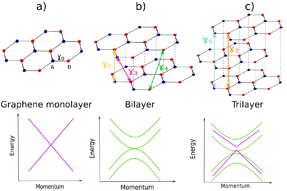
FIGURE 9 Unstrained lattice structure (upper panels) and a sketch of their corresponding energy dispersion (lower panels) for a) monolayer graphene, b) Bernal stacked bilayer graphene, and c) Bernal stacked trilayer graphene. Blue atoms belong to the A bipartite lattice, while red atoms belong to the B lattice. The arrows indicate the different kinds of interactions that appear in a TB calculation, parametrized by t 0 for intra-layer interaction, and γ i with i = 1,...,5 for inter-layer interactions. The Dirac cone seen in a) for graphene is replaced by parabolic bands in b), while trilayer graphene includes both types of bands.
In graphene over graphene, the interlayer interaction is due to Van der Waals forces, but the stacking geometry leads to complex electronic phases [11]. For graphene stacked over a metallic substrate as Au, Ag, Cu, etc., strong hybridization is seen. Even impurities can induce bond order as the Kekule patterns [102].
A typical example of a heterostructure hamiltonian is the Slonczewski-Weiss model [103]. Therein, the parameter t 0 is the usual intra-layer graphene’s interaction, as indicated in Fig. 9b). For bilayer graphene, five hoppings γ i with i = 0,...,4 account for the possible overlaps of π-orbitals.
Four on-site energies
where f(k) is given by Eq. (15). The bands resulting from diagonalization of such matrix are presented in Fig. 9b). Trilayer graphene is treated in a similar way. The energy dispersion seen in Fig. 9c) mixes the monolayer and bilayer case.
5. Superlattices: twisted and displaced graphene bilayers
Now consider the effects of the stacking geometry due to displacements or rotations. Structures known as Moiré pat- terns are produced. At certain angles, periodic superlattice are seen with a unitary cell which usually ranges from 1 to 30 nm [104,105]. Usually, the strain also appears to minimize the elastic free energy. A complete treatment of the problem requires to include not only the electronic energy but the elastic energy as well [13,14,106]. Another interesting way to build superlattices is to consider spatial variations of external electric and magnetic fields [107-110].
Needless to say, the resulting physics is rich. As examples, we have the first experimental observation of the complete Quantum Hall topological phase diagram [111], multiflavored Dirac fermions [31], and quantum phases similar to those seen in high T c superconductors [11]. This last surprising behavior is due to the appearance of flat bands at certain geometrical configurations. Both characteristic behaviors are seen in their most simple form by using a model produced by our group many years ago and that we reproduce in the following subsection [13].
5.1. Quantum Hall effect, flat bands and topology in graphene superlattices
An example of clever use of a Moiré superlattice is the experimental observation of the Hofstadter butterfly [111]. Such fractal spectrum was predicted to occur for electrons in a 2D lattice under a constant magnetic field [112]. From there, the Quantum Hall effect (QHE) was explained in terms of topological phases [113]. Recently, this phase diagram was found using higher-dimensional projections [114], or even more surprisingly, from symbolic sequences, billiards, or Sturmian codings of the magnetic flux, allowing to decode the global fractality of the spectrum and making clear the connection with quasicrystals [115]. Originally, the problem without a lattice was studied by Landau, giving levels with energy E = (n + 1/2)ℏω and n integer. In a lattice, the interatomic distance adds a new scale in the problem that competes with the magnetic length [112]. The spectrum is controlled by the ratio between the magnetic flux and elementary quantum flux. The problem translates into a one dimensional Harper equation, similar to that seen for uniaxial strained graphene [13]. For atomic systems, it was impossible to measure the Hofstadter butterfly as the ratio between fluxes is too low for any real magnetic field. The trick was to build a superlattice using a rotated substrate [111]. This allows increasing the unitary cell size and thus the flux by a dramatic amount while keeping the magnetic field accessible to available laboratory conditions [111].
Let us present a simple model able to capture such behavior. As shown in Fig. 10, suppose graphene over a substrate in which the interaction will induce deformation of graphene. We suppose that the deformation is position-dependent only in one direction, a situation known as uniaxial strain. One can take advantage of the uniaxial property by noting that graphene nanoribbons hamiltonians map into one dimensional effective chains [13] as sketched out in Fig. 10. Consider a nanoribbon in which the atoms’ positions r j are transformed by the deformation into r j +au(r j ), where u(r j ) is any general strain field. Here we demand the field to be uniaxial u(r) = (0,u y (y)). As seen in Fig. 10, the symmetry along the non-strained direction, chosen as the x direction, is not broken. The solution to the Schrödinger equation can be proposed as Ψ(r’) = exp(ik x x)ψ(y). The resulting hamiltonian thus depends upon k x and is labeled as H(k x ).
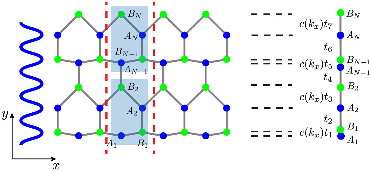
FIGURE 10 (Color online) A zig-zag nanoribbon modulated by uniaxial strain as described by Eq. (66). The wavy line to the left is the applied strain in the y-direction. The dotted line represents the period in the x direction. A vertical dotted line indicates the limits of the unitary cell in the x direction. Carbon atoms positions in the cells are labeled with A j and B j , corresponding to the bipartite lattice and j is the atom-numbering in the vertical direction. The system maps into a chain joined by effective bonds t j and c(k x )t j . At a special k x value, c(k x ) = 0 and the system decouple into dimers.
The non-strained case can be thought in terms of cells with four kind of sites (see Fig. 10] and focusing attention to the right of Fig. 10, one notes that all sites within the periodic supercell become inequivalent along the y direction when strain is applied. One labels them as A j and B j , where j is an index for the position in the path, and A or B labels the original bipartite lattice in the absence of strain.
The resulting hamiltonian is that of a one-dimensional modulated chain [13]:
where a j , a † j and b j , b † j are the annihilation and creation operators in the A and B sublattices, respectively, and N is the number of sites in the A sublattice along the periodic path. For odd j, the effective bonds are defined through:
and for even j as:
where the Grunesissen parameter is β ≈ 3. The factor c(k x ) contains the phase in the x−direction:
Figure 11 presents the resulting energy dispersion E(k x ) and the corresponding DOS for the hamiltonian (11) using a periodic substrate using a strain field u(y) = λ(0,cos(2πΛy)). Here Λ controls the spatial wavelength of the deformation and λ its amplitude. Figure 11 panels c) and d) presents the spectrum and DOS for an irrational Λ with respect to the graphene’s unitary cell distance. The spectrum presents a flat band. The model allows to track the origin of the celebrated flat-band to find that they are due to lines of quantum dots which confine states [13]. Also, the Van Hove singularities of unstrained graphene (panels a) and b)) spread along the spectrum producing peaks. For a conmmensurate Λ we can obtain the spectrum and DOS shown in Fig. 11 panels e) and f). The spectrum shows a gap, and the DOS indicates that the system decouples into linear chains, resulting in a Luttinger liquid. Figure 11 indicates the amazing possibilities as we can tune the system to be semimetallic, metallic, or insulator by using strain or a suitable substrate.
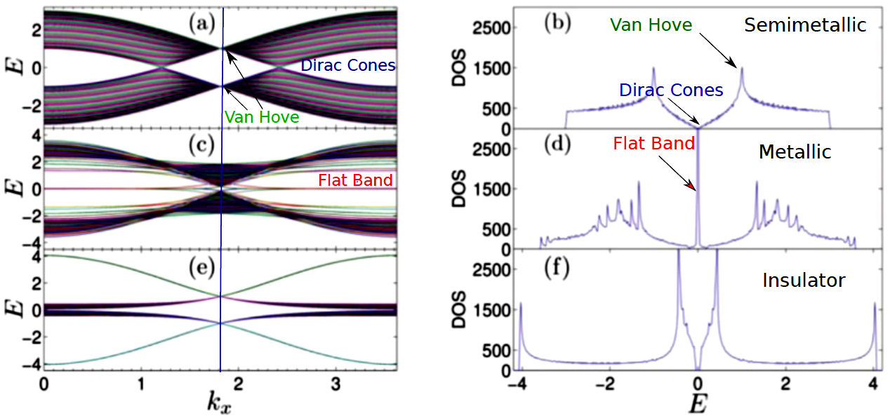
FIGURE 11 (Color online) Left columns, energy as a function of k x , and right columns, the corresponding DOS for uniaxial strain in graphene as described by the hamiltonian Eq. (66). Panels a) and b) correspond to unstrained graphene, panels c) and d) contain an incommensurate strain for the unit cell. Panels e) and f) are for conmmensurate strain. On each DOS we include labels to denote the conductivity behavior: semimetallic for graphene, metallic for incommensurate strain and insulator for commensurate strain. The Van Hove singularities and Dirac cones are indicated, as well as the flat band that appears at E = 0 for c) and d). A vertical line going through panels a),c) and d) indicate the special moment k x = 2/√ 3a where the equations are decoupled. Observe how the Van Hove singularity for graphene is a highly-degenerated dimerized system, while the effect of the strain for the incommensurate case is to spread the states forming many peaks and a flat band due to lines of quantum dots. In case f), the commensurate strain produces a gap and Van Hove singularities at band edges. This case results in two effective linear chains forming a Luttinger liquid.
An interesting situation arises for
The previous model contains interesting consequences for electronic localization [13] and non-trivial topological properties. To show the non-trivial topology, consider again a strain field u(y) = λ(0,cos(2πΛy)). For a wavelength such that Λ = 1/(2a), t j takes only two values. By performing a Fourier transform of Eq. (66) using:
and
the hamiltonian becomes:
where σ x and σ y are the x and y Pauli matrices,
and
Equation (72) is the celebrated Su-Schrieffer-Heeger model for polyethylene [117]. Therefore, non-trivial topological phases are seen for amplitudes λ > 1/2. For a gapless case (λ < 1/2), the topological modes are flat bands joining Dirac points with opposite topological charges [106,118], as happens in Weyl semimetals [119,120].
Also, this 1D model can be used to study time-dependent strain. The results lead to very complex topological phase diagrams, with new kinds of topological modes which are still in the process of being investigated [121-123].
5.2. Magic angles and superconductivity
As seen in Fig. 12, we can build a Moiré pattern by stacking graphene on top of graphene rotated by an angle θ. Let us derive the corresponding hamiltonian. For simplicity, we only consider a single valley. The hamiltonian is made from two rotated single layer Dirac hamiltonians and an interlayer coupling between them,
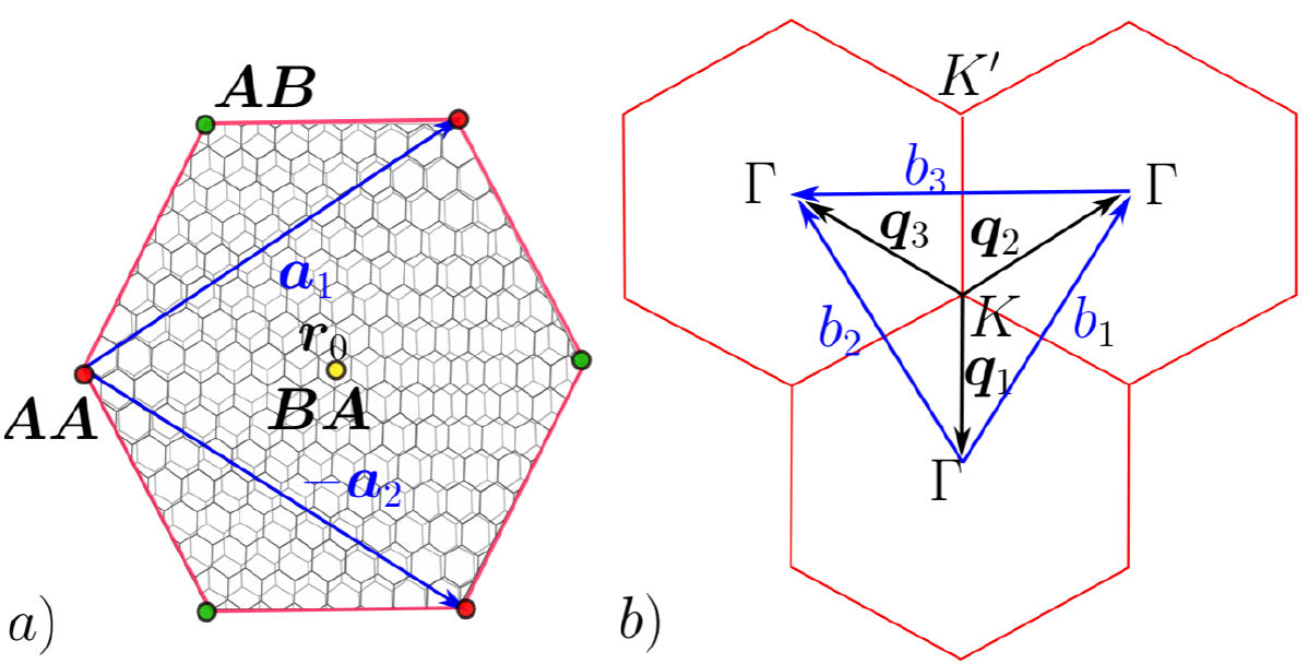
FIGURE 12 Panel a), twisted graphene over graphene geometry. The stacking points AA, AB, and BA (denoted by r0) are indicated. The Moiré vectors a 1,2 are indicated. Panel b), the Moiré Brillouin zone (usually known as a mini-Brillouin zone). The K point is at the origin. The reciprocal Moiré vectors are b 1,2 and the translation vector b 1,2,3 . The K’ point is given by K’ = K−q1.
The up (U) and down (D) labels are used to denote each layer, and
are the two rotated versions of the single-layer original Dirac hamiltonian. We have taken into account the shift of the K + Dirac point to produce the high-symmetry points K U and K D on each layer. Also, we defined two rotated versions of the Pauli matrices,
The Dirac points are now coupled together by an interlayer hopping term such that H DU = H UD † with [9],
where T 0(r),T AB (r),T AB (r) are the tunelling matrix elements. To gain a better understanding of how to build these terms, we consider first the case in which electrons tunnel only when the atoms of both layers coincide or when an atom coincides with the center of a hexagon in the other layer. As seen in Fig. 12, there are three cases: both bipartite lattices coincide, as in the stacking points AA or in an equivalent way BB, the A atoms of the upper layer align with the B atoms of the layer (AB stacking) and viceversa (BA stacking). The AA stacking points form a triangular lattice and unfavour tunneling between lattices. The AB and BA points form two sublattices of a big Moiré honeycomb. Therein, the electrons are prone to interlayer tuneling, a fact that will prove to be very relevant for the phenomenology of the system.
Now consider, for example, theP AA stacking point; the tuneling is given by
where w 1 is the energetic cost of tunneling at the AB and BA points.
In the real system, the interlayer hopping t
UD
(r) is a continuous function of the position, and thus we need to include in the sums over the Moiré reciprocal vectors a modulation factor
Defining the vector q 1 = K U −K D = k θ (0,−1) and the vectors related by ϕ = 2π/3 rotations q 2 , q 3, the interaction between layers is now written as,
with the following definitions,
where the Moiré lattice vectors a 1 ,2 and reciprocal lattice vectors b 1 ,2 are (see Fig. 12],
After all these transformations, we finally obtain the celebrated Bistritzer-Mac Donald (BM) model [9],
where,
and which has the translational symmetry,
The phase between the top and bottom layers acquired under translations can be understood as an effect of the graphene Brillouin zones twisting, as the momenta in the bottom layer are shifted by q
1 relative to the top layer. This generates the phase shift
where K’ = K − q1 is the Moiré K’ point wavevector in terms of the Moiré K point wavevector and u k(r) is a periodic function such that u k(r) = u k(r ± a 1,2 ). For zero tunneling, or large angles, the states at K and K’ correspond to the top layer and bottom graphene layer, respectively.
The spectrum of the (BM) model presents flat-bands for several θ; these are known as magical angles. As flat-bands imply localization, Bistritzer-Mac Donald suggested an enhanced electron-electron interaction at these angles and the possibility of having superconductivity [9]. Such hypothesis was experimentally confirmed in 2018, and surprisingly, the quantum phase diagram was found equivalent to those seen in high critical temperature superconductors [11]. There are many open questions in this field, and one of these is the origin of magic angles. To tackle this question, in 2019, Tarnopolsky et al. introduced a simplified version of the BM hamiltonian by making a very useful approximation [12]. They switch off the AA coupling completely by setting w 0 = 0. This results in a chiral version of the original BM hamiltonian,
where the zero-mode operator is,
and
with
The corresponding parameters are q1 = k θ (0,−1),
and
the Moiré modulation vector is k θ = 2k D sin(θ/2) with k D = (4π/3a 0) is the magnitude of the Dirac wave vector and a 0 is the lattice constant of monolayer graphene. The physics of this model depends upon the intensity of the parameter α, defined as α = (w 1 /v 0 k θ ). Here w 1 is the interlayer coupling of stacking AB and BA, and takes the value w 1 = 110 meV, while v 0 is the Fermi velocity, with value v 0 = (19.81 eV/2k D ). At magic angles α =0.586,2.221,3.751,5.276,6.795,8.313,9.829,11.345,... flat-bands appear. These magic α’s have a 3/2 cuantization rule [12] for α > 0.586 .
The chiral hamiltonian captures the “true magic” of the magic angle physics. At point AB the K point wave function has a node [12], and thus flat-bands wave functions are written using Jacobi theta functions, close to the lowest Landau state in the Quantum Hall effect [12]. Interestingly, using this model, one can predict the magic angles for any system with more than two layers [124]. Very recently, this result has been experimentally confirmed as superconductivity was found exactly at the predicted angles for trilayer graphene [125], resulting in the strongest coupled known superconductor with a large Pauli limit violation and reentrant superconductivity phases [10].
Also, recently, Naumis et al. showed that the chiral hamiltonian could be further reduced to a 2 × 2 matrix, bringing to the front the nature of frustration and the topology of the system [53]. To do this, we start with the Schrödinger equation
As before, this transformation removes the particle-hole symmetry, which is an anti-unitary anti-commuting symmetry. The resulting 2 × 2 effective hamiltonian H 2 =
D ∗(−r)D(r) is [53],
The norm of the potential is,
where b1 ,2 = q2 ,3 − q1 are the Brillouin zone Moiré vectors and b3 = q3 − q2. In Fig. 13 we present a contour plot of such effective potential, showing its trigonal symmetry and the structure of minima and maxima that produce a quantum dot effect by confining electrons. Also, notice the similarity of this function with the frustration function F(k) of graphene. The off-diagonal terms are,
and
where ∇† = −∇ with ∇ = (∂
x
,∂
y
) and µ = 1,2,3 as eigenvalues are reals (notice that −A
†(−r) = A(r)). The unitary vectors
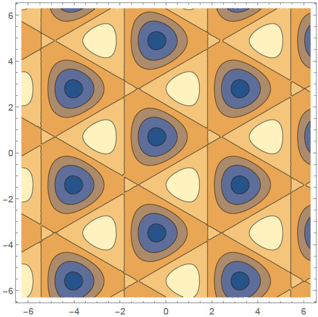
FIGURE 13 Contour plot of the effective potential Eq. (94). Observe the trigonal symmetry. For the first magic angles, the flatband states wave functions tend to confine by tracking the minima of this function, here in blue. The three-light brown maxima around each minimum act as potential barriers which confine the wave function, leading to a quantum dot effect.
6. Conclusions
A general overview of the electronic properties of 2D materials was provided making contact with the Dirac and Weyl equation approaches. We made special emphasis on the underlying frustration that produces the Dirac cone, a fact usually bypassed in the literature but that our group in Mexico pursued systematically. Moreover, this physical mechanism is in play for twisted graphene bilayers at magic angles, where superconducting phases are observed. We also reviewed a very simple mapping of graphene superlattices into a one-dimensional model that allows to recover the main features of twisted graphene over graphene, like flat-bands, topological states, fractal quantum phase diagrams, etc. Finally, we provided an overview of the physics of twisted bilayer graphene, including a recent derivation that simplifies the problem and brings the physical and topological origin of flat bands to the front [53]. In this review, we emphasized the collaborations made with other groups working in Mexico. Many of these contributions not only helped to understand 2D systems but allowed to develop new techniques to deal with periodic time-driven quantum systems, timedriven topological systems and methods to quantify frustration, build topological phase diagrams and obtain its physical properties. Among these, it is of special importance in all fields of physics the finding of an exact method to build the effective Hamiltonian of quantum time-driven systems, allowing, for example, to solve analytically the quantum harmonic oscillator with time-dependent frequency, i.e., the quantum parametric pendulum, for which solutions were not known [81].

