


 nueva página del texto (beta)
 Inglés (pdf)
 Artículo en XML
 Referencias del artículo
 Enviar artículo por email
 Citado por SciELO
  Similares en
SciELO
Similares en
SciELO 
 Permalink
1 Introduction
It is well known that cryptographic algorithms like Elliptic Curve Cryptography (ECC), and ElGamal use modular multiplication; especially the modular exponentiation uses modular multiplication. For instance, among other algorithms, RSA is the most used, since proposed by Rivest, Shamir, and Adleman in the year 1977 at the MIT [16].
RSA is based on the modular exponentiation to encrypt and decrypt critical data. Regarding this mentioned algorithm, it can be said that the main operation used is modular multiplication.
Even so, some difficulties are dealing with division and modular reduction. However, proposals like those made by Brickell [3], Barret [1], and Montgomery [11] help to solve somehow these problems and they are widely cited by many authors in the literature.
After this, it can be said that the Montgomery modular multiplication is the most efficient algorithm for modular multiplication, so the proposal made in this paper will deal with it.
The regular procedure used in this algorithm begins with a translation of the conventional representation of positive integers and brings back this translation to its original conventional integer representation at the end of the multiplication procedure.
Besides, Montgomery modular multiplication replaces the trial division with a series of additions and divisions by a power of 2, this makes it suitable to be implemented in programmable devices, like Field Programmable Gate Array (FPGA) [20, 2, 9, 19, 14]. Divisions by the power of two can be made by making only shifts to the right.
This considerably reduces the consumption of resources on the programmable device. In the search for solving issues like those mentioned above, many authors have proposed some architectures, for example, Karatsuba based Montgomery modular multiplication [4, 7], Carry Save Adders (CSA) [8, 18, 6], Compact Signed Digits (SD) [15], and Systolic Architectures [2, 9, 19, 14, 17, 21, 5], to speed up the modular multiplication.
Specifically, the proposal Karatsuba based Montgomery modular multiplication is a high speed modular multiplication, it requires a few clock cycles compared with other proposals. However, it requires a large consumption of dedicated multipliers and resources. CSA is an interesting proposal since it uses only digital logic and no dedicated multipliers.
However, it requires a large consumption of resources and clock cycles to do the modular multiplication. Among these proposals, the Systolic Architecture is particularly interesting because it has a balance between the two earlier proposals. It reduces the resources compared with CSA and reduces the dedicated multipliers compared with Karatsuba-based Montgomery modular multiplication. To do the mentioned before, Systolic Architecture uses regular blocks called Processing Elements (PEs).
For example, authors like Guilherme Perin et al. [14] , compared a high radix systolic architecture with a high radix multiplexed multiplication in an FPGA. Amine Mrabet et al. [12] proposed the implementation of the Coarsely Integrated Operand Scanning (CIOS) method of Montgomery modular multiplication using a two-dimensional array of PEs. Hence, an improvement of PEs is presented in this work, from which the associated process can be speeded up and the resources used in the FPGA are reduced as well. For this, a Montgomery modular multiplication is implemented that can deal with long integers within the finite field
This will be explained in the next section. The rest of the paper is organized as follows: Section 2 reviews the Montgomery modular multiplication algorithm and shows the improvements made. Section 3 shows the architecture proposed for implementation in an FPGA. In section 4, it is implemented the proposed architecture in modular exponentiation for use in the RSA algorithm. In section 5, it is presented the results obtained of the implementation and it is presented a comparison with other works reported. Finally, in section 6, we make the conclusions of this work.
2 Montgomery Multiplication
To perform a modular multiplication, it must have a residue of a division of the multiplication of the two positive integers. However, the arithmetic division is an operation that consumes high resources and time in hardware and software implementation, to avoid this there is a proposal called Montgomery modular multiplication algorithm [11].
The Montgomery modular multiplication is an algorithm that can be used to perform the modular multiplication
2.1 Software-base Montgomery Multiplication
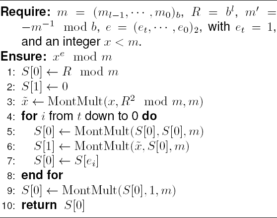
First, from the software point of view, Montgomery modular multiplication implementations use Algorithm 1, shown next, which is the original algorithm [10]. This algorithm is the basis of many RSA software and hardware implementation systems.
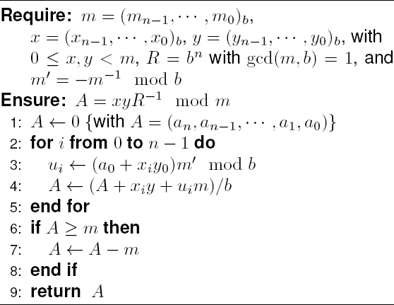
In Algorithm 1, the operands
Initially, it is required that
In modular exponentiation these added operations are inexpensive since they are done one time after the whole exponentiation. Since the mathematician Peter L. Montgomery published his algorithm in 1985, a lot of improvements were proposed by much research. The next section explains one of these approaches for hardware implementation.
2.2 Hardware-based Montgomery Modular Multiplication
On the other side, from the hardware point of view, FPGAs have been widely used to perform readily modular multiplications. It can be found proposals using several techniques that can improve Montgomery Multiplication implemented in FPGA [11, 20, 13]. One of these proposals is particularly interesting because it avoids the final subtraction used in the original algorithm [20]. To achieve this,
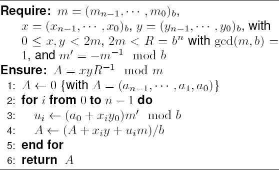
As was mentioned earlier, there is a technique that was proposed for the implementation that performs the Montgomery modular multiplication. This technique, called Systolic Architecture, uses a regular array based on a basic elemental PE. Therefore, an advantage is taken from the fact that operands are represented in a radix
Each PE internally contains multipliers and adders, which manage large operands in a multi-precisión context, based on Algorithm 2. Specifically, PEs are settled in a one dimensional array, all being identical, this was first proposed by Tenca et al. [17].
Their Montgomery multiplier has a scalable architecture, and it is based on the Multiple Word Radix-2 Multiplication Algorithm (MWR2MM). As was mentioned before, a Systolic Architecture can reduce the resources needed for the hardware implementation. Besides, it is possible to increase the number of bits of the operands adding only the required PEs for the specific dimension.
3 Systolic Architecture Proposed
Talking about the structure of the implemented system, a systolic architecture consists on a one-dimensional array of PEs [9, 20, 13], most of them are identical, the only different PEs are the first one and the last one, this will be explained Ylater.
The proposed architecture is based on Algorithm 2, where the operands are divided into
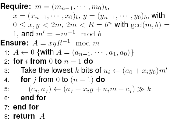
The array of PEs performs step 4 outlined in Algorithm 2, this is,
Since the systolic architecture works in a multi-precisión context, each PE is responsible to perform the arithmetic operations of each word involved in the equation, step 5 in Algorithm 3.
The value
The operation of step 3, this is,
The MMC block is designed to supply the corresponding words to the one-dimensional array of PEs and the block CU. The logic implementation of the MMC is shown in Algorithm 4 4. The MMC implemented works as follows:
– State 1: Variable
– State 2: The first PE is enabled while at the same time this PE enables the second PE, and this sequence is followed until the last PE is enabled.
– State 3: Here,
– State 4: In this state,
– State 9: This state ends the cycle and returns the result of the multiplication.
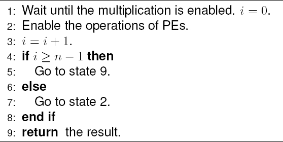
While states are performing within the MMC, Block CU is calculating at the same time the value of
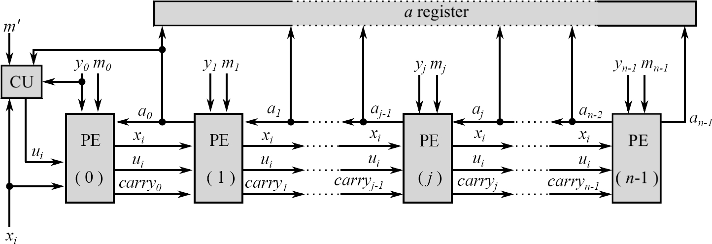
In Fig 1., the value
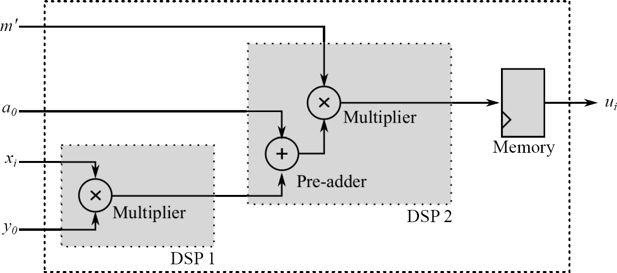
To reduce resources, and area, and speed up the implementation of the PEs, it has been used Digital Signal Processing slices (DSP) integrated into the FPGA. For our implementation in the family Artix 7 of Xilinx, it is used DPS48E1. The main features of these DSPs are that they have internally a 25 × 18 two-complement multiplier and a 48-bit accumulator.
This DSP indicates that the maximum radix that can be implemented is with 18 bits, however, in this work 16 bits were used. Description of the elements in Fig. 1 is as follows: PE(0) is an IPE, PE
3.1 Initial Processing Element
This first type of PE is called Initial Processing Element (IPE) and has direct communication with the MMC block. It receives an enabling signal, together with the value of
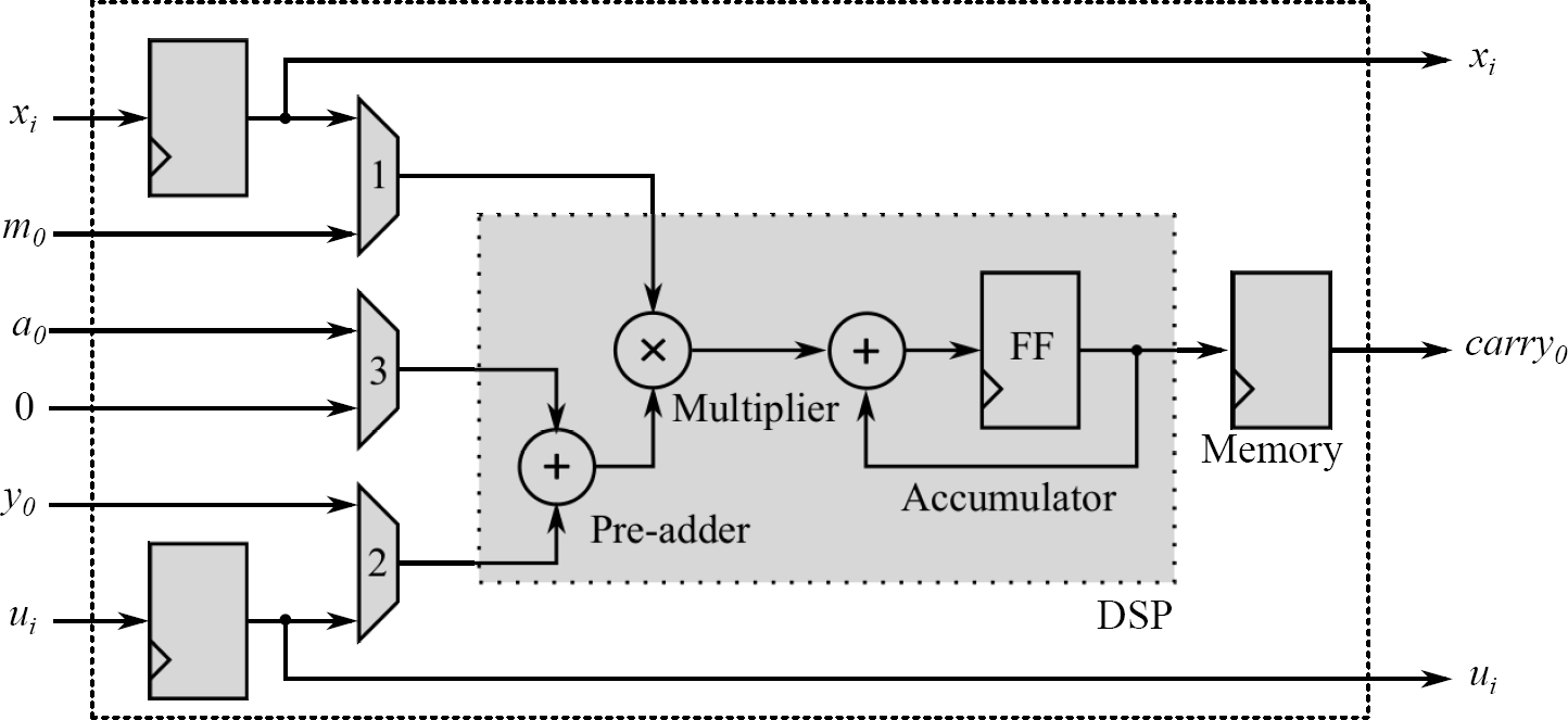
The performance of the IPE block is controlled by an FSM, which consists of three states. The performance is explained as follows: During the first state,
While yet in this first state, values of
Next, during the second state the multiplication of
However, the first
To save resources and speed up the operations, a DSP has been used as a
3.2 General Processing Element
The second type of PE is called General Processing Element (GPE). The GPE unlike the IPE receives as input a carry and gives the output
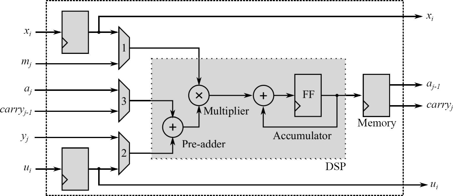
The result, the same as in an IPE, has a length of
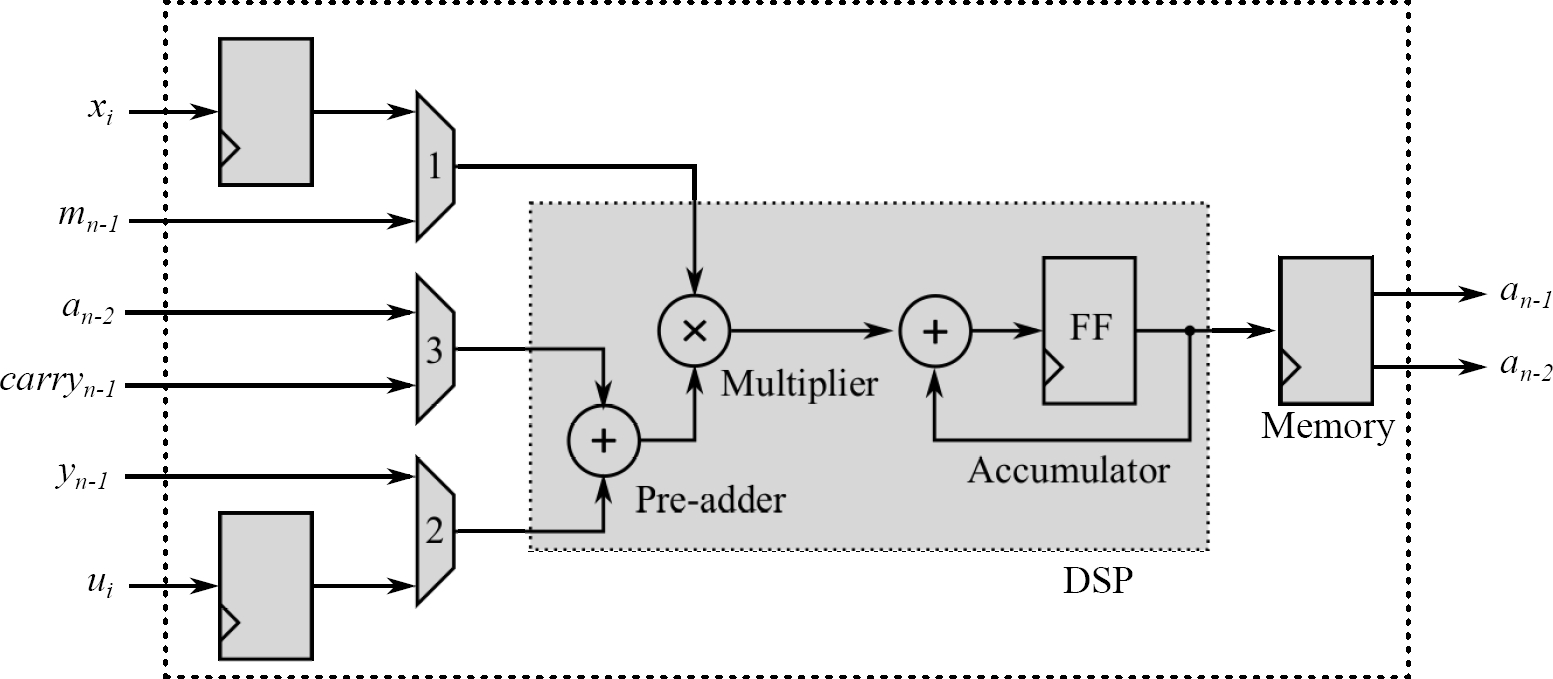
3.3 Final Processing Element
The third and last type of PE is the Final Processing Element (FPE). The performance of this type of element is like GPE, however, the output carry of this PE is avoided. The block diagram of this PE is shown in Fig. 4. As we mentioned before, the output carry is avoided, and the output of this FPE has a length of
3.4 Block CU
Finally, the block named CU calculates the value
4 Modular Exponentiation
In this section, modular exponentiation, which uses the modular multiplier proposed, is implemented into an FPGA. The modular exponentiation implemented is the Square and Multiply Always, Left to Right (SMAL2R). Algorithm 5 shows the regular modular exponentiation Square and Multiply Always algorithm and it is in a left-to-right form. This form begins the exponentiation with the most significant bit (MSB) of the exponent e and ends with the least significant bit (LSB).
From Algorithm 5, it is required that
An FSM was implemented to control the Montgomery modular exponentiation. In Fig. 6, it is shown the general block diagram which shows the implementation in FPGA. In Fig. 6 the block labeled as Control is the FSM which controls the whole modular exponentiation according to the exponent
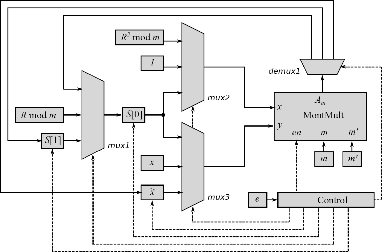
The block labeled as MontMult in Fig. 6 holds the modular multiplication proposed. The operands for this block are set by the block Control. RSA algorithm was chosen to provide both the public key and the private key. From the RSA algorithm, the value
To decrypt the data encrypted, the same modular exponentiation is used, however, the exponent is now
Since
The two extras multiplications in 3 are due to steps 3 and 9 in Algorithm 5. Once the blocks were defined and the function of each one was explained, implementation on a FPGA was made and results are presented in the following section.
5 Results
The proposed design was implemented into an FPGA Artix-7 XC7A100T-CSG324 working at 100 MHz; no area or speed optimization was set for the synthesis. The synthesis into the FPGA for the proposed design was settled to a module
First, Table 1 shows the resources used for the proposed implementation of a module of 512 bits. In this case, the implementation used 1 IPE, 1 FPE, and 30 GPE’s. Table 2 shows the resources used for the proposed implementation using a module of 1024 bits. The implementation used 1 IPE, 1 FPE, and 62 GPEs. Finally, Table 3 shows the resources used for the proposed implementation using a module of 2048 bits. The implementation used 1 PE, 1 FPE, and 126 GPEs.
Table 1 Resources used by the FPGA for the montgomery modular multiplication with a module of 512 bits
| Device Utilization | |||
| Resources | Utilization | Available | Utilization % |
| Slice LUTs | 3098 | 63400 | 4.89 % |
| Slice Registers | 2670 | 126800 | 2.11 % |
| Slice | 1471 | 15850 | 9.28 % |
| DSPs | 34 | 240 | 14.17 % |
Table 2 Resources used by the FPGA for the montgomery modular multiplication with a module of 1024 bits
| Device Utilization | |||
| Resources | Utilization | Available | Utilization % |
| Slice LUTs | 6736 | 63400 | 10.62 % |
| Slice Registers | 5337 | 126800 | 4.21 % |
| Slice | 3429 | 15850 | 21.63 % |
| DSPs | 66 | 240 | 27.50 % |
Table 3 Resources used by the FPGA for the montgomery modular multiplication with a module of 2048 bits
| Device Utilization | |||
| Resources | Utilization | Available | Utilization % |
| Slice LUTs | 12854 | 63400 | 20.27 % |
| Slice Registers | 10648 | 126800 | 8.40 % |
| Slice | 5132 | 15850 | 32.38 % |
| DSPs | 130 | 240 | 54.17 % |
Additionally, the implementation takes 98 clock cycles to perform the Montgomery modular multiplication for a module of 512 bits, 194 clock cycles for a module of 1024 bits, and 386 clock cycles for a module of 2048 bits. Table 4 shows a comparison of this work with other implementations using 1024 bits modular multiplication, and a radix of sixteen bits.
Table 4 Comparison of hardware resources and performance for the montgomery modular multiplication
| Work | Device |
Module |
Radix |
Freq. (MHz) | Clock Cycles | Slice LUTs | Slice Registers | Slices | DSPs |
| Perin | Virtex-4 | 1024 | 16 | 110 | 384 | - | - | 7012 | 130 |
| Perin | Virtex-5 | 1024 | 16 | 130 | 384 | - | - | 6642 | 130 |
| Wang | Virtex-5 | 1024 | 16 | 120 | 199 | 14440 | 7826 | - | 66 |
| C.McIvor | Virtex-2 | 1024 | 16 | 104 | 199 | - | - | 5709 | 131 |
| Mrabet | Artix-7 | 1024 | 16 | 65 | 66 | 5242 | 4208 | 2072 | 161 |
| Mrabet | Virtex-5 | 1024 | 16 | 65 | 66 | 5824 | 6072 | - | - |
| Proposed architecture | Artix-7 | 1024 | 16 | 100 | 194 | 6736 | 5337 | 3429 | 66 |
From the above, it can be seen that the proposal allows a reduction of resources consumption within the programmable device, compared with other developments. On the other side, the implementation of the Montgomery modular exponentiation uses a module
The resources used by the implementation into the FPGA for the modular exponentiation are shown in Table 5. As it was already said, in this proposal, the implementation of the Montgomery modular exponentiation was used to encrypt and to decrypt data.
Table 5 Resources used by the FPGA for the montgomery exponentiation with a module of 1024 bits
| Device Utilization | |||
| Resources | Utilization | Available | Utilization % |
| Slice LUTs | 7587 | 63400 | 11.97 % |
| Slice Registers | 9499 | 126800 | 7.49 % |
| Slice | 4253 | 15850 | 26.83 % |
| DSPs | 66 | 240 | 27.50 % |
The public-key and the private-key were generated with the RSA algorithm. According to Table 4, the proposed architecture reduces 5 clock cycles compared with the performance reported in[9] and [21]. With these 5 clocks cycles, the time consumption in the Modular Exponentiation of Algorithm 5 is reduced.
For example, with
6 Conclusions
As can be seen in the tables reported, the most resources in the modular exponentiation are due to the modular multiplication, so it is important to reduce them. As we can see from the results of this work, the proposed architecture, compared with the other works that use a high-radix modular multiplication reduces the time consumption and the resources used for the FPGA, as well.
Due to this low use of resources into the FPGA, the implementation of the Modular Exponentiation and Multiplication using the proposed Algorithm can allow its use in programmable devices that have limited available resources. Therefore, the programmable device to be used will be cheaper than a high-end programmable device.
This work implements modular exponentiation for RSA cryptographic algorithms; however, it is possible to use in other cryptographic algorithms like ECC, ElGamal, DH. Even more it is possible to implement this proposal to different modular exponentiation algorithms. Besides, it is important to say also that the proposed architecture is scalable to another module. For example, making, this same procedure with a device that has more DSPs, it will be possible to increase the module to a value up-to 4,096 bits with the use of 258 DSPs.

