


 nueva página del texto (beta)
 Inglés (pdf)
 Artículo en XML
 Referencias del artículo
 Enviar artículo por email
 Citado por SciELO
  Similares en
SciELO
Similares en
SciELO 
 Permalink
1. Introduction
In the last decades, with the development of electronic devices, a technological revolution took place, leading society into a new digital era, with silicon playing the central role as the constituent element of such devices due to its properties. Essentially, silicon is a semiconductor material and the second most abundant element on earth (representing more than 25% of the Earth’s crust), characteristics that make it ideal for applications in embedded systems due to its low procurement costs [1].
There have being two main driving forces behind the development of semiconductor devices: the ever increasing need for computing power and the advancement of nanotechnology, with the former leading to progressive shrink-age of transistors and the latter allowing for the creation of the so-called nanostructures. Depending on their dimensionality, nanostructures can be organized in 0D (fullerenes, nanoparticles), 1D (nanowires, nanotubes) and 2D (germanene, graphene), presenting all of them an effect called quantum confinement, that occurs because the propagation of waves is restricted [2].
Henceforth, the necessity to reduce the size of transistors (to fabricate silicon chips) in combination with the advances made in nanotechnology led to the first successful synthesis of silicon nanowires in 1998 by Morales et al, using a combination of laser ablation cluster formation and vapor-liquid-solid (VLS) methods [3]. The necessity of minimizing transistors (to fabricate silicon chips) in combination with the advances made in nanotechnology led to the first successful synthesis of silicon nanowires (SiNWs) in 1998 by Morales et al [3], using a combination of laser ablation cluster formation and vapor-liquid-solid (VLS) methods. Subsequent studies by Holmes et al [4] and Cui et al [5] yielded SiNWs ranging from 3nm to 31nm of diameter growth in different crystallographic planes, proving that tunning the morphology of nanowires was possible. Since the first successful synthesis of SiNWs, several experimental studies have been made to survey their potential applications in solar cells [6], Li-ion batteries [7], biosensing [8], thermoelectrics [9] and optics [10]. In this regard, theoretical studies have been made mainly to explain the electronic properties of SiNWs, such as their bandgap dependence on size and orientation [11-15]. Since the synthesis of SiNWs with diameters of around 1 nm is still very challenging, most of the available experimental and theoretical studies on the electronic properties of silicon nanowires are focused on systems with large diameters, which makes it necessary to increase the efforts to study SiNWs oriented in different directions in the nanometric regime.
Regarding the optical properties of SiNWs, they are scarcely documented and the available works focused mainly on the description of the optical absorption polarizing the nanowires in different directions [16-20]. Particularly for 1D structures, it is possible to relate the absorption curves with the density of states through the Van Hove singularities [21,22], but there are no studies in which the Van Hove singularities had been used to establish a relationship between the optical and electronic properties of silicon nanowires. One of the most promising methods available to study SiNWs is the density functional theory (DFT), which is extremely useful for the theoretical calculation of the structural, electronic and optical properties of nanostructures, thanks to its relatively low computational cost (in comparison with methods that use exact N-body wave functions) and its good agreement with experiments.
In this work we performed an investigation of the structural, electronic and optical properties of a set of silicon nanowires with different diameters, oriented in the directions [001], [110] and [111]. The calculations were done using the density functional theory as implemented in the Spanish Initiative for Electronic Simulations with Thousands of Atoms (SIESTA) code [23], with a local density potential to approximate the exchange and correlation energy [24]. We polarized the system along the radial direction (Z) and along the plane XY , obtaining in each case the electronic band structure, the electronic density of states and the absorption spectrum. Finally, we analyzed the relationship between the transitions in the density of states and the peaks in the absorption spectra.
2. Methodology
This study is comprised by four stages, in the first one the nanowires were modeled: some parameters like the kinetic energy of the wave functions were adjusted using a self-consistent field calculation, after which the structures were optimized and finally, the electronic and optical properties were obtained through posprocessing. The studied structures were constructed as follows: first we cleaved a surface in a specific plane direction from the bulk structure of silicon (i.e. face-centered-lattice with a two-atom basis), then we built a crystal slab (assuring periodicity) to construct a supercell and, finally, we cut a wire with a specific diameter in which the dangling bonds on the surface with hydrogen were passivated. In addition to using different diameters for the silicon nanowires, we orientated them in the directions [001], [110] and [111]. These systems are shown in Fig. 1 and described in Table I.
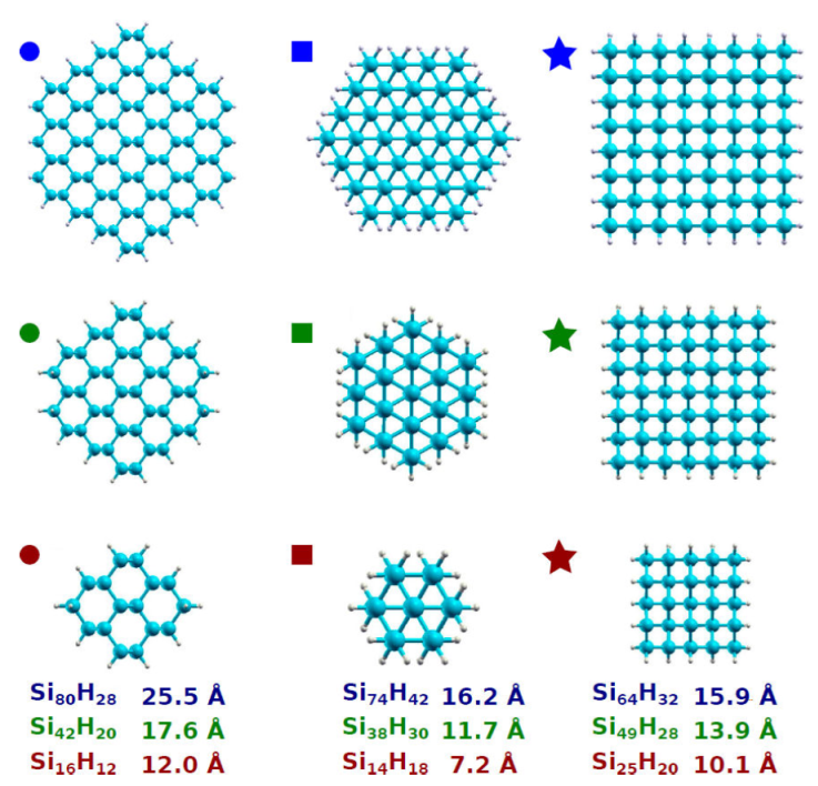
Table I Main structural and electronic properties of the nanowires shown in Fig. 1, the C parameter at the beginning (Ci) and at the end (Cf) of the relaxation process [Å], the magnitude of the bandgap (Egap ) [eV], the transition between the point of maximum energy in the valence bands (PMV ) and the point of minimum energy in the conduction bands (PMC ) [eV/atom], and the cohesion energy (Ecohesion ) [eV/atom].
| Nanowires |
|
|
|
PV-PC |
|
|---|---|---|---|---|---|
| Si16H12 | 3.825 | 3.836 | 1.814 | Γ-Γ | 8.11 |
| Si42H20 | 3.825 | 3.873 | 1.177 | Γ-Γ | 9.95 |
| Si80H28 | 3.825 | 3.866 | 0.827 | Γ-Γ | 11.12 |
| Si25H20 | 5.410 | 5.240 | 2.496 | α-Γ | 7.82 |
| Si49H28 | 5.410 | 5.306 | 1.798 | β-Γ | 9.23 |
| Si64H32 | 5.410 | 5.321 | 1.60 | μ-Γ | 9.81 |
| Si14 H18 | 9.370 | 9.069 | 3.561 | Γ-γ | 5.78 |
| Si38 H30 | 9.370 | 9.241 | 2.181 | Γ-Γ | 7.88 |
| Si74 H42 | 9.370 | 9.290 | 1.576 | Γ-δ | 9.31 |
In the second stage we adjusted the kinetic energy of the wave functions and the number of k points in the reciprocal space, for which we used a self-consistent field calculation with a Troullier-Martins local density approximation potential [25], with the core electrons represented by norm-conserving pseudopotentials in their entirely separable form, and the valence electrons represented by a double-zeta singly polarized basis set [26].
In the third stage we performed the optimization of the nanowires: the SiNWs were modeled using a tetragonal unit cell, in which the wire’s axial axis was aligned with the C parameter in the Z direction, while the A and B parameters were aligned with the X and Y axes, respectively. We set the A and B parameters to produce an empty space of 10 Å between neighboring nanowires in order to avoid interactions. The C parameter and the atomic coordinates were optimized until the forces between the atoms inside the structures were lower than 0.0001 eV/Å.
In the last stage we calculated the electronic and optical properties of the SiNWs optimized structures: the electronic band structure and the density of states were computed using the standard diagonalization method. Also, we obtained the optical absorption spectra δ ‖ in the axial Z direction and δ ⊥ along the XY plane. Finally, using the Van Hove singularities we related the peaks in the absorption spectra with the transitions in the density of states.
3. Results and discussion
3.1. Structural properties
We analyzed the structural properties of the SiNWs shown in Fig. 1, before and after the optimization processes, in order to identify deformations. Initially we modeled the silicon nanowires with a tetragonal unit cell, where the A and B parameters were adjusted to get a suitable empty space between adjacent wires along the X and Y directions. On the other hand, the C parameter was initially set identical for all the nanowires in the directions reported in Table I and presented changes after the optimization processes depending on the nanowire’s orientation and diameter. We found that the nanowires oriented in the directions [001] and [111] are compressed by the optimization process, as suggested by the reduction of their C parameters upon optimization. On the other hand, the nanowires oriented in the direction [110] were found to expand, as suggested by the expansion of their cells due to the increase in their C parameters.
The cohesion energy plays a very important role in the growth process of silicon nanowires because it influences the transport properties of the silicon atoms during that process, which means it can prevent them from diffusing properly or inhibit their transport altogether. The growth process of a silicon nanowire is a delicate process within the bottom-up approach, in which the cohesion energy of the silicon atoms plays a very important role. One of the methods for growing silicon nanowires is the VLS (vapor-liquid-solid), in which the silicon atoms present in the vapor are absorbed by a liquid catalyst. The atoms then get diffused through the liquid catalyst until they reach the liquid-solid interface, thus “exiting” the liquid catalyst and “organizing” into a new structure: the silicon nanowire, which grows upon repeating the previously described process. The strength of the cohesion energy is very important in the diffusion process of the silicon nanowires within the liquid catalyst, as can be seen in the following extreme scenarios: a very weak cohesion energy leads to a less efficient diffusion through the catalyst and a limited growth potential for the resulting nanowire, on the other hand a very strong cohesion energy might prevent the atoms from exiting the liquid catalyst altogether, thus preventing the creation of the nanowire. In order to control the cohesion energy, in this case for the creation of silicon nanowires, the following conditions can be modified: temperature (which is inversely proportional to cohesion), pressure (which is directly proportional to cohesion), the introduction of impurities or the application of external fields. To analyze the stability of the nanowires, we calculated the cohesion energy using the following equation:
where ENW , ESi and EH are the energies of the silicon nanowires, a single atom of silicon and a single atom of hydrogen, respectively. NSi and NH are the number of atoms of silicon and hydrogen in the nanowire, respectively, and NNW are the total number of atoms in the nanowire.
We analyzed the nanowires according to their orientation, and the results showed a relationship between the diameter of the nanowire and the cohesion energy. In particular, if the diameter is augmented, the cohesion energy rises as well, as seen in Fig. 2. Furthermore, the nanowires oriented in the direction [111] seem to be the less stable ones, whereas those oriented in the [110] direction seem to be the most stable.
Figure 2 Cohesion energy for the nanowires oriented in the direction [110] (blue circles), [001] [red squares] and [111] (black rumbles).
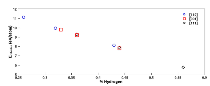
To explain the behavior of the stability in the silicon nanowires oriented in different directions, we analyzed their structure and morphology. We identified an increment of the stability in the nanowires as their size increases with the diameter. In addition, as the size of the nanowire increases, the dangling bonds on the surface decrease, which causes a reduction in the number of hydrogen atoms used to passivate the nanowire. Starting from the above information, we computed the percentage of hydrogen in the nanowires and graphed this data versus the cohesion energy, as seen in Fig. 3. Regardless of the orientation, the results show an increase in the stability of the nanowire as the percentage of hydrogen diminishes.
3.2. Band structure and DOS
The electronic band structure revealed the type of bandgap transition between the points of maximum (PMVB) and minimum (PMCB) energy in the valence and the conduction bands, respectively, for the nanowires studied in this work, as seen in Fig. 4. We divided our analysis in three parts, depending on the orientation of the nanowires. For the nanowires oriented in the direction [110], the transition between PMVB and PMCB in the three wires occurred at the Γ point, in agreement with the band folding found by Zhao and coworkers [11]. In the case of the SiNWs oriented in the direction [111], we have two different behaviors. The transition in the wire Si38H30 is direct and occurs at the Γ point. However, the transition for the wires Si14H18 and Si74H42 is indirect and happens from Γ (PMVB) to γ (PMCB) and from Γ (PMVB) to δ (PMCB), respectively. According to Rurali and coworkers, the SiNWs (oriented in the direction [111]) are semiconductors, and their transition is direct when the diameter exceeds 1.5 nm and indirect when the diameter is lower than 1.5 nm [13]; we found, however, that the transition becomes indirect again when the diameter is lower than 1 nm. This is attributed to the change in the orbitals that contributed to the total density of states. In the two bigger wires Si38H30 and Si74H42 the contribution of the orbital s is greater than the contribution of the orbital p in the direction x. However, in the smallest wire Si14H18 the contribution of the orbital p in the direction x is greater than that of the orbital s. For the nanowires oriented in the direction [001], the SiNWs presented an indirect transition.
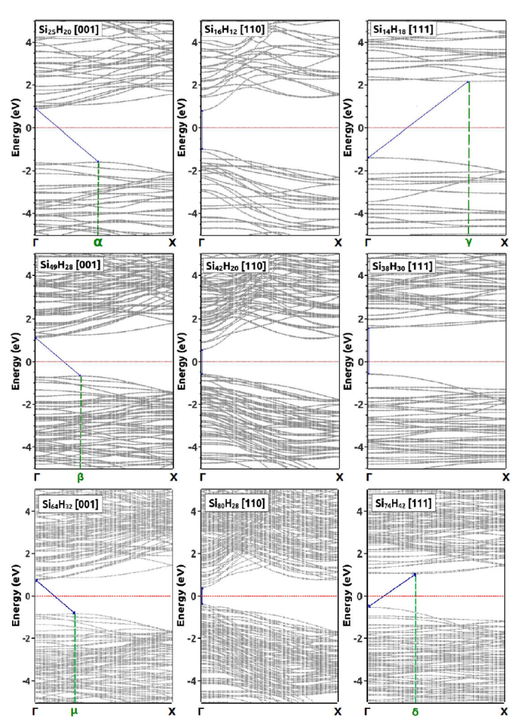
Figure 4 Electronic band structure of the silicon nanowires. The silicon nanowires oriented in the directions [001], [110] and [111] are represented in the first, second and third columns, respectively.
Finally, the magnitude of the bandgap increases when the diameter of the silicon nanowires decreases, as seen in Fig. 6, a behavior consistent with the effect of quantum confinement, in agreement with Man-Fai and co-workers [15].
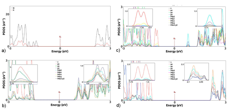
Figure 5 In this figure we show the projected density of states (PDOS) of a) silicon and hydrogen for Si 25 H20, the PDOS for orbital of silicon of the nanowires b) Si25 H20, c) Si16 H12 and d) Si14 H18. The rest of nanowires of the same orientation show a similar behavior.
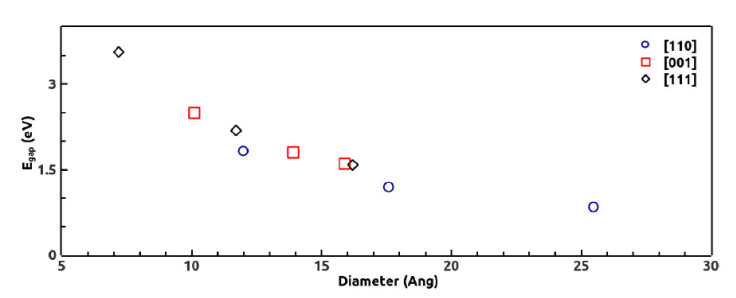
Figure 6 Magnitude of the band gap of the silicon nanowires. The silicon nanowires oriented in the directions [111], [001] and [110] are represented with blue rumbles, black circles and red squares, respectively.
In the present study, we modeled nanowires so that they are concentric in each orientation, so the morphology of nanowires oriented in the same directions is similar. On the other hand, the morphology of nanowires oriented in different directions changes. The first Brillouin zone of nanowires depends on their morphology, so nanowires oriented in different directions present different first Brillouin zone. Due to the above the electronic properties of nanowires, such as the transition between valence and conduction bands, depend on their orientation. In order to analyze how the orientation of the nanowires influences their electronic properties, we calculated the projected density of states for each nanostructure in the study. The results show that the orbitals contributing to the DOS near the Fermi level are the same in nanowires oriented in the same direction, while these orbitals are different when the orientation of the nanowires is different as we can see in Fig. 5.
In the following sentences, we will show the results of the projected density of states (PDOS). Particularly, we analyzed two zones; the first is in the valence bands region, specifically the subregion that lies near the bandgap. The second zone is in the conduction bands region, specifically the subregion that lies near the bandgap. In the successive, we refer to the valence region when we talk about Subregion 1 and the conduction region when we talk about Subregion 2. The main contribution to the total density of states (DOS) in silicon nanowires is because of silicon atoms. On the other hand, the function of hydrogen atoms is the passivation of dangling bonds at the surface of nanowires. Considering the above, we will analyze the PDOS of silicon atoms in nanowires oriented in different directions to explain their electronic behavior.
In SiNWs oriented in the direction [001] the available states in the valence region are given mainly by the orbital p in directions x, y, and z. Besides, the PDOS of orbital p in the directions x and y are equal. This last part is due to the symmetry of the nanowire itself. On the other hand, in the conduction region, the main contribution to the available states is due to the orbital d in the directions xz, yz, and xy. Moreover, the PDOS of orbital d in the directions xz and yz are equal because of the symmetry of the nanowire. In the nanowires oriented in the direction [110], the main contributions to the DOS in the valence region are done by the orbital p in direction z and orbital d in direction xz. In the conduction region near the bandgap, the available states are produced by the contribution of the orbitals d in direction z, orbital p in direction x, and orbital s. In the nanowires oriented in the direction [111] the available states in the valence bands region are due to the orbital p and d in the direction z. In the conduction region, the main contribution to the DOS is due to the orbital d in the directions xz, yz, and z, orbital p in the direction x, and orbital s. Moreover, the PDOS of orbital d in the directions xz and yz are equal due to the symmetry of the nanowire. Finally, it is important to mention that the contribution of the orbital s is greater than the contribution of orbital p in nanowires Si74H42 and Si38H30, however in nanowire Si14H18 the contribution of orbital p is greater than the contribution of orbital s to the DOS. This is cause the quantum confinement effect is stronger in orientation [111].
3.3. Optical properties
The imaginary part of the dielectric function was calculated using an approach on the dipolar transition matrix elements between the different eigenfunctions of the self-consistent Hamiltonian. We also obtained the optical absorption spectrum, particularly, we polarized the nanowires parallel to their axial Z axis and perpendicular to their axial Z axis (XY plane), and got δ ‖ and δ ⊥, respectively. The optical spectra for the nanowires are shown in Fig. 7, in which both δ ‖ and δ ⊥ are seen to shift to lower energies as the diameter of the nanowire increases, regardless of the orientation. Furthermore, δ ‖ and δ ⊥ become more different and show more anisotropy with increasing diameter.
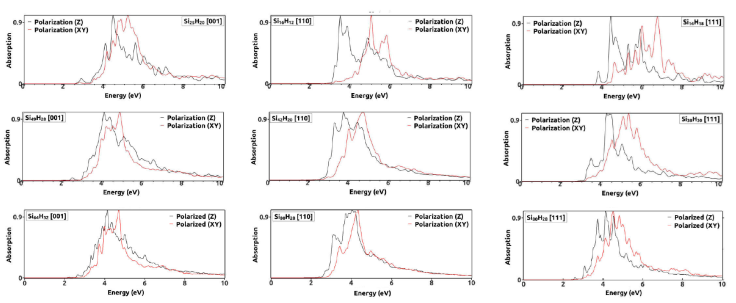
Figure 7 Optical absorption spectra for the silicon nanowires. The red curve represents the absorption spectrum when the nanowire was polarized in the direction of the XY plane. The black curve represents the absorption spectrum when the nanowire was polarized in the direction of the Z axis.
The density of states and the optical absorption spectrum are directly related, in fact for a semiconductor material (such as the nanowires in this work), the magnitude of the band gap is related to the energy in which the optical spectrum starts to show a non-zero absorption. In the case of the nanowires, the the increase in diameter makes the bandgap decrease, which in turn provokes a shift of the absorption spectrum to lower energies.
Since nanomaterials are confined, their properties differ significantly from those of the bulk, something that is especially true for nanowires with decreasing diameters. In fact, as we decrease the diameter of SiNWs, δ ‖, and δ ⊥ become more different, while an increase in diameter makes δ ‖ and δ ⊥ more similar; in bulk silicon, δ ‖ and δ ⊥ are identical because of the symmetry.
Using the theory of Van Hove singularities we found a relationship between the transitions in the density of states and the absorption peaks in δ
‖ and δ
⊥. The transitions in the density of states were analyzed for the nanowires reported in Table I and two types of transitions were identified: direct transitions and indirect transitions. The direct transitions are those that satisfy the equation 𝜖n =
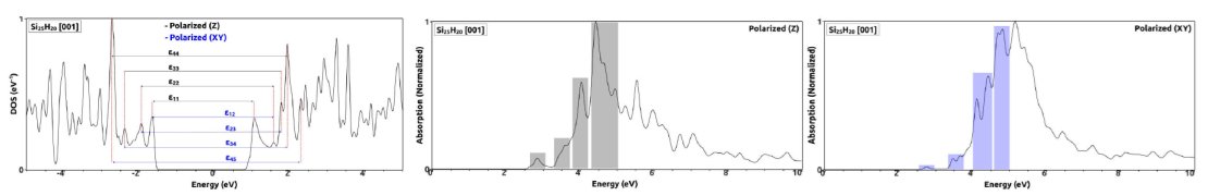
Figure 8 Transitions between the Van Hove singularities in the density of states and how they are related to the absorption spectra. The transitions that satisfy the equation a+a (black) are related to the spectrum with Z polarization and the transitions that satisfy the equation a+b (blue) are related to the spectrum with XY polarization.
Table II Direct transitions (𝜖n,n) between the Van Hove singularities in the density of states and the peaks (Rn) in the optical absorption spectrum, when the nanowire is polarized in the direction of the Z axis.
| Nanowires | Transitions in DOS (eV) | Peaks in δ ‖ (eV) | ||||||
|---|---|---|---|---|---|---|---|---|
| 𝜖11 | 𝜖22 | 𝜖33 | 𝜖44 | R 1 | R 2 | R 3 | R 4 | |
| Si25 H20 | 2.64 | 3.52 | 4.17 | 4.63 | 2.83 | 3.58 | 4.024 | 4.63 |
| Si49 H28 | 1.98 | 2.71 | 3.68 | 4.19 | 2.07 | 2.52 | 3.62 | 4.06 |
| Si64 H32 | 1.91 | 2.71 | 3.52 | 4.22 | 2.0 | 2.66 | 3.53 | 4.13 |
| Si16 H12 | 1.81 | 2.93 | 3.66 | 4.40 | 1.86 | 2.96 | 3.65 | 4.37 |
| Si42 H20 | 1.25 | 1.94 | 2.89 | 3.89 | 1.19 | 1.89 | 2.95 | 3.86 |
| Si80 H28 | 1.47 | 2.30 | 2.78 | 3.48 | 1.54 | 2.40 | 2.80 | 3.33 |
| Si14 H18 | 3.66 | 4.85 | 5.40 | 5.84 | 3.73 | 4.61 | 5.41 | 5.83 |
| Si38 H30 | 2.30 | 3.25 | 4.04 | 4.50 | 2.48 | 3.26 | 4.03 | 4.47 |
| Si74 H42 | 2.13 | 3.04 | 3.71 | 4.2 | 2.0 | 3.07 | 3.72 | 4.13 |
Table III Direct transitions (𝜖n,n+1) between the Van Hove singularities in the density of states and the peaks (Rn) in the optical absorption spectrum, when the nanowire is polarized in the direction of the XY plane.
| Nanowires | Transitions in DOS (eV) | Peaks in δ ⊥ (eV) | ||||||
|---|---|---|---|---|---|---|---|---|
| 𝜖12 | 𝜖23 | 𝜖34 | 𝜖45 | R 1 | R 2 | R 3 | R 4 | |
| Si25 H20 | 3.20 | 3.69 | 4.33 | 4.96 | 2.93 | 3.64 | 4.42 | 4.8 |
| Si49 H28 | 2.68 | 3.20 | 4.01 | 4.66 | 2.49 | 3.3 | 3.93 | 4.5 |
| Si64 H32 | 2.39 | 3.26 | 3.80 | 4.72 | 2.48 | 3.34 | 3.72 | 4.69 |
| Si16 H12 | 2.45 | 3.29 | 4.06 | 4.55 | 2.44 | 3.25 | 4.2 | 4.54 |
| Si42 H20 | 1.79 | 2.52 | 3.41 | 4.30 | 1.77 | 2.56 | 3.44 | 4.12 |
| Si80 H20 | 1.80 | 2.48 | 3.37 | 4.11 | 1.77 | 2.5 | 3.42 | 4.24 |
| Si14 H18 | 4.20 | 5.10 | 5.72 | 6.16 | 4.23 | 4.97 | 5.61 | 6.25 |
| Si38 H30 | 2.62 | 3.54 | 4.34 | 5.06 | 2.69 | 3.55 | 4.4 | 5.07 |
| Si74 H42 | 2.69 | 3.28 | 4.06 | 4.51 | 2.60 | 3.24 | 4.11 | 4.52 |
4. Conclusions
In this work, we have studied the stability as well as the electronic and optical properties of a set of silicon nanowires, oriented in the directions [110], [001] and [111]. The obtained results allow us to conclude that the stability of silicon nanowires depends on their diameter and orientation. In particular, the stability of a silicon nanowire is proportional to its diameter and, according to our results within the studied structures, the wires oriented in the direction [110] are the most stable, while the ones oriented in the direction [111] are the less stable. The calculated densities of states and band structures show that silicon nanowires are semi-conductor materials in which the bandgap depends on both their diameter and orientation: the bandgap’s magnitude is inversely proportional to the diameter of the nanowires. The type of transition in the bandgap depends on the orientation of the nanowires: the silicon nanowires oriented in the direction [001] presented an indirect bandgap, while those oriented in the direction [110] presented a direct bandgap. In some cases the diameter of the wire influences the type of bandgap due to the quantum confinement effects as we showed by calculation the PDOS, for instance, SiNWs oriented in the direction [111] have a direct bandgap for a diameter of 11.7Å and an indirect bandgap for a diameter of 7.2Å and 16.2Å. The diameter of the wires also influences the optical properties, shifting the optical absorption spectra to lower energies when it increases, as can be seen for the computed spectra δ ‖ and δ ⊥, corresponding to nanowires polarized in the direction of the Z axis and the direction of the XY plane, respectively; an increased diameter also makes δ ‖ and δ ⊥ more similar.
Finally, by relating the transitions between the Van Hove singularities in the density of states to the spectra δ
‖ and δ
⊥, we found that the transitions that satisfy the equations 𝜖n =

