


 nueva página del texto (beta)
 Inglés (pdf)
 Artículo en XML
 Referencias del artículo
 Enviar artículo por email
 Citado por SciELO
  Similares en
SciELO
Similares en
SciELO 
 Permalink
1. Introduction
The hybrid compounds type perovskite ABX3 are composed by an organic cation (A), an inorganic cation (B), and a halide (X). The most common ions used are: methylammonium (MA) as the organic cation, Pb as the inorganic cation and I as the halide. The crystalline structure of MAPbI3 is based on an octahedral PbI6 configuration, where the Pb atoms stay at the central position and I atoms occupy the vertices of the octahedron, while the methylammonium ions stand at the free spaces between successive octahedra [1]. The polarity of methylammonium and its interaction with inorganic network give to MAPbI3 unique electronic and optical properties, being widely studied because of its high potential as a semiconductor. The properties like high optical absorption over a broad solar spectrum, high carrier mobility and long carrier lifetime [2-5] make this material highly attractive. These properties, together with low-cost and low temperature production methods have promoted the development and improvement of solar cells based on this material.
Indeed, since 2009, experimental solar cells based on hybrid organic-inorganic-perovskites were fabricated, achieving efficiencies from 3.8% [1] to above of 25% [6]. Nevertheless, the hybrid perovskites degradation has been reported within a few days or hours in operation under standard conditions [7, 8], which is immediately detected by X-ray diffraction (XRD) through a drop in the (100) reflection, in case of MAPbI3 [9]. The main causes of degradation are photoreduction due to UV light (from the Sun), plus the high reactivity with environmental humidity [10, 11]. The perovskite degradation is due to the hydrophilicity and volatility of the organic cation. Additionally, UV radiation and oxygen can deteriorate the device performance [12]. To reduce the instability in MAPbI3, the iodine as well as lead can be partially replaced by chlorine and tin, respectively [12-15]. Indeed, depending on the halide used, the bandgap can be continuously tuned from 1.6 eV (pure I) to 3.2 eV (pure Cl). The chlorine drives the crystallization dynamics, with a preferential order induced during the crystallization process [16] and more uniform and dense thin films are obtained, giving more chemical stability. Additionally, Cl improves morphology increasing the charge transport [13] due to higher electronegativity [17]. To balance the increased bandgap value caused by chlorine, lead can be partially replaced with tin which reduces the bandgap (until 1.3 eV). It has been reported that the smaller bandgap materials provide the better solar cell efficiencies [11,16,18,19], being 1.75 eV considered ideal [20, 21].
The preparation method is fundamental to achieve the ideal thickness of the perovskite film (about 500 nm), and the crystalline structure. Reported methods start from the same precursors: methylammonium Iodide (MAI) and lead iodide (PbI6). Most of the bibliography reports the obtention method in two steps: first a layer of PbI6 is deposited on the substrate and then the MAI is deposited on the PbI6 by evaporation [22]. Nevertheless, the CH3NH3PbI3 perovskite formed by vapor deposition can involve unexpected chemical reactions and competing processes [15]. In a previous work, we obtained thin films of MAPbI3 by deposition, in one step, of a 1 molar solution containing both precursors, MAI and PbI6 in N-N-dimethylformamide [23].
In this work, we reported the synthesis and characterization of the doped hybrid perovskites, CH3NH3Pb0.9 Sn0.1I2.8Cl0.2 and CH3NH3Pb0.75Sn0.25I2.5Cl0.5. Stands out the improvement of stability under environmental conditions.
2. Methodology
The hybrid perovskites CH3NH3Pb0.9Sn0.1I2.8Cl0.2 and CH3NH3Pb0.75Sn0.25I2.5Cl0.5, were synthesized at environmental conditions, 25
The chemical attack involves three mains steps, first the substrates are cleaning with soap phosphates free and water. They are then placed in a coplin box filled with a chromic solution. After 24 hours, the substrates are rinsed with distilled water until no acid signal is detected. Finally, the substrates are immersed in a nitric acid solution, which is boiled for 3 hours. Once the solution is cold, the substrates are finally rinsed with distilled water then with ethanol. They are stored in ethanol.
The perovskite thin films were obtained from 100 μL of precursor solution by using a spin coater at 6000 rpm for 20 s. Solutions and glass substrates were heated at 70°C before deposition. The films were sintered at 140°C for 2 minutes in air to form the perovskites [26].
A low-temperature annealing process (< 150°C) is recommended to help and improve the increases of crystallinity, film morphology, and device performance [11]. At annealing temperatures close to 200°C, perovskite crystals CH3NH3PbI3 melt result in lower energy conversion efficiency [27]. According to our observations, varying speed and deposition time, a high velocity of deposition for 2 minutes, assures a low quantity of pinholes over the film. Actually, at an annealing temperature of 100°C, as was reported by some authors [28, 29], the perovskite crystals are separated from each other [27], hindering the charge transport.
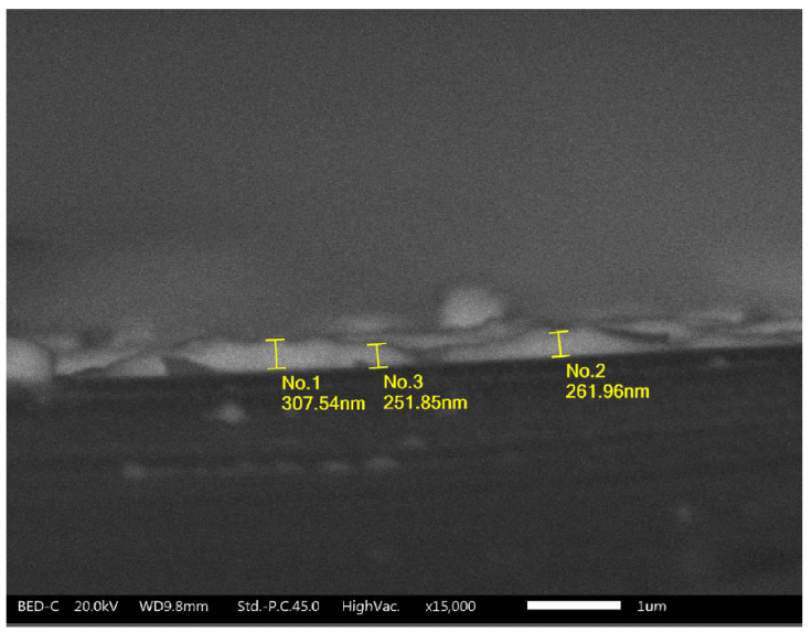
The crystallinity of perovskite thin films was studied by XRD with a Bruker X-ray diffractometer with CuKα radiation (1.5418 Å). The thickness of the perovskite thin films was determined by using a JEOL (JSM-IT300) scanning electron microscope (SEM). The transmission and absorbance spectra were obtained in a Thermo Scientific GENESYS 10S UV-Vis spectrophotometer.
3. Results
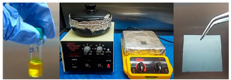
In this section, the results for representative samples arepresented. In Fig. 1, we can see the elaboration process, the yellow solution containing precursors was deposed in one step on the substrate previously heated. After 2 minutes of sintherization a gray color thin film of hybrid perovskite was obtained.
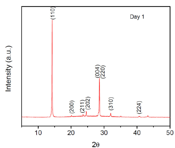
The stability of thin films of CH3NH3Pb0.9Sn0.1I2.5Cl0.2 and CH3NH3Pb0.75Sn0.25I2.5Cl0.5 hybrid perovskites were monitored through XRD and absorbance measurements. Meanwhile, thin films were kept in a Petri dish under environmental conditions. The stable phase of CH3NH3PbI3 normally displays eight diffraction peaks: (110), (200), (211), (202), (004), (220), (310) and (224) corresponding to a tetragonal symmetry [1, 12, 30-33], as we see in Fig. 2.
The diffractogram of non-doped perovskite displays the PbI2 characteristic peak (001) from day 18, whose intensity increases with time indicating a degradation process [23]. The diffractograms obtained for doped perovskites are shown in Fig. 3, where we can see that the hybrid perovskite CH3NH3Pb0.9Sn0.1I2.8Cl0.2 remains almost unchanged until day 35 [Fig. 3a)]. Also, the incipient PbI6 peak is observed with no significant later increase. In contrast, hybrid perovskite CH3NH3Pb0.75Sn0.25I2.5Cl0.5 kept almost unchanged for 20 months, as it is shown in Fig. 3b).
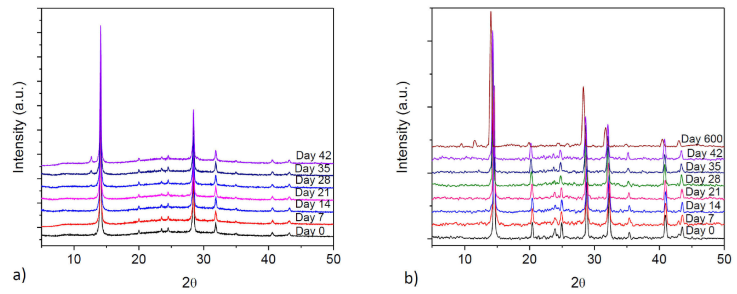
Figure 3 DRX of a) sample of doped perovskite CH3NH3Pb0.9Sn0.1I2.8Cl0.2, no degradation peak is present until 35 days, b) doped perovskite CH3NH3Pb0.75Sn0.25I2.5Cl0.5, showing the degradation peak after 600 days.
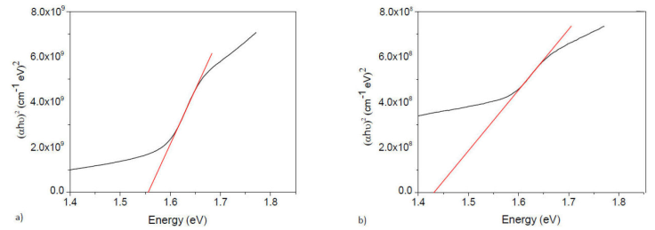
The absorbance spectrum of thin films in the UV-Vis region (400-1100 nm) are showed in Fig. 4. The optical response was monitored until the degradation of hybrid perovskite thin films. An abrupt absorption edge is normally displayed around 780 nm, characteristic of hybrid perovskite [34, 35], which corresponds to the direct gap transition from the first valence band to the conduction band minimum. For doped hybrid perovskites we see the same behavior, indicating that doping does not significantly change the optical properties, [Figs. 4a) and 4b)]. We used the Tauc equation to calculate the optical bandgap value, Eg [25, 26], for a direct bandgap semiconductor:
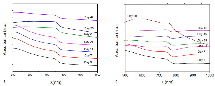
Figure 4 Absorbance versus Energy for a) CH3NH3Pb0.9Sn0.1I2.8Cl0.2 and b) CH3NH3Pb0.75Sn0.25I2.5Cl0.5.
The photon energy, hv, is determined by extrapolation of the linear portion of the curve obtained by plotting (αhv)2 versus hv, until the intercept with the photon energy axis (Fig. 6). The bandgap value is
4. Conclusions
In summary, we have reported the stability improvement of the CH

