


 nueva página del texto (beta)
 Inglés (pdf)
 Artículo en XML
 Referencias del artículo
 Enviar artículo por email
 Citado por SciELO
  Similares en
SciELO
Similares en
SciELO 
 Permalink
1 Introduction
Since the 1990s, inorganic nitrides have attracted the interest of scientists for their chemical and physical properties beneficial for various industrial and technological fields [1]. Inorganic nitrides are divided into two categories according to their electronic properties: semiconductor wurtzite main group metal nitride and superconducting rocksalt transition metal (TM) nitride [2]. The first type such as AlN, GaN et InN present many important characteristics, including direct bandgap, high carrier mobility [1,3], they are largely used in laser diodes, solid states lighting, high data density optical storage media, radio frequency transistors [4, 5]. The second type, such as TiN, VN and NbN, are employed in the hard coating, conduction barriers in semiconductor devices, and superconductors with transitions at a temperature around 20K [6, 7]. Ternary nitride semiconductors are a large class of materials for a wide range of properties because of their unique nature and wide band gaps. Their intermediate bonding character due to the high energy of the nitrogen 2p orbital provides better hybridization with metal orbitals, making semiconductors crucial candidates in optoelectronic and photonic devices [8]. These materials have been widely studied in the past decade [9]. Principle calculations showed that various ternary zinc
nitrides exhibit electronic and optical properties. Using DFT calculations Yoyo Hinuma et al. 2016, investigated the electronic structure, stability and dopability of CaZn2N3 demonstrated tunable direct bandgap, light emission and harvesting. They have also proposed 21 interesting nitride systems, such as Ba2ZnN2 and Zn2PN3[10]. Furthermore, M. Mallmann et al. (2018) have synthesized Mg2PN3 and Zn2PN3 ammonothermally [11] for the first time, and determined bandgap based on diffuse reflectance spectroscopy [12] , which estimated to be 5.0, 3.7 eV for Mg2PN3 and Zn2PN3 respectively. Afterwards, they performed DFT calculation to verify experimental values; both compounds crystallize in wurtzite (WZ)-type superstructure in orthorhombic space group Cmc21[13]. In addition, Zakutayev et al. 2021 have recently synthesized the Zn2NbN3 compound for the first time. Experimental results indicate that Zn2NbN3 crystallizes in cation-disordered WZ-derived cristal structure with 2.1 eV optical band gap and
2 Computational method
The calculations were performed via first-principles fullpotential linearized augmented plane-wave (FP-LAPW) method [16] in the framework DFT calculations as implemented in WIEN2K code [17,
18]. For the exchangecorrelation energy functional, there are two approximations, the local density approximation (LDA) and the generalized gradient approximation (GGA). Realized that the LDA approximation is the most basic non-trivial approximation to the exchange-correlation energy. We assume that the energy XC of the system at a given point is equal to the energy of a homogeneous electron gas with (approximately) the same density at that point. However, we run into problems when describing systems with widely varying electron densities [19,
20]. In our calculation, we used the generalized gradient approximation (GGA) in the Perdew-Burke-Ernzerhof (PBE) form instead of the LDA. Therefore, GGA is a class of functions that consider the density at a given point and the density’s gradient (variation), allowing it to describe systems (to some extent) better. GGA has become a common denominator in many studies, especially when describing large-scale systems with different atoms [21]. In addition, the GGA-PBE approximation provides accurate results for the structural and electronic properties of semiconductors [22,
23]. For the band gap calculations with accuracy, we perform GGA with the addition of Tran-Blaha modified Becke-Johnson (TB-mBJ) exchange potential [22-
25]. The details of the calculations are as follow: The muffin tin radius sphere (
3 Results and discussion
3.1 Structural properties
In our work, we report Zn2NbN3 wurtzite derived orthorhombic structure with Cmc21 (space group 36). In order to obtain the most stable structure, we optimized the structure by calculating different energies for different volumes using GGA-PBE adapting to the Murnaghan equation Eq. (1). The E(V) diagram is shown in Fig. 1b). The stable Zn2NbN3 wurtzite derived orthorhombic crystal with the ordered occupation of Zn and Nb by cationic sites is shown in Fig. 1a) and relaxed lattice parameters are grouped in Table I as well as the previous theoretical and experimental results.
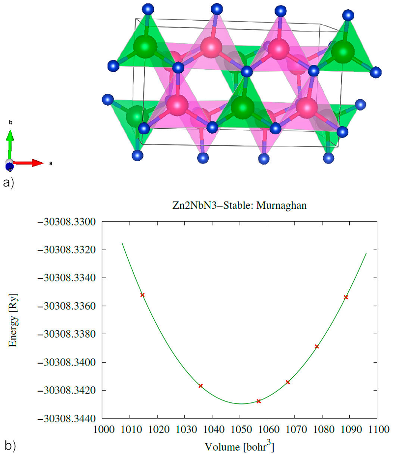
Figure 1 Zn2NbN3 structure optimization a) Zn2NbN3 relaxed structure with atom’s color are Zn (magenta), Nb (green), and N (blue) and b) diagram of energy versus volume.
The thermodynamic stability of Zn2NbN3 was studied by the formation energy, which is described as the difference between the total energy of final products and these of reactants [26, 27]. After relaxation, high-precision static calculations were performed to calculate the precise ground state energies of the reactants and product in order to compute the formation energy per atom of Zn2NbN3 using the following equation:
where
3.2 Electronic properties
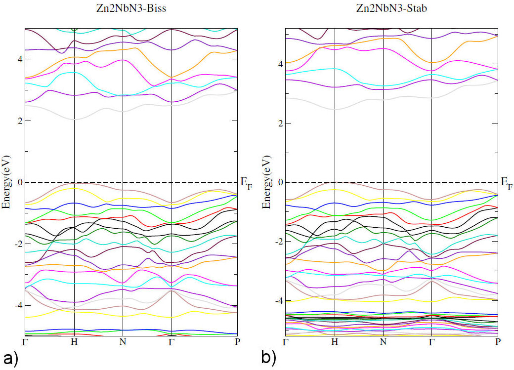
The gap is one of the most important electronic parameters that allow us to get very useful informations about the nature, efficiency, usefulness of the material [22]. The exact bandgap of semiconductors are very appreciable for their efficient use in optoelectronic and other electronic devices, and minimal variation of its value induces significant changes in application devices [28]. In our study’s calculations, the electronic bandgap of Zn2NbN3 is determined using (PBE) and (TB-mBJ). The results are shown in Table II.
Table II Different gaps of Zn2NbN3 compound.
| Gap | PBE | TB-mBJ | Other works [14] |
|---|---|---|---|
| Zn2NbN3 | 2 eV | 2.5 eV | 3.5 - 3.6 eV |
Figure 2 illustrates band structure of Zn2NbN3. We noticed that it is characterized by a direct bandgap with clear semiconducting behavior. Valence band is close to Fermi level, while conduction band do not. We can see that the maximum of valence band and the minimum of conduction band are located at the H point with a value of bandgap about 2 eV and 2.5 eV using (GGA-PBE) and (TB-mBJ) approximations, respectively.
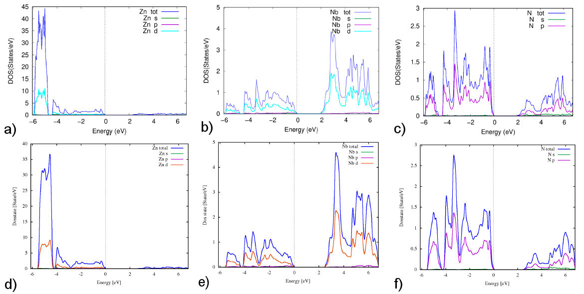
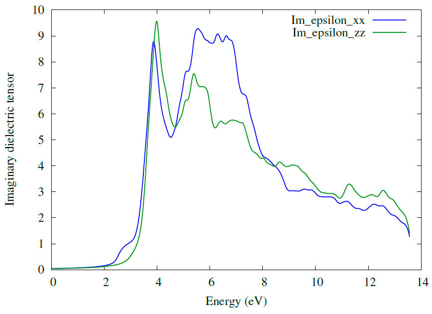
On the other hand, the total density of states (DOS) and the partial DOS play an essential role in investigating the electronic properties of the compounds. In Figs. 3 and 4 show the total DOS and partial DOS of Zn2NbN3 structure and Zn, Nb, and N atoms, respectively, calculated with the two potentials PBE and TB-mBJ. As shown in Fig. 3, the total DOS plot shows a zero-gap at the Fermi level with the two used potentials, confirming the semiconducting behavior in the electronic band structure plot. The total DOS simulated with PBE and TB-mBJ potentials is almost the character of the Zn atom, especially of d orbital in the energy range between -4.5 and -6 eV in the valence band [Fig. 4a) and 4d)]. The energy range -4.5 to 0 eV is dominated by Znd, Nb-d, and N-p orbitals [Figs. 4a) to 4f) respectively], indicating a strong interaction between these atoms. We can also see at the energy interval close to the Fermi level that the main contribution comes from the N-p orbital [Fig. 4c) and 4f)]. In the conduction band, the DFT calculations with the two potentials PBE and TB-mBJ indicate that the main contribution is from Nb-d and N-p orbitals [Figs. 4b), 4c), 4e) and 4f) respectively] with the domination of Nb-d orbital indicating a strong interaction between Nb and N atoms.
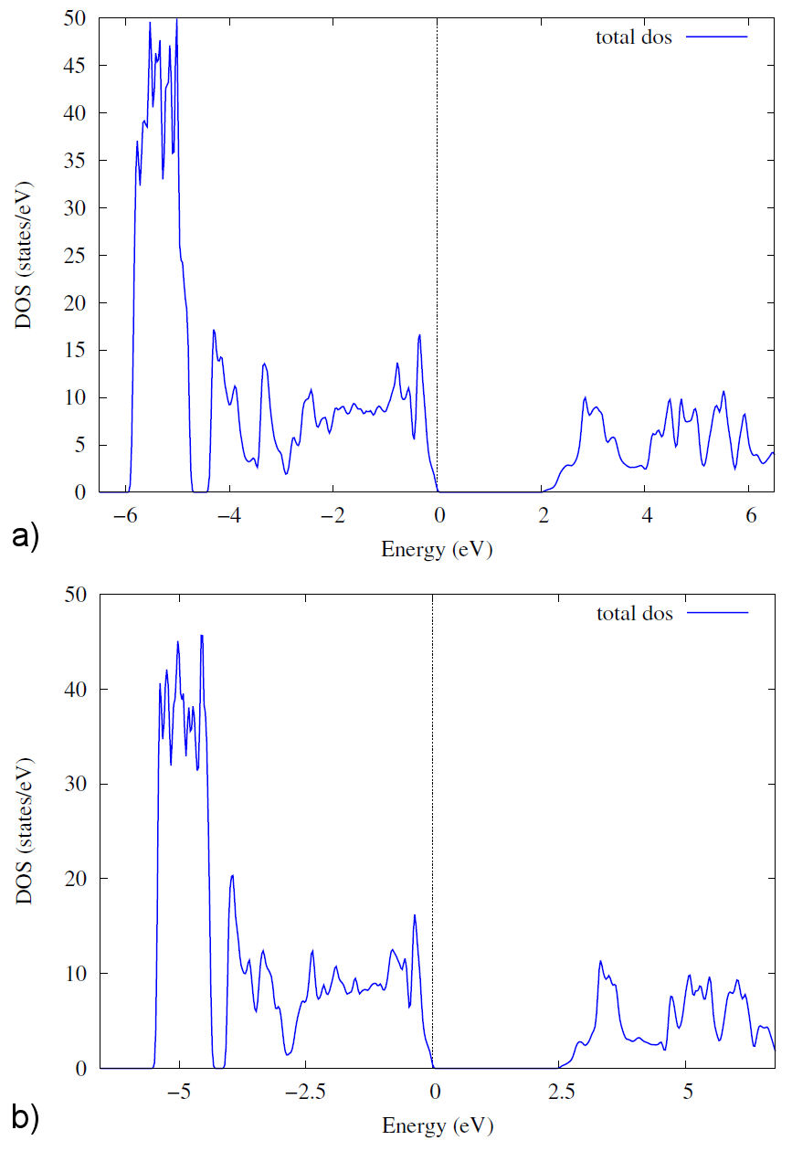
Figure 3 The total density of States of Zn2NbN3 compound with both approximations GGA-PBE and TB-mBJ. a) GGA-PBE approximation, and b) TB-mBJ approximation.
3.3 Optical properties
The optical properties of a material describe its response to electromagnetic radiation. A detailed optical characterization is thus conducted to determine the optoelectronic nature of of Zn2NbN3, using the TB-mBJ approximation and thus support their use in the fabrication of optoelectronic devices.
3.3.1 Dielectric function
The optical properties of any material explain the frequency response to the energy of the incident photon (
where
where
The Kramers-Kronig method can help us to extract the expression of the real part of the dielectric function
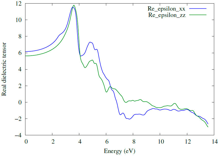
Optical properties were computed using dielectric coefficient values. The real part of the dielectric function shows the ability of a material to respond to the incident electromagnetic wave. The knowledge of both real and imaginary parts of the dielectric function allows the calculation of important optical functions; the static value of real part
3.3.2 Absorption coefficient
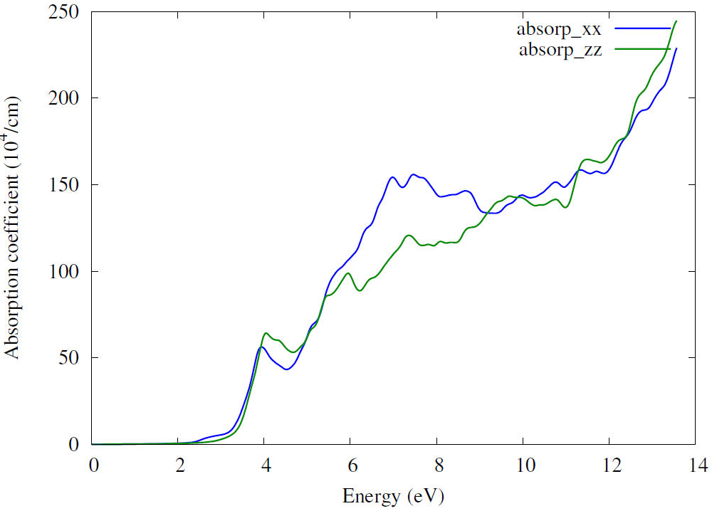
The reason for a transition of an electron from the valence band to the conduction band is the interaction between incident photon and electron, which is related to absorption coefficient [34]. Figure 7 shows spectra of absorption coefficient. Calculations show that our compound possesses transparent behavior below the energy band gap (valance band) because the incident photon’s energy is insufficient to transport electrons from the valance band to the conduction band. The first peak in the plot occurs at 4.04 eV with a value of optical gap estimated to be 3.1 eV. The second appears at 7.3 eV. After that, we notice a growth of the absorption with high energies indicating an effective optical behavior [33]. The appearance of the absorption beyond the energy 3.1 eV means that the absorption in semiconductors occurs when the incident energy exceeds the energy gap. In addition, strong absorption in the ultraviolet region suggests that Zn2NbN3 could be used in UV light protection [35].
3.3.3 Refractive index
Refractive index can be calculated using the relation bellow with the help of real and imaginary part of dielectric function
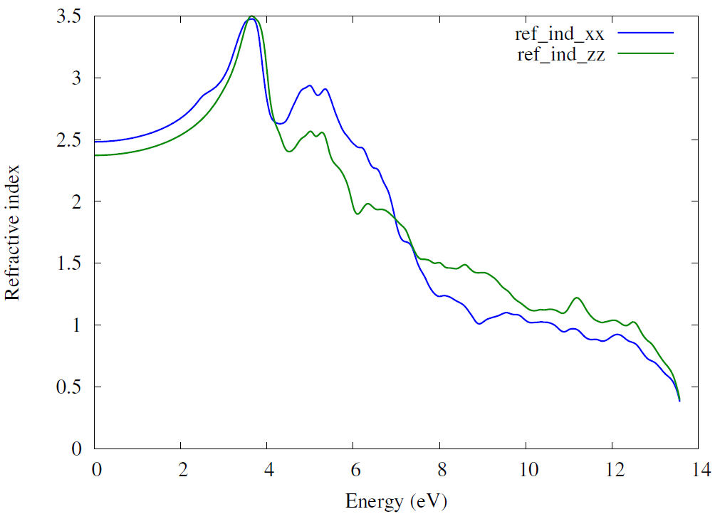
The plot of the refractive index of Zn2NbN3 is shown in Fig. 8, the value of static refractive index
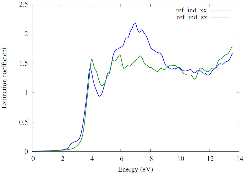
3.3.4 Extinction coefficient
The extinction coefficient shows the amount of radiation absorbed by the material, which explains the similarity between the extinction coefficient and absorption coefficient plots. Extinction coefficient
Figure 9 shows extinction coefficient spectra. We can see the extinction coefficient close to zero in the energy range from 0.0 to 2.0 eV, which means that the electromagnetic wave can completely pass through the material. The first peak is of the order of 1.5, around 4.0 eV. An important peak of 2.2 occurs at 7.0 eV. Hence, the electromagnetic wave passes difficulty through the material after the energy of 2.0 eV.
4 Conclusion
We have computed structural, electronic, and optical properties for Zn2NbN3 by applying DFT theory-based FP-LAPW approach. Structural parameters are a = 9.90 Å and b = 5.81 Å and c = 5.43 Å. The electronic calculations obtained from band structure using both (GGA) and (TB-mBJ) approximations prove direct bandgap and semiconductor behavior. From total and partial DOS performed by employing (GGA) and TB-mBJ approximations, we have concluded that the main contribution is from Nb-d and N-p orbitals, in good agreement with the imaginary part of the dielectric function. The absorption of Zn2NbN3 appears after 3.1 eV, consistent with results from electronic properties, using (PBE) and (TB-mBJ) approximations. The Zn2NbN3 material has a high refractive index and strong optical absorption in the ultraviolet region. So, this compound is suitable for optoelectronic applications.

