


![Theoretical study of [111]-germanium nanowires as anode materials in rechargeable batteries: a density functional theory approach](/img/es/prev.gif)


 nueva página del texto (beta)
 Inglés (pdf)
 Artículo en XML
 Referencias del artículo
 Enviar artículo por email
 Citado por SciELO
  Similares en
SciELO
Similares en
SciELO 
 Permalink
1. Introduction
Two-dimensional systems are a field with a lot of research interest in the last two decades, although these were theoretically reported by P.R. Wallace since 1947 [1] and there are many later works, it was in 2004 when Andre Geim and Konstantin Novoselov mechanically exfoliated a graphene sheet, than gives them the Nobel Prize in 2010 "for groundbreaking experiments regarding the two-dimensional material graphene", that the 2D materials becomes a hight activity research topic. Undoubtedly, the impact of the discovery of 2D systems such as graphene has led to both, theoretical and experimental investigations of a large number of 2D materials such as Silicene, Germanene, and Arsenene [2-4], just to mention some of the most emblematic ones, with a single atom in their constitution, not necessarily in a honeycomb structure.
There are also other hexagonal 2D material with different atoms in the triangular sub-lattice, particularly III-V systems as the gallium nitride (GaN) [5,6], gallium selenide (GaSe) [7] and the gallium arsenide (GaAs), being the former one the system of study in this investigation. In the case of the 2D GaAs I. Rozahun et al. [8] performed a DFT study, using the Cambridge serial total energy package (CASTEP), reporting a relaxed structure with an interatomic distance of 2.409 Å, and its phonon spectra in the real region of frequency, ensuring that the system is stable; they report that the energy gap of the system is 2.568 eV with PBE0 and 1.027 eV with GGA, respectively, as well as a semi-metallic to metallic transitions due to vacancies. The photocatalytic activity of GaAs monolayer computation, by DFT, was investigated in [9] reporting effective mass, stretching modulus, deformation potential, and charge carrier mobility as well as optical absorption in visible region of the electromagnetic spectrum. H. Mishra and S. Bhattacharya [10] computed nonlinear optical properties on buckled GaAs monolayer using quantum espresso package, particularly the second and third harmonic generation, reporting an interatomic distance of 2.338 Å, and a bandgap of 1.13 eV and 2.95 eV for DFT and G0W0, respectively. Just to mention other recent work A. González-García et al. [11] do an ab initio study for 2D hydrogenated gallium arsenide. An important DFT calculations review of group IV and III-V honeycomb structures is reported by Şahin et al. [4], and other deformed octagon-hexagon-square structures of IV and V elements and III-V compounds is reported by T. Gorkan et al. [12]. Finally, some other configurations as GaAs/BN heterostructures [13], GaAs/SiH van der Waals type-II heterostructure [14], graphene/GaAs heterostructure [15], as well as GaAs clusters [16,17] has been recently reported in the literature.
So, the 2D GaAs is an interesting, and novel system for several applications as clearly stated in the previous paragraph, that deserves to be investigated in this paper using the density functional theory (DFT), computing band structure, density of states as well as the imaginary part of the dielectric. The aim of this study is to investigate the very basic physical properties for a freestanding 2D GaAs sheet, as well as the effect of silicon (Si) substitutional atoms on the reported properties, since it has an amphoteric nature in the GaAs, meaning that depending on which atom is substituted, this can be an n- or p-type impurity atom. We will report, as expected, that the impurity levels do indeed appear near the conduction band (or valence), if the impurity is n-type (or p-type), respectively. Also the density of states due to the impurity is modified and as well as the imaginary part of the dielectric function.
The organization of the paper is the following: in Sec. 2, we introduce used the implemented DFT method and and the computational details, in Sec. 3, we present the results and make de discussion, and finally the conclusions are given in Sec. 4.
2. Computational details
The computational study of this 2D nanostructured material was carried out under the density functional theory (DFT), using the Spanish Initiative for Electronic Simulation with Thousands of Atoms (SIESTA) code, that implemented a Linear Combination of Atomic Orbitals (LCAO) basis set, and is a method and computational program for ground state electronic and optical properties reported by José M. Soler et al. [18], and its recently developments has been reported in [19] by the SIESTA group. For the calculations of geometry and electronic structure, the correlation and exchange energy are treated in the generalized gradient approximation (GGA), according to the Perdew-Burke-Ernzerhof (PBE) parameterization [20], considering a double ζ-polarized basis set.
We performed an initial relaxation, with 3 × 3 × 1 Monkhorst-Pack k-points, a 300 Ry mesh-cutoff parameter and a maximum force tolerance of 0.04 eV/Ang. After this we do a total energy convergency procedure, to determine Monkhorst-Pack k-points and mesh-cutoff parameter, and then we do a second relaxation procedure with a maximum force tolerance of 0.01 eV/Ang. We compute the band structure and density of states (DOS), as well as the imaginary part of the dielectric function for a pristine 2D GaAs, with two atoms in the unit cell. After that, to consider impurities, we construct a 5 × 5 supercell that consist of 50 atoms, to do substitutional impurities of silicon in a gallium position (n-type) and in an arsenic site (p-type). In the next section we present the obtained results and we give more information of the used parameters in each section.
3. Results and discussion
Here, we first will present the results for the pristine 2D GaAs freestanding sheet, reporting the band structure, the density of states and the imaginary part for the dielectric function. Then we do the same considering one silicon substitutional atom in gallium position (n-type) and one silicon substitutional atom in arsenide position (p-type) in the 50 atoms supercell.
3.1. Pristine 2D GaAs
In Fig. 1, we present the relaxed structure for the pristine 2D GaAs with 500 Ry mesh-cutoff parameter and 31 × 31 × 1 Monkhorst-Pack special k-points [21], that ensures the total energy convergence. The considered maximum force tolerance in the conjugate gradients (CG) relaxation method is 0.01 eV/Å, giving a relaxed interatomic Ga-As distance of 2.559 Å, that is little bit bigger than the reported by H. Mishra and coworker [10]. With the relaxed structure we compute the band structure for the system following the Γ - M - K - Γ especial k-points path in the Brillouin zone considering 100 points between each k-point. Then we do the density of states (DOS) determination, with 501 × 501 × 1 k-points grid in the PDOS Monkhorst-Pack block, that ensures a well defined DOS for the structure. The band structure and DOS for the pristine 2D GaAs is depicted in Fig. 2, where we obtain a direct band gap material with an energy gap of 0.824 eV, lower than the reported by other authors that is a well known issue in DFT computations, but the band structure and the DOS structure are in good agreement with previous results [8,10].
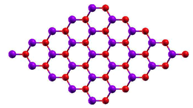
Figure 1 Relaxed structure for pristine 2D GaAs. In this figure we represent the gallium atoms in red and the arsenide ones in blue.
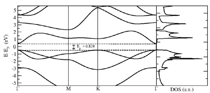
Figure 2 Band structure with Γ - M - K - Γ path, with the corresponding density of states of pristine 2D GaAs.
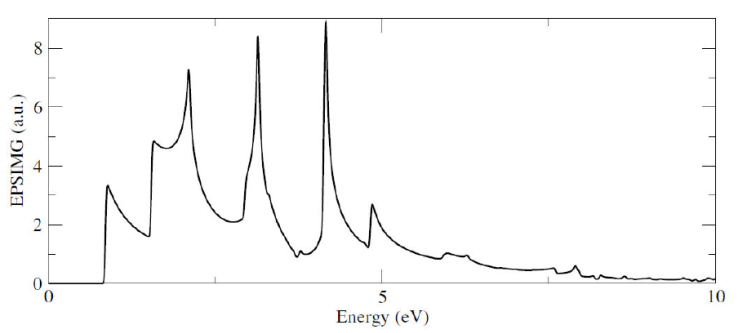
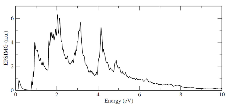
Finally, we do compute the imaginary part of the dielectric function
3.2. A silicon atom in a gallium position.
Now, we will discuss the effect of consider silicon, that is a group IV atom, in a gallium position, that has tree valence electrons, in such a way that we are introducing a n-type impurity atom and we will study the effect on the structure, bands and density of states as well as in the imaginary part of the dielectric function.
In this section, we take into account one substitutional silicon (yellow atom) in a gallium position (red atom), labeled here as 1Si-Ga. For this to be possible we use the supercell method, in such a way that we do a 5 × 5 supercell, that consist of 50 atoms, and put a Si atom in an arbitrary Ga position. In Fig. 4, we show the relaxed structure, with a maximum force tolerance of 0.01 eV/Å, for the system; from Fig. 4a), z viewpoint of figure, we can see that the hexagonal structure is kept but the interatomic distance between the Si atom with As neighborhood atoms (blue ones) is now 2.45 Å, lower that the one for the GaAs interatomic distance in the pristine 2D GaAs, due to coulombian forces, that induces a local deformation. In fact, from Figs. 4b) and c), that are the x and y side-views, we can observe that the Si atom deviates from the original Ga position, after relaxation, and locally deformed the system.
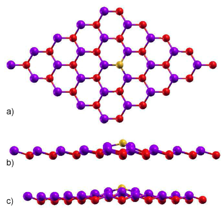
Figure 4 Relaxed structure for a substitutional silicon atom in a Ga position, 1Si-Ga. The gallium atom is the red one, while the arsenic one is blue. The a) z, b) x, and c) y views are depicted.
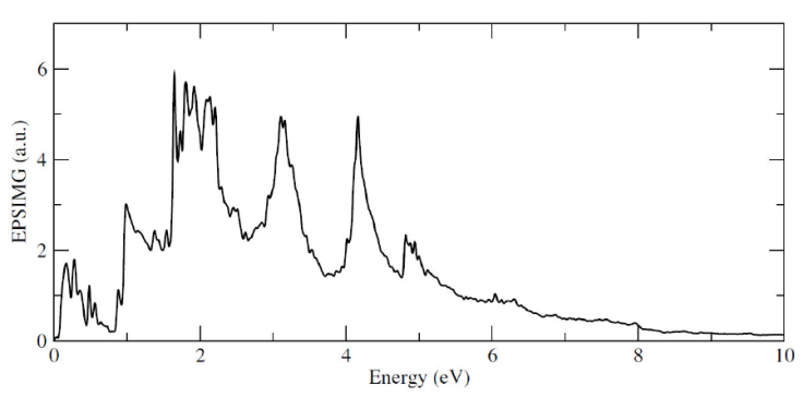
Figure 5 show the band structure and the density of states for the 1Si-Ga system. Here, we can observe that effectively, an energy level appears close to the conduction band minimum, labeled with a red line, and that it has a well defined peak in the DOS. On the other hand, in Fig. 6 the imaginary part of the dielectric function for the system is shown, and we can see that the presence of this n-type impurity, in comparison with the pristine case, induces a more rich peak structure but even must important, an asymmetric gaussian like structure near the zero of energy. This is important because the presence of this substitutional atom modify the optical behavior of the system, with optical response in the visible region on the electromagnetic spectrum.
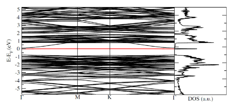
Figure 5 Band structure with Γ - M - K - Γ path, with the corresponding density of states for the 1Si-Ga system.
3.3. A silicon atom in an arsenic position
Just for the amphoteric nature of the silicon atom, now we consider the group IV silicon atom in an arsenic position, that has five valence electrons, in such a way that we are introducing now a p-type impurity atom and will discuss the effect on the reported properties.
Figure 7 shows the relaxed structure for the 1Si-As situation and, as in the previous discussion, the system experiences a small local deformation as can clearly seen from this figure, but now the interatomic distance of Si atoms with the first Ga neighborhoods is 2.512 Å, that is closer than those reported for the pristine case, that is why it did not affect too much the relaxed structure, as in the previous case. This is an important fact to stress, because it means that depending on the position adopted by the silicon atom, this can importantly affect the structure (n-type impurity) or not too much (p-type one).
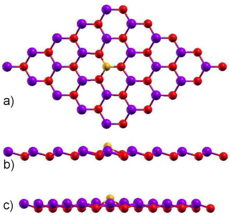
Figure 7 Relaxed structure for a substitutional silicon atom in an arsenic position, 1Si-As. The gallium atom is the red one, while the arsenide is blue. The a) z, b) x, and c) y views are depicted.
Finally, in Figs. 8 and 9 we present band structure with the correspondingly DOS and the imaginary part of the dielectric function for the 1Si-As configuration, respectively. Once again, as expected, it appears an energy level close to the valence band maximum at the Fermi level, the characteristic one for p-type impurities, and its corresponding well defined peak in the DOS; in the imaginary part for the dielectric function, from which all the optical responses can be computed with the Kramers-Kronig relations, has an important peak structure, particularly in the optical region of the electromagnetic spectrum.
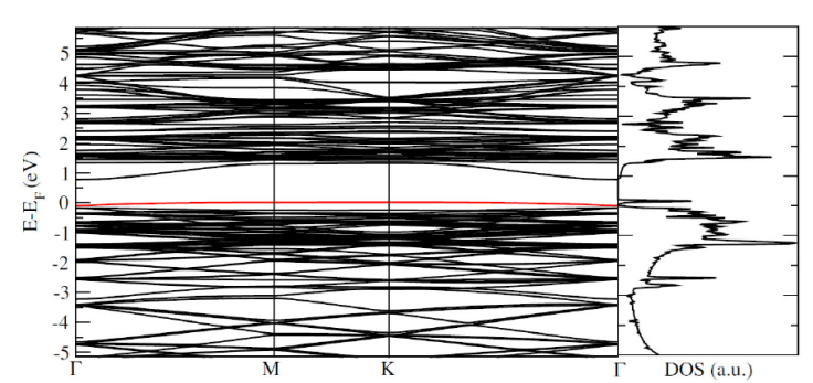
Figure 8 Band structure with Γ - M - K - Γ path, with the corresponding density of states for the 1Si-As system.
4. Conclusions
In summary, in this paper we report the band structure and the density of states for a pristine 2D GaAs within the framework of density functional theory (DFT), using the SIESTA code, reporting direct optical transition with an energy gap of 0.824 eV, we also report the DOS and imaginary part of the dielectric function in good agreement with previous results, less the energy gap values, a common result in DFT computations. We also report, for the first time, the band structure and the density of states considering n-type impurities (1Si-Ga) and p-type ones (1Si-As) in the 2D GaAs obtaining, as expected, an energy level close to the conduction band minimum, and the corresponding one is found close to the valence band maximum, respectively. The imaginary part of the dielectric function reflect the effect of the silicon impurities that will allow modification in the optical response functions by means of the Kramers-Kronig relations, but at this stage conclude that the silicon acts as an amphoteric impurity as does in the bulk GaAs and it will affect the electronic and optical response.

