


 nueva página del texto (beta)
 Inglés (pdf)
 Artículo en XML
 Referencias del artículo
 Enviar artículo por email
 Citado por SciELO
  Similares en
SciELO
Similares en
SciELO 
 Permalink
1. Introduction
Transparent conductive oxides (TCOs), one of the best choices as the material used in optoelectronic devices such as flat panel displays, photovoltaic cells, smart windows, surface acoustic wave devices, light-emitting diodes, and optical waveguides [1,3], has many TCOs such as Tin oxide (SnO2) [2], zinc oxide (ZnO) [4], cadmium oxide (CdO) [5]. CdO (cadmium oxide) thin films have sparked substantial attention in recent years because of their numerous advantages such as growth conditions, shape, size, direct and wide bandgap. surface thickness control, low resistivity, and chemical stability [6]. CdO is a group II-VI transparent conductor with a direct bandgap of 2.3 - 2.7eV and an n-type conductivity with crystallites that are simple cubic crystal systems with an Fm-3m space group and a lattice constant of 4.67Å [7]. Furthermore, a relatively low electrical resistivity of 10-3 to 10-4Ωcm was used in many optoelectronic applications such as transparent conducting oxides, solar cells, smart windows, optical communications, flat-panel displays, phototransistors, and other types of applications such as IR heat mirrors, gas sensors [8,9,10].
Many processes may be used to obtain un-doped, doped CdO thin films including pulsed laser deposition [11], thermal evaporation[12], sputtering [13], sol-gel [14], Metallo-organic chemical vapor deposition (MOCVD) [15], electro-spinning[16], and spray pyrolysis [17]. Among these approaches, spray pyrolysis remains appealing and interesting due to its low cost, simplicity, speed, and ability to create large-area coatings.
It has been shown, according to the literature, that the physical properties of CdO thin films can be improved by introducing an appropriate dopant with a covalent radius less than or to that of the host lattice atoms. On the on the other hand, it could be interesting to explore the incorporation of two types of dopant elements instead of one to examine their effects on the CdO films properties.
In the present work, the prepared
2. Experimental details
The Transition Metal
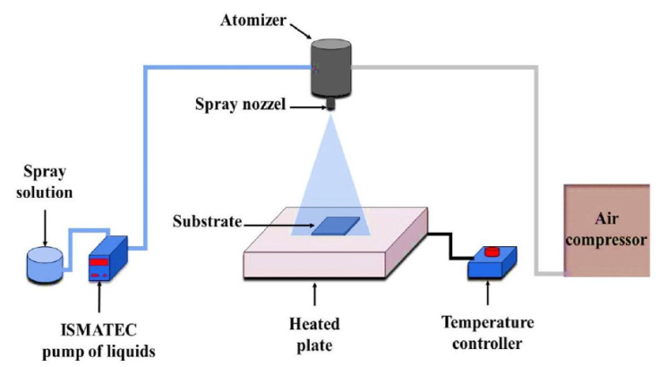
Table I Deposition conditions of the obtained thin films.
| Chemical precursors | Cadmium acetate |
|---|---|
| (Cd (CH3(COO)2.2H2O) | |
| Deposit temperature | 350 ± 10°C |
| Distance between atomizer and hotplate | 27 cm |
| Spray solution flow rate | 1 ml/min |
| volume of sprayed solution | 10 ml |
3. Results and discussion
3.1. Structural properties
The structural characterization was performed at room temperature using a Bruker X-ray diffractometer model D2 Phaser with CuKα radiation λ = 1.5406 Å.
Figure 2 shows the XRD patterns of the deposited thin films. It reveals that the diffracted peaks located at
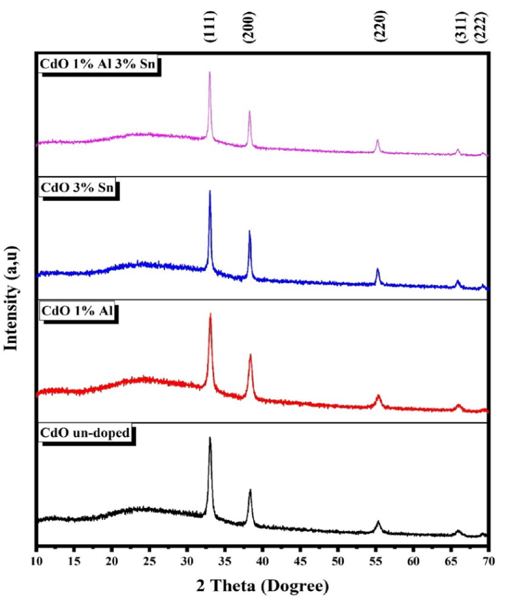
From Fig. 2, we notice that the intensity of peak (111) increases slightly after doping, which could be attributed to the dopant incorporations into the CdO matrix of our obtained films. This behavior has been, already, observed in literature [8,20]. The average crystallites size of the films was calculated using the Scherrer formula [21].
where D is the crystallite size, λ(1.5406 Å), β is the FWHM (Full Width Half Maximum) in radians of the peak (111) and θ is the Braggs angle. From the Table III, it is seen that the crystallite size increased with Sn doped and Al-Sn co-doping.
The constant lattice a, strain ε, and dislocation density δ for CdO films determined using the following relationships [22,23].
As shown in Table III, the crystallite size of the CdO films decreased with 1% Al doping. This decrease could be attributed to the strained crystal growth due the Al incorporation [24]. On the other hand, the crystallite size TCO and ATCO thin films increased with tin and aluminium incorporation which explains the improvement of the crystallinity of the films. The value of the lattice parameter of the CdO obtained films decreases with Al and Sn doping and increases with the Al-Sn co-doping. This change tendency of the lattice parameter value with doping and co-doping could be explained the substitution of Cd2+ ions with Al3+ and Sn4+ ones in CdO matrix as well as the Al and Sn atom migrating in the grain boundaries [25].
3.2. Optical properties
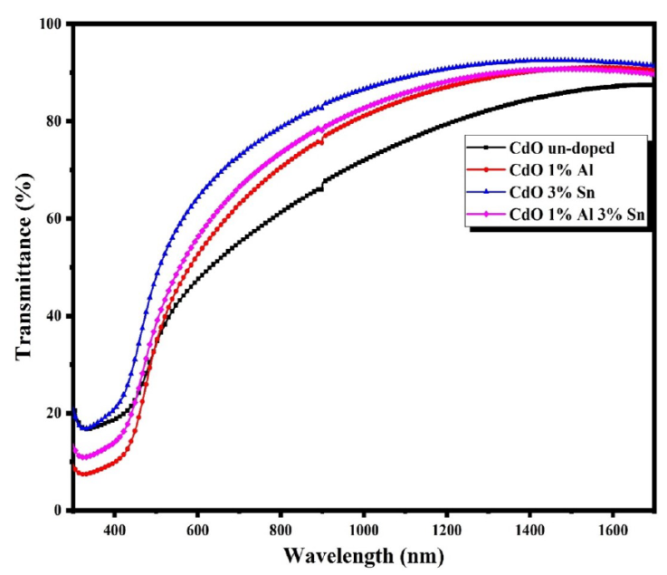
The optical transmittances were recorded using a JASCO 570 type UVvisible-NIR double-beam spectrophotometer.
Figure 3 shows the optical transmittances in the wavelength range of 300-1700 nm of the prepared thin films. An average transmission of 61-79% has been observed in the visible region. The optical transparency of the films has been clearly increased and reached a maximum value around 79% for TCO thin films. This optical transparency improvement could be explained by the crystallinity enhancement of the TCO films (Table III). It is well known that changes in transmittance values depend on the characteristics of the materials, such as crystalline quality, surface morphology, and free carrier concentrations in films [18].
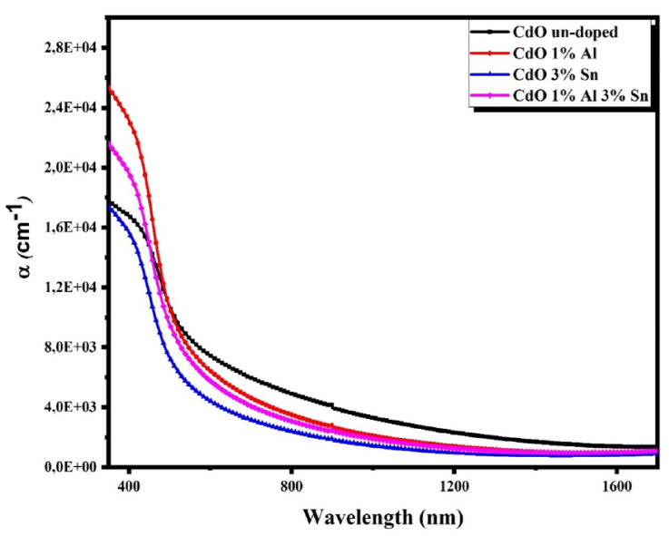
The variations curves of the absorption coefficient
where T is the transmittance and t is the film thickness. The evolutions of the absorption coefficients with wavelength for the obtained thin films are shown in Fig. 4. This figure shows that α values are in the order of 10+4 cm-1 which is in good agreement with literature [26]. The optical band gaps of the obtained films were determined with Tauc relation [27].
where α is the absorption coefficient, hv the photon energy, A constant and Eg the optical band gap. We take n = 2 for direct band gap semiconductor.
The band gap value of un-doped CdO films is estimated as 2.29 eV which agrees with the literatures [6]. The optical gap increased from 2.29 eV for CdO films to 2.49 for TCO (Fig. 5), this increase could be explained by the contribution of the Moss-Burstein effect [28,29].
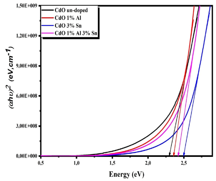
The Urbach energy Eu was estimated by using the following expression [30]
where a 0 is a constant and Eu the Urbach energy. The values of Eu are determined from the reciprocal of the slope of the relation between In a and hv, and the obtained results are summarized in Table IV. We observe that Eu values change inversely with direct optical band gaps for the co-doped films, confirming the minimization of defect states in the prepared films [31].
3.3. Morphological and EDX
The surface morphology and the chemical composition analyses were carried out using a Jeol JSM 5800 scanning electron microscope which is equipped with an energy dispersive X-ray detector (EDX, IXRF Model 550i). The surface morphologies of the obtained thin films are presented in Fig. 6. This figure indicated that the deposited films are dense and no cracks are observed on large scan area. The chemical composition checking by the EDX spectra, is given in the Fig. 7. EDX spectra shown the presence of Cd, Sn, Al and O in the obtained thin films, the presence of Si (the most intense peak) is due to the substrate effect. The reported EDX data confirms the previous XRD analysis. The chemical compositions in percentage are summarized in Table VI.
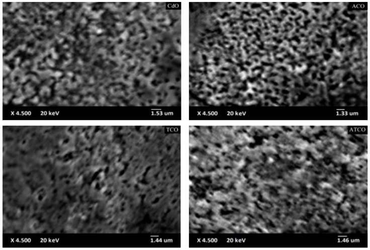
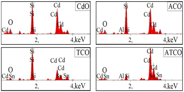
Table V Element concentrations in CdO, ACO, TCO and ATCO thin films.
| Concentration at. % | |||||
|---|---|---|---|---|---|
| Cd | O | Si | Al | Sn | |
| CdO | 31.64 | 38.71 | 29.65 | - | - |
| ACO | 31.34 | 35.25 | 31.98 | 1.43 | - |
| TCO | 30.17 | 35.16 | 33.07 | - | 1.60 |
| ATCO | 54.06 | 30.48 | 10.50 | 2.06 | 2.90 |
3.4. Electrical properties
The electrical properties were performed by ECOPIA HMS-5000 Hall Effect measurement system at room temperature. The carrier concentration n, mobility μ and resistivity ρ of the obtained films are presented in Table VI. The negative sign of the Hall coefficient confirms the n-type conductivity of our films which is in agreement with literatures [32]. The carrier concentrations are in the order of 10+20 cm-3. The resistivity of the obtained films decreased from 1.85 × 10⁻³ Ωcm for un-doped CdO films to 7.85 × 10⁻⁴ Ωcm for ACO films which is attributed to the increases in mobility and decrease in sheet resistance. The resistivity decreasing of the CdO films with Al incorporation has been already reported in literature [32].
4. Conclusion
In this work, the XRD results demonstrate that all the films have a cubic structure with an orientation plane (111). The obtained samples are transparent in the visible region with an average of transmittance value which could be increased from 61 % to 79 % with Sn doping. The optical band gap Broadening from 2.29 to 2.49 eV could be attributed to the BursteinMoss effect. The resistivity value minimum was observed for the ACO samples (7.85 × 10⁻⁴ Ωcm). The results presented in this study showed that Sn and/or Al incorporation in CdO thin films improve their physical properties films.

