<?xml version="1.0" encoding="ISO-8859-1"?><article xmlns:mml="http://www.w3.org/1998/Math/MathML" xmlns:xlink="http://www.w3.org/1999/xlink" xmlns:xsi="http://www.w3.org/2001/XMLSchema-instance">
<front>
<journal-meta>
<journal-id>1665-3521</journal-id>
<journal-title><![CDATA[Superficies y vacío]]></journal-title>
<abbrev-journal-title><![CDATA[Superf. vacío]]></abbrev-journal-title>
<issn>1665-3521</issn>
<publisher>
<publisher-name><![CDATA[Sociedad Mexicana de Ciencia y Tecnología de Superficies y Materiales A.C.]]></publisher-name>
</publisher>
</journal-meta>
<article-meta>
<article-id>S1665-35212014000100001</article-id>
<title-group>
<article-title xml:lang="en"><![CDATA[Memristance effect of metal-insulator-metal structures using Al2O3 film as active layer for emergent memory devices]]></article-title>
</title-group>
<contrib-group>
<contrib contrib-type="author">
<name>
<surname><![CDATA[Molina]]></surname>
<given-names><![CDATA[J.]]></given-names>
</name>
<xref ref-type="aff" rid="A01"/>
</contrib>
<contrib contrib-type="author">
<name>
<surname><![CDATA[Valderrama]]></surname>
<given-names><![CDATA[R.]]></given-names>
</name>
<xref ref-type="aff" rid="A01"/>
</contrib>
<contrib contrib-type="author">
<name>
<surname><![CDATA[Calleja]]></surname>
<given-names><![CDATA[W.]]></given-names>
</name>
<xref ref-type="aff" rid="A01"/>
</contrib>
<contrib contrib-type="author">
<name>
<surname><![CDATA[Rosales]]></surname>
<given-names><![CDATA[P.]]></given-names>
</name>
<xref ref-type="aff" rid="A01"/>
</contrib>
<contrib contrib-type="author">
<name>
<surname><![CDATA[Zúñiga]]></surname>
<given-names><![CDATA[C.]]></given-names>
</name>
<xref ref-type="aff" rid="A01"/>
</contrib>
<contrib contrib-type="author">
<name>
<surname><![CDATA[Gutiérrez]]></surname>
<given-names><![CDATA[E.]]></given-names>
</name>
<xref ref-type="aff" rid="A01"/>
</contrib>
<contrib contrib-type="author">
<name>
<surname><![CDATA[Hidalga]]></surname>
<given-names><![CDATA[J.]]></given-names>
</name>
<xref ref-type="aff" rid="A01"/>
</contrib>
<contrib contrib-type="author">
<name>
<surname><![CDATA[Torres]]></surname>
<given-names><![CDATA[A.]]></given-names>
</name>
<xref ref-type="aff" rid="A01"/>
</contrib>
</contrib-group>
<aff id="A01">
<institution><![CDATA[,National Institute of Astrophysics, Optics and Electronics  ]]></institution>
<addr-line><![CDATA[ Puebla]]></addr-line>
<country>Mexico</country>
</aff>
<pub-date pub-type="pub">
<day>00</day>
<month>00</month>
<year>2014</year>
</pub-date>
<pub-date pub-type="epub">
<day>00</day>
<month>00</month>
<year>2014</year>
</pub-date>
<volume>27</volume>
<numero>1</numero>
<fpage>1</fpage>
<lpage>6</lpage>
<copyright-statement/>
<copyright-year/>
<self-uri xlink:href="http://www.scielo.org.mx/scielo.php?script=sci_arttext&amp;pid=S1665-35212014000100001&amp;lng=en&amp;nrm=iso"></self-uri><self-uri xlink:href="http://www.scielo.org.mx/scielo.php?script=sci_abstract&amp;pid=S1665-35212014000100001&amp;lng=en&amp;nrm=iso"></self-uri><self-uri xlink:href="http://www.scielo.org.mx/scielo.php?script=sci_pdf&amp;pid=S1665-35212014000100001&amp;lng=en&amp;nrm=iso"></self-uri><abstract abstract-type="short" xml:lang="en"><p><![CDATA[The memristor effect (cyclic switching from a High-Resistance State to a Low-Resistance State and viceversa) and a conductivity/resistivity window (I OFF/I ON ratio) of more than 4 orders of magnitude have been obtained in Metal-Insulator-Metal (MIM) structures that use Al2O3 as oxide layer after cyclic I-V measurements. Before initial breakdown, different carrier conduction properties are found when using whether a highly reactive or a highly inert metal as the bottom electrode of the memory structure. These carrier conduction properties for the MIM structure are also affected by changing the deposition conditions of the bottom electrode (by changing the average roughness of its surface) or by using different Al2O3 thickness. Most importantly, because of the low thermal budget used for fabrication of these devices (only 300°C), they have the potential to be vertically integrated as memory cells in higher metallization levels of a CMOS-based Back-End-Of-Line (BEOL) processing. This is important since it would promote real 3-D integration of memory devices for advanced circuit manufacturing.]]></p></abstract>
<kwd-group>
<kwd lng="en"><![CDATA[Memristance Effect]]></kwd>
<kwd lng="en"><![CDATA[MIM structures]]></kwd>
<kwd lng="en"><![CDATA[Atomic-Layer Deposition]]></kwd>
<kwd lng="en"><![CDATA[Al2O3]]></kwd>
<kwd lng="en"><![CDATA[BEOL Processing]]></kwd>
<kwd lng="en"><![CDATA[Conduction Mechanisms]]></kwd>
<kwd lng="en"><![CDATA[RRAM Devices]]></kwd>
</kwd-group>
</article-meta>
</front><body><![CDATA[  	    <p align="center"><font face="verdana" size="4"><b>Memristance effect of metal&#45;insulator&#45;metal structures using Al<sub>2</sub>O<sub>3</sub> film as active layer for</b> <b>emergent memory devices</b></font></p>  	    <p>&nbsp;</p>  	    <p align="center"><font face="verdana" size="2"><b>Molina J.*, Valderrama R., Calleja W., Rosales P., Z&uacute;&ntilde;iga C., Guti&eacute;rrez E., Hidalga J., Torres A.</b></font></p>  	    <p>&nbsp;</p>  	    <p align="justify"><font face="verdana" size="2"><i>National Institute of Astrophysics, Optics and Electronics, INAOE Luis Enrique Erro # 1, Tonantzintla, Puebla, 72000. Mexico.</i> <i>*</i> <a href="mailto:jmolina@inaoep.mx">jmolina@inaoep.mx</a></font></p>  	    <p>&nbsp;</p>  	    <p align="justify"><font face="verdana" size="2">Recibido: 2 de septiembre de 2013    <br> 	Aceptado: 29 de diciembre de 2014.</font></p>  	    <p>&nbsp;</p>  	    ]]></body>
<body><![CDATA[<p align="justify"><font face="verdana" size="2"><b>Abstract</b></font></p>  	    <p align="justify"><font face="verdana" size="2">The <i>memristor effect</i> (cyclic switching from a High&#45;Resistance State to a Low&#45;Resistance State and viceversa) and a conductivity/resistivity window (I<sub>OFF</sub>/I<sub>ON</sub> ratio) of more than 4 orders of magnitude have been obtained in Metal&#45;Insulator&#45;Metal (MIM) structures that use Al<sub>2</sub>O<sub>3</sub> as oxide layer after cyclic I&#45;V measurements. Before initial breakdown, different carrier conduction properties are found when using whether a highly reactive or a highly inert metal as the bottom electrode of the memory structure. These carrier conduction properties for the MIM structure are also affected by changing the deposition conditions of the bottom electrode (by changing the average roughness of its surface) or by using different Al<sub>2</sub>O<sub>3</sub> thickness. Most importantly, because of the low thermal budget used for fabrication of these devices (only 300&deg;C), they have the potential to be vertically integrated as memory cells in higher metallization levels of a CMOS&#45;based Back&#45;End&#45;Of&#45;Line (BEOL) processing. This is important since it would promote real 3&#45;D integration of memory devices for advanced circuit manufacturing.</font></p>  	    <p align="justify"><font face="verdana" size="2"><b>Keywords:</b> Memristance Effect; MIM structures; Atomic&#45;Layer Deposition; Al<sub>2</sub>O<sub>3;</sub> BEOL Processing; Conduction Mechanisms, RRAM Devices.</font></p>  	    <p>&nbsp;</p>  	    <p align="justify"><font face="verdana" size="2"><b>1 Introduction</b></font></p>  	    <p align="justify"><font face="verdana" size="2">Resistive&#45;switching Random Access Memory (RRAM) devices have attracted considerable attention in recent years for their superior characteristics, including their simple memory structure which is usually composed of Metal&#45;Insulator&#45;Metal (MIM) stacks, deep scalability, ultra&#45;low power consumption, fast write/erase speed, and long retention times &#91;1&#45;4&#93;. For RRAM devices, metal oxides based on high dielectric constant materials <i>(high&#45;k)</i> are widely used because of their resistive switching properties and their general physical characteristics which make them compatible with a silicon CMOS&#45;BEOL fabrication process &#91;2&#45;4&#93;. However, several improvements are still needed before RRAM devices become attractive to the semiconductor industry: higher endurance cycles, adequate write/erase margins, multi&#45;level resistance storage and most importantly, understanding and correlating the precise mechanisms required for resistive switching o their fabrication process conditions.</font></p>  	    <p align="justify"><font face="verdana" size="2">A better understanding of the physics related to resistive switching will be helpful in achieving these goals. Even though it is widely recognized that resistive switching mainly originates from the forming/rupture of ultra&#45;thin conductive filaments in the oxide film, the precise physics and chemistry of this switching behavior is ambiguous and remains fully unanswered. Ideally, RRAM switching modes can be classified in two groups: <i>unipolar switching,</i> which means the resistive switching depends on the amplitude of the applied voltage but not on the polarity; and <i>bipolar switching,</i> which means the resistive switching relies on the polarity of the applied voltage bias &#91;5&#93;. During switching, the memory resistance states can be changed from a High Resistance State (HRS) to a Low Resistance State (LRS) by SET and RESET voltage pulses respectively.</font></p>  	    <p align="justify"><font face="verdana" size="2">In an effort to better understand the RRAM's switching phenomena, we present the electrical characteristics of MIM structures varying some parameters in their fabrication process as well as using different materials as bottom electrode; all to assess the conduction mechanisms of carriers just before the initial switching occurs.</font></p>  	    <p>&nbsp;</p>  	    <p align="justify"><font face="verdana" size="2"><b>2 Experimental Procedures
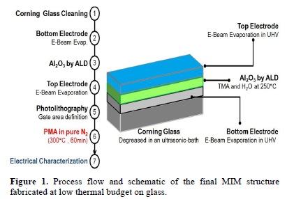
</b></font></p>  	    ]]></body>
<body><![CDATA[<p align="justify"><font face="verdana" size="2">For all samples, glass slides were used as substrates which were cleaned by sequential ultrasonic cleanings in acetone, methanol, and iso&#45;propanol; then all the substrates were rinsed with deionized water and dried with pure nitrogen flow. Two different MIM structures were obtained: Al/Al<sub>2</sub>O<sub>3</sub>/Al and Al/Al<sub>2</sub>O<sub>3</sub>/W stacks. First, aluminum (400 nm in thickness) was used as bottom electrode in an initial set of samples. Tungsten (500 nm in thickness) was used as bottom electrode in another set. Both metals for the bottom electrode were deposited by E&#45;beam evaporation under ultra&#45;high vacuum conditions. Then, Al<sub>2</sub>O<sub>3</sub> was deposited directly on the bottom electrode by Atomic&#45;Layer Deposition (ALD, Savannah&#45;S100 system from Cambridge&#45;Nanotech) using H<sub>2</sub>O and Trimethyl&#45;Aluminum (TMA) as precursor gases. At a growth temperature of 250&deg;C, an average Al<sub>2</sub>O<sub>3</sub> thickness of 10nm and 20nm were obtained. Finally, aluminum was used as top electrode for all structures (500 nm in thickness) and it was deposited by E&#45;beam evaporation directly on Al<sub>2</sub>O<sub>3</sub>. After MIM fabrication and lithography process (for gate pattern definition), a thermal treatment in N<sub>2</sub> (99.999% purity) at 300&deg;C was applied to all samples and this was the maximum processing temperature used during fabrication of these structures. The area for all devices is 64e<sup>&#45;6</sup> cm<sup>2</sup>.</font></p>  	    <p align="justify"><font face="verdana" size="2">All samples were electrically characterized using a Keihtley Model 82&#45;DOS Simultaneous C&#45;V system in order to obtain the dielectric constant and capacitance&#45;voltage characteristics (frequency range between 1kHz to 3MHz). A Semiconductor Device Analyzer (SDA, B1500A from Agilent) was also used in order to measure the current&#45;voltage characteristics and obtain the breakdown electric field as well as the carrier conduction mechanisms before initial breakdown (before switching to the initial LRS condition). The process flow and the schematic of the final structure are both shown in <a href="#f1">figure 1</a>.</font></p>  	    <p align="center"><font face="verdana" size="2"><a name="f1"></a></font></p>  	    <p align="center"><font face="verdana" size="2"><img src="/img/revistas/sv/v27n1/a1f1.jpg"></font></p>  	    <p>&nbsp;</p>  	    <p align="justify"><font face="verdana" size="2"><b>3 Results and Discussion</b></font></p>  	    <p align="justify"><font face="verdana" size="2">The switching effect in MIM structures begins with a voltage or current&#45;controlled forming process (V<sub>FORM</sub>, I<sub>FORM</sub>) that changes a fresh device from an initial HRS to a LRS condition and which is usually created by a hard breakdown event during electroforming of an ultra&#45;thin and conductive filament (CF) that connects both electrodes of the MIM device &#91;5&#45;8&#93;. Usually, a voltage sweep is applied to the top electrode (with the bottom electrode grounded) in order to create/dissolve this conductive filament (CF) inside the metal oxide film. <a href="#f2">Figure 2</a>, shows that the FORMING voltage (V<sub>FORM</sub>) of the memory cell is slightly larger than the SET voltage (V<sub>SET</sub>) and the initial current in the HRS is smaller compared to the current in the LRS as expected. Each electrical test for the same MIM device (in this case, an Al/Al<sub>2</sub>O<sub>3</sub>/Al device) consists of applying a double sweep of voltage. First, we sweep the applied voltage from &#45;5 V to +5 V, with a maximum compliance current of 100mA (fixed directly by the SDA). Here, it is important to notice that limiting the maximum current flowing through the device, helps to prevent a permanent damage on its oxide. For these initial I&#45;V characteristics, the obtained behavior is similar to that of bipolar switching. The first sweep shows that the memory device is initially in the LRS (ON, reaching the current limit) and when the voltage is reduced in magnitude, the device then switches to the HRS (OFF), all during the negative polarity of applied voltage. For the positive polarity, the device shows an opposite conduction behavior. Now, when the voltage sweeps back to &#45;5 V (to complete one full sweep cycle), the device is kept in the LRS. For a new full sweep cycle, the whole behavior is also observed although the V<sub>SET</sub> is now reduced. Some authors suggest that in bipolar switching, the LRS is due by Joule heating and thermal diffusion of ions and defects &#91;9&#45;13&#93;.</font></p>  	    <p align="center"><font face="verdana" size="2"><a name="f2"></a></font></p>  	    <p align="center"><font face="verdana" size="2"><img src="/img/revistas/sv/v27n1/a1f2.jpg"></font></p>  	    <p align="justify"><font face="verdana" size="2"><a href="#f3">Figure 3</a> shows that the degradation in the MIM's switching characteristics (from HRS to LRS) when using an increasing number of sequential I&#45;V cycles is mainly observed as a reduction in V<sub>SET</sub>. This limit in the endurance of these memory devices (lower V<sub>SET</sub>) can be related to the generation of additional or even, a broader CF. Because the gate area of this device is considerably large, cyclic switching related to more than one CF will introduce excessive variability in the SET and RESET voltages and it must be considered an early failure mode &#91;7&#93; since some CF could not dissolve &#91;13&#45;14&#93;. Additional generation and/or incomplete dissolution of CF's are thought to be related to the amount of current flowing through the device and which could be easily limited by adjusting the compliance current limit (CC) within the SDA. In <a href="#f3">figure 3</a>, we also observe unipolar behavior, which is obtained by applying sequential voltage sweeps through the MIM device. Therefore, these memory devices can have two types of switching modes: unipolar and bipolar. Each switching mode will depend mainly on the bias conditions and also, the magnitude of compliance current that will limit the total current after breakdown &#91;15&#93;.</font></p>  	    ]]></body>
<body><![CDATA[<p align="center"><font face="verdana" size="2"><a name="f3"></a></font></p>  	    <p align="center"><font face="verdana" size="2"><img src="/img/revistas/sv/v27n1/a1f3.jpg"></font></p>  	    <p align="justify"><font face="verdana" size="2">Is important to emphasize that reliable RRAM memory device must ensure endurance cycles beyond two orders in magnitude. Our devices with Al/Al<sub>2</sub>O<sub>3</sub>/Al structure (<a href="#f2">figures 2</a> and <a href="#f3">3</a>) have a conductivity window (I<sub>ON</sub>/I<sub>OFF</sub>) greater than 10<sup>4</sup> in magnitude for both modes of operation. This broader relationship between the OFF state (HRS) and ON state (LRS) is very important because it increases the reliability to maintain the stored logic states within this memory device for a long time.</font></p>  	    <p align="justify"><font face="verdana" size="2">The degradation of memristive effect in our devices is a limiting factor, however the purpose of this work is to show that using a simple MIM structure and especially low thermal budget used for fabrication, it's possible in the future integration of these devices in BEOL stage for the fabrication of an IC.</font></p>  	    <p align="justify"><font face="verdana" size="2">On the other hand, we suggest that unipolar behavior in our devices is due to some specific conduction mechanisms before the breakdown events occur. To further analyze the conduction mechanism of these memory devices, their IV characteristics before breakdown were fitted to different conduction models: Fowler&#45;Nordheim tunneling (F&#45;N), trap&#45;assisted tunneling (TAT), space&#45;charge&#45;limited&#45;current (SCLS), Poole&#45;Frenkel (P&#45;F) and thermionic&#45;emission model (TE). The best linear fitting is shown in <a href="#f4">Fig. 4</a>, which indicates that the conduction before breakdown is composed by two limiting mechanisms: ohmic and TFL (trap&#45;filled&#45;limit).</font></p>  	    <p align="center"><font face="verdana" size="2"><a name="f4"></a></font></p>  	    <p align="center"><font face="verdana" size="2"><img src="/img/revistas/sv/v27n1/a1f4.jpg"></font></p>  	    <p align="justify"><font face="verdana" size="2">Conduction by TFL mechanism &#91;16&#45;18&#93; may be responsible for generating unipolar behavior in our devices.</font></p>  	    <p align="justify"><font face="verdana" size="2">Here, the traps inside the oxide have a major role in the transport of carriers since they would allow generation of additional conductive filaments which in turn, can be dissolved by lowering the electric field.</font></p>  	    <p align="justify"><font face="verdana" size="2">As surely inferred, the Metal/Al<sub>2</sub>O<sub>3</sub> interface is also of great importance for proper electronic conduction of carriers. <a href="#f5">Figure 5</a> shows different conduction processes for similar MIM structures (Al/Al<sub>2</sub>O<sub>3</sub>/Al). Here, the deposition ratio for the last portion of the first aluminum layer (bottom electrode) changed as follows:</font></p> 	 	    ]]></body>
<body><![CDATA[<p align="justify"><font face="verdana" size="2">P1: 0.5 &#197;/sec for aluminum, <a href="#f5">figure 5(a)</a>.</font></p> 	 	    <p align="justify"><font face="verdana" size="2">P1: 2 &#197;/sec for aluminum, <a href="#f5">figure 5(b)</a>.</font></p> 	 	    <p align="justify"><font face="verdana" size="2">P1: 5 &#197;/sec for aluminum, <a href="#f5">figure 5(c)</a>.</font></p> 	 	    <p align="justify"><font face="verdana" size="2">P1: 10 &#197;/sec for aluminum, <a href="#f5">figure 5(d)</a>.</font></p>  	    <p align="center"><font face="verdana" size="2"><a name="f5"></a></font></p>  	    <p align="center"><font face="verdana" size="2"><img src="/img/revistas/sv/v27n1/a1f5.jpg"></font></p>  	    <p align="justify"><font face="verdana" size="2">
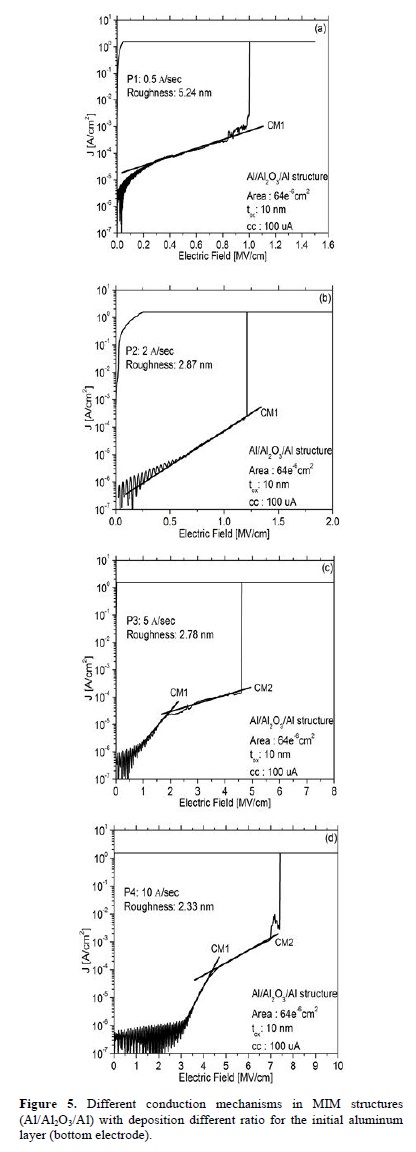
These devices present unipolar switching mode. Here, we only show the first sweep cycle for comparison of the conduction mechanisms in our samples in a clearer, simpler way. In <a href="#f5">figure 5(a)</a>, the structure presents a single conduction mechanism where the best linear fitting was found to be governed by the ohmic model &#91;15&#45;18&#93;. In <a href="#f5">figure (5b)</a>, the MIM structure presents a single conduction mechanism too. Here, the TFL model is the best fit, while the breakdown electric field is slightly greater compared to that of process 1. In <a href="#f5">figure (5c)</a>, we notice that the MIM structure presents two conduction mechanisms: CM1 and CM2, corresponding to ohmic conduction and TFL respectively. Finally, in <a href="#f5">figure (5d)</a> we notice that two different conduction mechanisms appear as well while the best fitting gave the following carrier conduction mechanisms: TFL (CM1) and Poole&#45;Frenkel (CM2).</font></p>  	    <p align="justify"><font face="verdana" size="2">By using different e&#45;beam evaporation conditions that would increase the deposition ratio of the final portion of this aluminum layer (bottom electrode), we promote obtaining aluminum surfaces having different morphological and structural characteristics. This way, different conduction mechanisms during resistive switching are observed. It is highly suggestive to correlate the difference in conduction processes to the surface and therefore, interfacial roughness present in every Metal/Al<sub>2</sub>O<sub>3</sub> interface. Nevertheless, it is also important to consider the chemical changes occurring at these interfaces since lower or higher interfacial roughness would promote different chemical reactions creating interfacial layers (IL) of different characteristics.</font></p>  	    <p align="justify"><font face="verdana" size="2">On the other hand, some memory devices consist of an active electrode (AE) which acts as a source of mobile cations and an electrochemically inert counter&#45;electrode (CE, usually Pt or W) where the cations get reduced to build up the metallic filament &#91;2,15,19&#45;20&#93;. The mechanism for memristance effect in this type of memory device is widely accepted as a redox reaction which involves the oxidation of the AE atoms to produce mobile cations that migrate inside the thin oxide film and are reduced at the CE to form a metallic filament inside the thin oxide film (ON state), and finally, the dissolution and/or rupture of this metallic filament (OFF state) &#91;2, 20&#45;22&#93;. <a href="#f6">Fig. 6</a> shows the I&#45;V characteristics for the remaining Al/Al<sub>2</sub>O<sub>3</sub>/W structures. Al<sub>2</sub>O<sub>3</sub> has thickness of 10nm for <a href="#f6">Fig. 6(a)</a> and 20 nm for <a href="#f6">Fig. 6(b)</a>.</font></p>  	    <p align="justify"><font face="verdana" size="2">In <a href="#f6">figure 6(b)</a>, we notice large electrical instabilities and variations in V<sub>SET</sub>, V<sub>RESET</sub> for many of the measured samples. These variations in V<sub>SET</sub>, V<sub>RESET</sub> are mainly due to large roughness variations of the Metal/Al<sub>2</sub>O<sub>3</sub> interfaces and which could be related to formation of stacking faults during evaporation of these metals at ultra&#45;high vacuum conditions &#91;7,12,15&#93;. By doubling the Al<sub>2</sub>O<sub>3</sub> thickness, the variations in V<sub>SET</sub>, V<sub>RESET</sub> are reduced notably because a thicker oxide would screen&#45;out the surface roughness of both the bottom and top electrodes. In this case the voltage needed to create cyclic resistive switching between HRS and LRS is greater than 13 V, which means that its implementation into a CMOS BEOL process is quite limited. Therefore, it is necessary to minimize the surface roughness of the inert electrode so that smaller oxide thickness can be used and therefore, lower operating voltages.</font></p>  	    ]]></body>
<body><![CDATA[<p align="center"><font face="verdana" size="2"><a name="f6"></a></font></p>  	    <p align="center"><font face="verdana" size="2"><img src="/img/revistas/sv/v27n1/a1f6.jpg"></font></p>  	    <p align="justify"><font face="verdana" size="2">A linear fitting of the I&#45;V curve for the Al/Al<sub>2</sub>O<sub>3</sub>/W structure (Al<sub>2</sub>O<sub>3</sub>= 20 nm, before breakdown) is shown in <a href="#f7">Figure 7</a>. Here the dominant conduction mechanism is Poole&#45;Frenkel. In a similar way to the Al/Al<sub>2</sub>O<sub>3</sub>/Al structure, traps inside the oxide have a major role in the transport of carriers. After filling&#45;up these traps, they would allow generation of additional conductive filaments.</font></p>  	    <p align="center"><font face="verdana" size="2"><a name="f7"></a></font></p>  	    <p align="center"><font face="verdana" size="2"><img src="/img/revistas/sv/v27n1/a1f7.jpg"></font></p>  	    <p align="justify"><font face="verdana" size="2">It is important to mention that both devices (Al/Al2O3/Al and Al/Al2O3/W) show that there is no switching between HRS and LRS until both SET and RESET voltages are reached. This ensures that the stored information will not be lost even if parasite voltages (lower that V<sub>SET</sub> and V<sub>RESET</sub>) are developed or applied on the integrated circuit. <a href="#f8">Fig. 8</a> shows the dependence of gate capacitance density Cg on frequency after C&#45;V measurements at room temperature for MIM structures having 10nm and 20nm in Al<sub>2</sub>O<sub>3</sub> thickness respectively. It is clearly shown that for higher frequencies (up to 3 MHz), lower capacitance density Cg are obtained. Also, the dielectric constant relative to Al<sub>2</sub>O<sub>3</sub> extracted from the C&#45;V curves is &#949;<sub>r</sub> &#126; 7, which suggest that chemical reduction of the Al<sub>2</sub>O<sub>3</sub> to Al<sub>x</sub>O<sub>y</sub> when the gate oxide makes physical contact with the top aluminum electrode occurs. The maximum capacitance at each frequency in the full range is different between one structure and another, as expected. The former is due to the difference in thickness of the aluminum oxide (Cg higher for Al<sub>2</sub>O<sub>3</sub>=10nm). This difference in thickness also influences the behavior of the capacitance Cg at low frequencies but most importantly, it also produce whether a higher degree of electrical instabilities or more uniform I&#45;V characteristics as previously noticed. Therefore, not only the physical thickness of the gate oxide but also, the interfacial roughness of the Metal/Al<sub>2</sub>O<sub>3</sub> interfaces must be taken into account in order to obtain reproducible and long lasting resistive switching properties for these memory devices.</font></p>  	    <p align="center"><font face="verdana" size="2"><a name="f8"></a></font></p>  	    <p align="center"><font face="verdana" size="2"><img src="/img/revistas/sv/v27n1/a1f8.jpg"></font></p>  	    <p>&nbsp;</p>  	    <p align="justify"><font face="verdana" size="2"><b>Conclusions</b></font></p>  	    ]]></body>
<body><![CDATA[<p align="justify"><font face="verdana" size="2">Emergent memory devices which can be vertically integrated into a CMOS&#45;based BEOL processing were fabricated using low thermal conditions and their electrical characteristics were obtained. Vertical integration of memory blocks would increase the integration density of advanced integrated circuits by one order of magnitude while getting close to a true 3&#45;D type integrated circuit manufacturing. From these MIM devices, the memristor effect was observed and more than 4&#45;6 orders of magnitude for the I<sub>OFF</sub>/I<sub>ON</sub> ratios have been obtained after cyclic I&#45;V measurements for all structures. These broad conductivity/resistivity windows are important for long term trapping of carriers within the oxide and therefore, creation/dissolution of conductive filaments which then, will produce the switching between the HRS and LRS. Sharp differences in the conduction mechanisms (before breakdown) were also observed when using whether a highly reactive or an inert metal material as the bottom electrode. Along with the conduction mechanisms, the current compliance as well as the surface roughness of the bottom electrode plays an important role for reliable operation of these memory devices by obtaining reproducible V<sub>SET</sub> and V<sub>RESET</sub> conditions for cyclic voltage sweeps. Finally, an average dielectric constant of &#949;<sub>r</sub> &#126; 7 was extracted from C&#45;V measurements and which suggest a chemical reduction of Al<sub>2</sub>O<sub>3</sub> to Al<sub>x</sub>O<sub>y</sub> when the gate oxide makes physical contact with the top and/or bottom aluminum electrode.</font></p>  	    <p>&nbsp;</p>  	    <p align="justify"><font face="verdana" size="2"><b>References</b></font></p>  	    <!-- ref --><p align="justify"><font face="verdana" size="2">&#91;1&#93; D. B. Strukov, G. S. Snider, D. R. Stewart, and R. S. Williams, Nature, <b>453,</b> 80 (2008).    &nbsp;&nbsp;&nbsp;&nbsp;&nbsp;&nbsp;&nbsp;&nbsp;[&#160;<a href="javascript:void(0);" onclick="javascript: window.open('/scielo.php?script=sci_nlinks&ref=9702886&pid=S1665-3521201400010000100001&lng=','','width=640,height=500,resizable=yes,scrollbars=1,menubar=yes,');">Links</a>&#160;]<!-- end-ref --></font></p>  	    <!-- ref --><p align="justify"><font face="verdana" size="2">&#91;2&#93; R. Waser, R. Dittmann, G. Staikov, and K. Szot, Adv. Mater. <b>21,</b> 2632 (2009).    &nbsp;&nbsp;&nbsp;&nbsp;&nbsp;&nbsp;&nbsp;&nbsp;[&#160;<a href="javascript:void(0);" onclick="javascript: window.open('/scielo.php?script=sci_nlinks&ref=9702888&pid=S1665-3521201400010000100002&lng=','','width=640,height=500,resizable=yes,scrollbars=1,menubar=yes,');">Links</a>&#160;]<!-- end-ref --></font></p>  	    <!-- ref --><p align="justify"><font face="verdana" size="2">&#91;3&#93; S. Yu, B. Lee, and H.&#45;S. P. Wong, edited by J. Wu et al. (Springer, Berlin, 2011).    &nbsp;&nbsp;&nbsp;&nbsp;&nbsp;&nbsp;&nbsp;&nbsp;[&#160;<a href="javascript:void(0);" onclick="javascript: window.open('/scielo.php?script=sci_nlinks&ref=9702890&pid=S1665-3521201400010000100003&lng=','','width=640,height=500,resizable=yes,scrollbars=1,menubar=yes,');">Links</a>&#160;]<!-- end-ref --></font></p>  	    <!-- ref --><p align="justify"><font face="verdana" size="2">&#91;4&#93; H. Y. Lee, P. S. Chen, T. Y. Wu, Y. S. Chen, C. C. Wang, P. J. Tzeng, C. H. Lin, F. Chen, C. H. Lien, and M.&#45;J. Tsai, International Electron Devices Meeting Technical Digest, p. 297 (San Francisco, USA, 2008).    &nbsp;&nbsp;&nbsp;&nbsp;&nbsp;&nbsp;&nbsp;&nbsp;[&#160;<a href="javascript:void(0);" onclick="javascript: window.open('/scielo.php?script=sci_nlinks&ref=9702892&pid=S1665-3521201400010000100004&lng=','','width=640,height=500,resizable=yes,scrollbars=1,menubar=yes,');">Links</a>&#160;]<!-- end-ref --></font></p>  	    <!-- ref --><p align="justify"><font face="verdana" size="2">&#91;5&#93; Y. Wu, S. Yu, B. Lee, and P. Wong, Journal of Applied Physics <b>110,</b> 094104 (2011).    &nbsp;&nbsp;&nbsp;&nbsp;&nbsp;&nbsp;&nbsp;&nbsp;[&#160;<a href="javascript:void(0);" onclick="javascript: window.open('/scielo.php?script=sci_nlinks&ref=9702894&pid=S1665-3521201400010000100005&lng=','','width=640,height=500,resizable=yes,scrollbars=1,menubar=yes,');">Links</a>&#160;]<!-- end-ref --></font></p>  	    <!-- ref --><p align="justify"><font face="verdana" size="2">&#91;6&#93; A. Sawa, Mater. Today, <b>11,</b> 28 (2008).    &nbsp;&nbsp;&nbsp;&nbsp;&nbsp;&nbsp;&nbsp;&nbsp;[&#160;<a href="javascript:void(0);" onclick="javascript: window.open('/scielo.php?script=sci_nlinks&ref=9702896&pid=S1665-3521201400010000100006&lng=','','width=640,height=500,resizable=yes,scrollbars=1,menubar=yes,');">Links</a>&#160;]<!-- end-ref --></font></p>  	    <!-- ref --><p align="justify"><font face="verdana" size="2">&#91;7&#93; J. Su&ntilde;&eacute;, E. Miranda, and D. Jim&eacute;nez, IEEE <b>978,</b> 4577 (2011).    &nbsp;&nbsp;&nbsp;&nbsp;&nbsp;&nbsp;&nbsp;&nbsp;[&#160;<a href="javascript:void(0);" onclick="javascript: window.open('/scielo.php?script=sci_nlinks&ref=9702898&pid=S1665-3521201400010000100007&lng=','','width=640,height=500,resizable=yes,scrollbars=1,menubar=yes,');">Links</a>&#160;]<!-- end-ref --></font></p>  	    <!-- ref --><p align="justify"><font face="verdana" size="2">&#91;8&#93; D. Kim, S. Seo, S. Ahn, D. Suh, M. Lee, B. Park, I. Yoo, I. Baek, H. Kim, E. Yim, J. Lee, S. Park, H. Kim, U. Chung, J. Moon, and B. Ryu, Appl. Phys. Lett., <b>88,</b> 202 (2006).    &nbsp;&nbsp;&nbsp;&nbsp;&nbsp;&nbsp;&nbsp;&nbsp;[&#160;<a href="javascript:void(0);" onclick="javascript: window.open('/scielo.php?script=sci_nlinks&ref=9702900&pid=S1665-3521201400010000100008&lng=','','width=640,height=500,resizable=yes,scrollbars=1,menubar=yes,');">Links</a>&#160;]<!-- end-ref --></font></p>  	    <!-- ref --><p align="justify"><font face="verdana" size="2">&#91;9&#93; J. J. Yang, I. H. Inoue, T. Mikolajick, and C. S. Hwang, MRS Bulletin <b>37,</b> 131 (2012).    &nbsp;&nbsp;&nbsp;&nbsp;&nbsp;&nbsp;&nbsp;&nbsp;[&#160;<a href="javascript:void(0);" onclick="javascript: window.open('/scielo.php?script=sci_nlinks&ref=9702902&pid=S1665-3521201400010000100009&lng=','','width=640,height=500,resizable=yes,scrollbars=1,menubar=yes,');">Links</a>&#160;]<!-- end-ref --></font></p>  	    <!-- ref --><p align="justify"><font face="verdana" size="2">&#91;10&#93; K.M. Kim, D. S. Jeong, C.S. Hwang, Nanotechnology <b>22,</b> 254002 (2011).    &nbsp;&nbsp;&nbsp;&nbsp;&nbsp;&nbsp;&nbsp;&nbsp;[&#160;<a href="javascript:void(0);" onclick="javascript: window.open('/scielo.php?script=sci_nlinks&ref=9702904&pid=S1665-3521201400010000100010&lng=','','width=640,height=500,resizable=yes,scrollbars=1,menubar=yes,');">Links</a>&#160;]<!-- end-ref --></font></p>  	    <!-- ref --><p align="justify"><font face="verdana" size="2">&#91;11&#93; S. H. Chang , J. S. Lee , S. C. Chae , S. B. Lee , C. Liu, B. Kahng , D.&#45;W. Kim, T. W. Noh, Phys. Rev. Lett. <b>102,</b> 026801 (2009).    &nbsp;&nbsp;&nbsp;&nbsp;&nbsp;&nbsp;&nbsp;&nbsp;[&#160;<a href="javascript:void(0);" onclick="javascript: window.open('/scielo.php?script=sci_nlinks&ref=9702906&pid=S1665-3521201400010000100011&lng=','','width=640,height=500,resizable=yes,scrollbars=1,menubar=yes,');">Links</a>&#160;]<!-- end-ref --></font></p>  	    <!-- ref --><p align="justify"><font face="verdana" size="2">&#91;12&#93; I. H. Inoue, S. Yasuda, H. Akinaga, and H. Takagi, <a href="http://arXiv.org/abs/cond-mat/0702564v1" target="_blank">arXiv.org/abs/cond&#45;mat/0702564v1</a>.    &nbsp;&nbsp;&nbsp;&nbsp;&nbsp;&nbsp;&nbsp;&nbsp;[&#160;<a href="javascript:void(0);" onclick="javascript: window.open('/scielo.php?script=sci_nlinks&ref=9702908&pid=S1665-3521201400010000100012&lng=','','width=640,height=500,resizable=yes,scrollbars=1,menubar=yes,');">Links</a>&#160;]<!-- end-ref --></font></p>  	    <!-- ref --><p align="justify"><font face="verdana" size="2">&#91;13&#93; U. Russo, D. Ielmini, C. Cagli, and A. L. Lacaita, IEEE Trans. Electron Devices, <b>56,</b> 193 (2009).    &nbsp;&nbsp;&nbsp;&nbsp;&nbsp;&nbsp;&nbsp;&nbsp;[&#160;<a href="javascript:void(0);" onclick="javascript: window.open('/scielo.php?script=sci_nlinks&ref=9702910&pid=S1665-3521201400010000100013&lng=','','width=640,height=500,resizable=yes,scrollbars=1,menubar=yes,');">Links</a>&#160;]<!-- end-ref --></font></p>  	    <!-- ref --><p align="justify"><font face="verdana" size="2">&#91;14&#93; R. Degraeve, I. S. Jacobs, and C. P. Bean, Techn. Dig. of the IEEE Int. Electron Devices Meeting, pp. 632&#45;635 (2010).    &nbsp;&nbsp;&nbsp;&nbsp;&nbsp;&nbsp;&nbsp;&nbsp;[&#160;<a href="javascript:void(0);" onclick="javascript: window.open('/scielo.php?script=sci_nlinks&ref=9702912&pid=S1665-3521201400010000100014&lng=','','width=640,height=500,resizable=yes,scrollbars=1,menubar=yes,');">Links</a>&#160;]<!-- end-ref --></font></p>  	    <!-- ref --><p align="justify"><font face="verdana" size="2">&#91;15&#93; A. Sleiman, P. W. Sayers, and M. F. Mabrook, Journal of Applied Physics <b>113,</b> 164506 (2013).    &nbsp;&nbsp;&nbsp;&nbsp;&nbsp;&nbsp;&nbsp;&nbsp;[&#160;<a href="javascript:void(0);" onclick="javascript: window.open('/scielo.php?script=sci_nlinks&ref=9702914&pid=S1665-3521201400010000100015&lng=','','width=640,height=500,resizable=yes,scrollbars=1,menubar=yes,');">Links</a>&#160;]<!-- end-ref --></font></p>  	    <!-- ref --><p align="justify"><font face="verdana" size="2">&#91;16&#93; W.S. Lau, Nanyang Technological University (Retired), School of EEE, 639798, Singapore.    &nbsp;&nbsp;&nbsp;&nbsp;&nbsp;&nbsp;&nbsp;&nbsp;[&#160;<a href="javascript:void(0);" onclick="javascript: window.open('/scielo.php?script=sci_nlinks&ref=9702916&pid=S1665-3521201400010000100016&lng=','','width=640,height=500,resizable=yes,scrollbars=1,menubar=yes,');">Links</a>&#160;]<!-- end-ref --></font></p>  	    <!-- ref --><p align="justify"><font face="verdana" size="2">&#91;17&#93; S.M. Sze, Kwok K. Ng, Wiley&#45;Interscience (2007).    &nbsp;&nbsp;&nbsp;&nbsp;&nbsp;&nbsp;&nbsp;&nbsp;[&#160;<a href="javascript:void(0);" onclick="javascript: window.open('/scielo.php?script=sci_nlinks&ref=9702918&pid=S1665-3521201400010000100017&lng=','','width=640,height=500,resizable=yes,scrollbars=1,menubar=yes,');">Links</a>&#160;]<!-- end-ref --></font></p>  	    <!-- ref --><p align="justify"><font face="verdana" size="2">&#91;18&#93; K.Y. Cheong, J.H. Moon, H.J. Kim, W. Bahng, and N&#45;K. Kim, Journal of Applied Physics <b>103,</b> 084113 (2008).    &nbsp;&nbsp;&nbsp;&nbsp;&nbsp;&nbsp;&nbsp;&nbsp;[&#160;<a href="javascript:void(0);" onclick="javascript: window.open('/scielo.php?script=sci_nlinks&ref=9702920&pid=S1665-3521201400010000100018&lng=','','width=640,height=500,resizable=yes,scrollbars=1,menubar=yes,');">Links</a>&#160;]<!-- end-ref --></font></p>  	    <!-- ref --><p align="justify"><font face="verdana" size="2">&#91;19&#93; S. Tappertzhofen, S. Menzel, I. Valov, and R. Waser, Appl. Phys. Lett. <b>99,</b> 203103 (2011).    &nbsp;&nbsp;&nbsp;&nbsp;&nbsp;&nbsp;&nbsp;&nbsp;[&#160;<a href="javascript:void(0);" onclick="javascript: window.open('/scielo.php?script=sci_nlinks&ref=9702922&pid=S1665-3521201400010000100019&lng=','','width=640,height=500,resizable=yes,scrollbars=1,menubar=yes,');">Links</a>&#160;]<!-- end-ref --></font></p>  	    <!-- ref --><p align="justify"><font face="verdana" size="2">&#91;20&#93; R. Bruchhaus, M. Honal, R. Symanczyk, and M. Kund,J. Electrochem. Soc. <b>156,</b> H729 (2009).    &nbsp;&nbsp;&nbsp;&nbsp;&nbsp;&nbsp;&nbsp;&nbsp;[&#160;<a href="javascript:void(0);" onclick="javascript: window.open('/scielo.php?script=sci_nlinks&ref=9702924&pid=S1665-3521201400010000100020&lng=','','width=640,height=500,resizable=yes,scrollbars=1,menubar=yes,');">Links</a>&#160;]<!-- end-ref --></font></p> 	 	    <!-- ref --><p align="justify"><font face="verdana" size="2">&#91;21&#93; K. M. Kim, B. J. Choi, Y. C. Shin, S. Choi, and C. S. Hwang, Appl. Phys. Lett. <b>91,</b> 012907 (2007).    &nbsp;&nbsp;&nbsp;&nbsp;&nbsp;&nbsp;&nbsp;&nbsp;[&#160;<a href="javascript:void(0);" onclick="javascript: window.open('/scielo.php?script=sci_nlinks&ref=9702926&pid=S1665-3521201400010000100021&lng=','','width=640,height=500,resizable=yes,scrollbars=1,menubar=yes,');">Links</a>&#160;]<!-- end-ref --></font></p>  	    <!-- ref --><p align="justify"><font face="verdana" size="2">&#91;22&#93; D.&#45;H. Kwon, K. M. Kim, J. H. Jang, J. M. Jeon, M. H. Lee, G. H. Kim, X.&#45;S. Li, G.S. Park, B. Lee, S. Han, M. Kim, and C.S. Hwang, Nat. Nanotechnol. <b>5,</b> 148 (2010).    &nbsp;&nbsp;&nbsp;&nbsp;&nbsp;&nbsp;&nbsp;&nbsp;[&#160;<a href="javascript:void(0);" onclick="javascript: window.open('/scielo.php?script=sci_nlinks&ref=9702928&pid=S1665-3521201400010000100022&lng=','','width=640,height=500,resizable=yes,scrollbars=1,menubar=yes,');">Links</a>&#160;]<!-- end-ref --></font></p>      ]]></body><back>
<ref-list>
<ref id="B1">
<label>1</label><nlm-citation citation-type="journal">
<person-group person-group-type="author">
<name>
<surname><![CDATA[Strukov]]></surname>
<given-names><![CDATA[D. B.]]></given-names>
</name>
<name>
<surname><![CDATA[Snider]]></surname>
<given-names><![CDATA[G. S.]]></given-names>
</name>
<name>
<surname><![CDATA[Stewart]]></surname>
<given-names><![CDATA[D. R.]]></given-names>
</name>
<name>
<surname><![CDATA[Williams]]></surname>
<given-names><![CDATA[R. S.]]></given-names>
</name>
</person-group>
<source><![CDATA[Nature]]></source>
<year>2008</year>
<volume>453</volume>
<page-range>80</page-range></nlm-citation>
</ref>
<ref id="B2">
<label>2</label><nlm-citation citation-type="journal">
<person-group person-group-type="author">
<name>
<surname><![CDATA[Waser]]></surname>
<given-names><![CDATA[R.]]></given-names>
</name>
<name>
<surname><![CDATA[Dittmann]]></surname>
<given-names><![CDATA[R.]]></given-names>
</name>
<name>
<surname><![CDATA[Staikov]]></surname>
<given-names><![CDATA[G.]]></given-names>
</name>
<name>
<surname><![CDATA[Szot]]></surname>
<given-names><![CDATA[K.]]></given-names>
</name>
</person-group>
<source><![CDATA[Adv. Mater.]]></source>
<year>2009</year>
<volume>21</volume>
<page-range>2632</page-range></nlm-citation>
</ref>
<ref id="B3">
<label>3</label><nlm-citation citation-type="book">
<person-group person-group-type="author">
<name>
<surname><![CDATA[Yu]]></surname>
<given-names><![CDATA[S.]]></given-names>
</name>
<name>
<surname><![CDATA[Lee]]></surname>
<given-names><![CDATA[B.]]></given-names>
</name>
<name>
<surname><![CDATA[Wong]]></surname>
<given-names><![CDATA[H.-S. P.]]></given-names>
</name>
<name>
<surname><![CDATA[Wu]]></surname>
<given-names><![CDATA[J.]]></given-names>
</name>
</person-group>
<source><![CDATA[]]></source>
<year>2011</year>
<publisher-loc><![CDATA[Berlin ]]></publisher-loc>
<publisher-name><![CDATA[Springer]]></publisher-name>
</nlm-citation>
</ref>
<ref id="B4">
<label>4</label><nlm-citation citation-type="book">
<person-group person-group-type="author">
<name>
<surname><![CDATA[Lee]]></surname>
<given-names><![CDATA[H. Y.]]></given-names>
</name>
<name>
<surname><![CDATA[Chen]]></surname>
<given-names><![CDATA[P. S.]]></given-names>
</name>
<name>
<surname><![CDATA[Wu]]></surname>
<given-names><![CDATA[T. Y.]]></given-names>
</name>
<name>
<surname><![CDATA[Chen]]></surname>
<given-names><![CDATA[Y. S.]]></given-names>
</name>
<name>
<surname><![CDATA[Wang]]></surname>
<given-names><![CDATA[C. C.]]></given-names>
</name>
<name>
<surname><![CDATA[Tzeng]]></surname>
<given-names><![CDATA[P. J.]]></given-names>
</name>
<name>
<surname><![CDATA[Lin]]></surname>
<given-names><![CDATA[C. H.]]></given-names>
</name>
<name>
<surname><![CDATA[Chen]]></surname>
<given-names><![CDATA[F.]]></given-names>
</name>
<name>
<surname><![CDATA[Lien]]></surname>
<given-names><![CDATA[C. H.]]></given-names>
</name>
<name>
<surname><![CDATA[Tsai]]></surname>
<given-names><![CDATA[M.-J.]]></given-names>
</name>
</person-group>
<source><![CDATA[International Electron Devices Meeting Technical Digest]]></source>
<year>2008</year>
<page-range>297</page-range><publisher-loc><![CDATA[San Francisco ]]></publisher-loc>
<publisher-name><![CDATA[USA]]></publisher-name>
</nlm-citation>
</ref>
<ref id="B5">
<label>5</label><nlm-citation citation-type="journal">
<person-group person-group-type="author">
<name>
<surname><![CDATA[Wu]]></surname>
<given-names><![CDATA[Y.]]></given-names>
</name>
<name>
<surname><![CDATA[Yu]]></surname>
<given-names><![CDATA[S.]]></given-names>
</name>
<name>
<surname><![CDATA[Lee]]></surname>
<given-names><![CDATA[B.]]></given-names>
</name>
<name>
<surname><![CDATA[Wong]]></surname>
<given-names><![CDATA[P.]]></given-names>
</name>
</person-group>
<source><![CDATA[Journal of Applied Physics]]></source>
<year>2011</year>
<volume>110</volume>
<page-range>094104</page-range></nlm-citation>
</ref>
<ref id="B6">
<label>6</label><nlm-citation citation-type="journal">
<person-group person-group-type="author">
<name>
<surname><![CDATA[Sawa]]></surname>
<given-names><![CDATA[A.]]></given-names>
</name>
</person-group>
<source><![CDATA[Mater. Today]]></source>
<year>2008</year>
<volume>11</volume>
<page-range>28</page-range></nlm-citation>
</ref>
<ref id="B7">
<label>7</label><nlm-citation citation-type="journal">
<person-group person-group-type="author">
<name>
<surname><![CDATA[Suñé]]></surname>
<given-names><![CDATA[J.]]></given-names>
</name>
<name>
<surname><![CDATA[Miranda]]></surname>
<given-names><![CDATA[E.]]></given-names>
</name>
<name>
<surname><![CDATA[Jiménez]]></surname>
<given-names><![CDATA[D.]]></given-names>
</name>
</person-group>
<source><![CDATA[IEEE]]></source>
<year>2011</year>
<volume>978</volume>
<page-range>4577</page-range></nlm-citation>
</ref>
<ref id="B8">
<label>8</label><nlm-citation citation-type="journal">
<person-group person-group-type="author">
<name>
<surname><![CDATA[Kim]]></surname>
<given-names><![CDATA[D.]]></given-names>
</name>
<name>
<surname><![CDATA[Seo]]></surname>
<given-names><![CDATA[S.]]></given-names>
</name>
<name>
<surname><![CDATA[Ahn]]></surname>
<given-names><![CDATA[S.]]></given-names>
</name>
<name>
<surname><![CDATA[Suh]]></surname>
<given-names><![CDATA[D.]]></given-names>
</name>
<name>
<surname><![CDATA[Lee]]></surname>
<given-names><![CDATA[M.]]></given-names>
</name>
<name>
<surname><![CDATA[Park]]></surname>
<given-names><![CDATA[B.]]></given-names>
</name>
<name>
<surname><![CDATA[Yoo]]></surname>
<given-names><![CDATA[I.]]></given-names>
</name>
<name>
<surname><![CDATA[Baek]]></surname>
<given-names><![CDATA[I.]]></given-names>
</name>
<name>
<surname><![CDATA[Kim]]></surname>
<given-names><![CDATA[H.]]></given-names>
</name>
<name>
<surname><![CDATA[Yim]]></surname>
<given-names><![CDATA[E.]]></given-names>
</name>
<name>
<surname><![CDATA[Lee]]></surname>
<given-names><![CDATA[J.]]></given-names>
</name>
<name>
<surname><![CDATA[Park]]></surname>
<given-names><![CDATA[S.]]></given-names>
</name>
<name>
<surname><![CDATA[Kim]]></surname>
<given-names><![CDATA[H.]]></given-names>
</name>
<name>
<surname><![CDATA[Chung]]></surname>
<given-names><![CDATA[U.]]></given-names>
</name>
<name>
<surname><![CDATA[Moon]]></surname>
<given-names><![CDATA[J.]]></given-names>
</name>
<name>
<surname><![CDATA[Ryu]]></surname>
<given-names><![CDATA[B.]]></given-names>
</name>
</person-group>
<source><![CDATA[Appl. Phys. Lett.]]></source>
<year>2006</year>
<volume>88</volume>
<page-range>202</page-range></nlm-citation>
</ref>
<ref id="B9">
<label>9</label><nlm-citation citation-type="journal">
<person-group person-group-type="author">
<name>
<surname><![CDATA[Yang]]></surname>
<given-names><![CDATA[J. J.]]></given-names>
</name>
<name>
<surname><![CDATA[Inoue]]></surname>
<given-names><![CDATA[I. H.]]></given-names>
</name>
<name>
<surname><![CDATA[Mikolajick]]></surname>
<given-names><![CDATA[T.]]></given-names>
</name>
<name>
<surname><![CDATA[Hwang]]></surname>
<given-names><![CDATA[C. S.]]></given-names>
</name>
</person-group>
<source><![CDATA[MRS Bulletin]]></source>
<year>2012</year>
<volume>37</volume>
<page-range>131</page-range></nlm-citation>
</ref>
<ref id="B10">
<label>10</label><nlm-citation citation-type="journal">
<person-group person-group-type="author">
<name>
<surname><![CDATA[Kim]]></surname>
<given-names><![CDATA[K.M.]]></given-names>
</name>
<name>
<surname><![CDATA[Jeong]]></surname>
<given-names><![CDATA[D. S.]]></given-names>
</name>
<name>
<surname><![CDATA[Hwang]]></surname>
<given-names><![CDATA[C.S.]]></given-names>
</name>
</person-group>
<source><![CDATA[Nanotechnology]]></source>
<year>2011</year>
<volume>22</volume>
<page-range>254002</page-range></nlm-citation>
</ref>
<ref id="B11">
<label>11</label><nlm-citation citation-type="journal">
<person-group person-group-type="author">
<name>
<surname><![CDATA[Chang]]></surname>
<given-names><![CDATA[S. H.]]></given-names>
</name>
<name>
<surname><![CDATA[Lee]]></surname>
<given-names><![CDATA[J. S.]]></given-names>
</name>
<name>
<surname><![CDATA[Chae]]></surname>
<given-names><![CDATA[S. C.]]></given-names>
</name>
<name>
<surname><![CDATA[Lee]]></surname>
<given-names><![CDATA[S. B.]]></given-names>
</name>
<name>
<surname><![CDATA[Liu]]></surname>
<given-names><![CDATA[C.]]></given-names>
</name>
<name>
<surname><![CDATA[Kahng]]></surname>
<given-names><![CDATA[B.]]></given-names>
</name>
<name>
<surname><![CDATA[Kim]]></surname>
<given-names><![CDATA[D.-W.]]></given-names>
</name>
<name>
<surname><![CDATA[Noh]]></surname>
<given-names><![CDATA[T. W.]]></given-names>
</name>
</person-group>
<source><![CDATA[Phys. Rev. Lett.]]></source>
<year>2009</year>
<volume>102</volume>
<page-range>026801</page-range></nlm-citation>
</ref>
<ref id="B12">
<label>12</label><nlm-citation citation-type="">
<person-group person-group-type="author">
<name>
<surname><![CDATA[Inoue]]></surname>
<given-names><![CDATA[I. H.]]></given-names>
</name>
<name>
<surname><![CDATA[Yasuda]]></surname>
<given-names><![CDATA[S.]]></given-names>
</name>
<name>
<surname><![CDATA[Akinaga]]></surname>
<given-names><![CDATA[H.]]></given-names>
</name>
<name>
<surname><![CDATA[Takagi]]></surname>
<given-names><![CDATA[H.]]></given-names>
</name>
</person-group>
<source><![CDATA[]]></source>
<year></year>
</nlm-citation>
</ref>
<ref id="B13">
<label>13</label><nlm-citation citation-type="journal">
<person-group person-group-type="author">
<name>
<surname><![CDATA[Russo]]></surname>
<given-names><![CDATA[U.]]></given-names>
</name>
<name>
<surname><![CDATA[Ielmini]]></surname>
<given-names><![CDATA[D.]]></given-names>
</name>
<name>
<surname><![CDATA[Cagli]]></surname>
<given-names><![CDATA[C.]]></given-names>
</name>
<name>
<surname><![CDATA[Lacaita]]></surname>
<given-names><![CDATA[A. L.]]></given-names>
</name>
</person-group>
<source><![CDATA[IEEE Trans. Electron Devices]]></source>
<year>2009</year>
<volume>56</volume>
<page-range>193</page-range></nlm-citation>
</ref>
<ref id="B14">
<label>14</label><nlm-citation citation-type="">
<person-group person-group-type="author">
<name>
<surname><![CDATA[Degraeve]]></surname>
<given-names><![CDATA[R.]]></given-names>
</name>
<name>
<surname><![CDATA[Jacobs]]></surname>
<given-names><![CDATA[I. S.]]></given-names>
</name>
<name>
<surname><![CDATA[Bean]]></surname>
<given-names><![CDATA[C. P.]]></given-names>
</name>
</person-group>
<source><![CDATA[Techn. Dig. of the IEEE Int. Electron Devices Meeting]]></source>
<year>2010</year>
<page-range>632-635</page-range></nlm-citation>
</ref>
<ref id="B15">
<label>15</label><nlm-citation citation-type="journal">
<person-group person-group-type="author">
<name>
<surname><![CDATA[Sleiman]]></surname>
<given-names><![CDATA[A.]]></given-names>
</name>
<name>
<surname><![CDATA[Sayers]]></surname>
<given-names><![CDATA[P. W.]]></given-names>
</name>
<name>
<surname><![CDATA[Mabrook]]></surname>
<given-names><![CDATA[M. F.]]></given-names>
</name>
</person-group>
<source><![CDATA[Journal of Applied Physics]]></source>
<year>2013</year>
<volume>113</volume>
<page-range>164506</page-range></nlm-citation>
</ref>
<ref id="B16">
<label>16</label><nlm-citation citation-type="book">
<person-group person-group-type="author">
<name>
<surname><![CDATA[Lau]]></surname>
<given-names><![CDATA[W.S.]]></given-names>
</name>
</person-group>
<source><![CDATA[]]></source>
<year></year>
<page-range>639798</page-range><publisher-name><![CDATA[Nanyang Technological University (Retired), School of EEE]]></publisher-name>
</nlm-citation>
</ref>
<ref id="B17">
<label>17</label><nlm-citation citation-type="book">
<person-group person-group-type="author">
<name>
<surname><![CDATA[Sze]]></surname>
<given-names><![CDATA[S.M.]]></given-names>
</name>
<name>
<surname><![CDATA[Ng]]></surname>
<given-names><![CDATA[Kwok K.]]></given-names>
</name>
</person-group>
<source><![CDATA[]]></source>
<year>2007</year>
<publisher-name><![CDATA[Wiley-Interscience]]></publisher-name>
</nlm-citation>
</ref>
<ref id="B18">
<label>18</label><nlm-citation citation-type="journal">
<person-group person-group-type="author">
<name>
<surname><![CDATA[Cheong]]></surname>
<given-names><![CDATA[K.Y.]]></given-names>
</name>
<name>
<surname><![CDATA[Moon]]></surname>
<given-names><![CDATA[J.H.]]></given-names>
</name>
<name>
<surname><![CDATA[Kim]]></surname>
<given-names><![CDATA[H.J.]]></given-names>
</name>
<name>
<surname><![CDATA[Bahng]]></surname>
<given-names><![CDATA[W.]]></given-names>
</name>
<name>
<surname><![CDATA[Kim]]></surname>
<given-names><![CDATA[N-K.]]></given-names>
</name>
</person-group>
<source><![CDATA[Journal of Applied Physics]]></source>
<year>2008</year>
<volume>103</volume>
<page-range>084113</page-range></nlm-citation>
</ref>
<ref id="B19">
<label>19</label><nlm-citation citation-type="journal">
<person-group person-group-type="author">
<name>
<surname><![CDATA[Tappertzhofen]]></surname>
<given-names><![CDATA[S.]]></given-names>
</name>
<name>
<surname><![CDATA[Menzel]]></surname>
<given-names><![CDATA[S.]]></given-names>
</name>
<name>
<surname><![CDATA[Valov]]></surname>
<given-names><![CDATA[I.]]></given-names>
</name>
<name>
<surname><![CDATA[Waser]]></surname>
<given-names><![CDATA[R.]]></given-names>
</name>
</person-group>
<source><![CDATA[Appl. Phys. Lett.]]></source>
<year>2011</year>
<volume>99</volume>
<page-range>203103</page-range></nlm-citation>
</ref>
<ref id="B20">
<label>20</label><nlm-citation citation-type="journal">
<person-group person-group-type="author">
<name>
<surname><![CDATA[Bruchhaus]]></surname>
<given-names><![CDATA[R.]]></given-names>
</name>
<name>
<surname><![CDATA[Honal]]></surname>
<given-names><![CDATA[M.]]></given-names>
</name>
<name>
<surname><![CDATA[Symanczyk]]></surname>
<given-names><![CDATA[R.]]></given-names>
</name>
<name>
<surname><![CDATA[Kund]]></surname>
<given-names><![CDATA[M.]]></given-names>
</name>
</person-group>
<source><![CDATA[J. Electrochem. Soc.]]></source>
<year>2009</year>
<volume>156</volume>
<page-range>H729</page-range></nlm-citation>
</ref>
<ref id="B21">
<label>21</label><nlm-citation citation-type="journal">
<person-group person-group-type="author">
<name>
<surname><![CDATA[Kim]]></surname>
<given-names><![CDATA[K. M.]]></given-names>
</name>
<name>
<surname><![CDATA[Choi]]></surname>
<given-names><![CDATA[B. J.]]></given-names>
</name>
<name>
<surname><![CDATA[Shin]]></surname>
<given-names><![CDATA[Y. C.]]></given-names>
</name>
<name>
<surname><![CDATA[Choi]]></surname>
<given-names><![CDATA[S.]]></given-names>
</name>
<name>
<surname><![CDATA[Hwang]]></surname>
<given-names><![CDATA[C. S.]]></given-names>
</name>
</person-group>
<source><![CDATA[Appl. Phys. Lett.]]></source>
<year>2007</year>
<volume>91</volume>
<page-range>012907</page-range></nlm-citation>
</ref>
<ref id="B22">
<label>22</label><nlm-citation citation-type="journal">
<person-group person-group-type="author">
<name>
<surname><![CDATA[Kwon]]></surname>
<given-names><![CDATA[D.-H.]]></given-names>
</name>
<name>
<surname><![CDATA[Kim]]></surname>
<given-names><![CDATA[K. M.]]></given-names>
</name>
<name>
<surname><![CDATA[Jang]]></surname>
<given-names><![CDATA[J. H.]]></given-names>
</name>
<name>
<surname><![CDATA[Jeon]]></surname>
<given-names><![CDATA[J. M.]]></given-names>
</name>
<name>
<surname><![CDATA[Lee]]></surname>
<given-names><![CDATA[M. H.]]></given-names>
</name>
<name>
<surname><![CDATA[Kim]]></surname>
<given-names><![CDATA[G. H.]]></given-names>
</name>
<name>
<surname><![CDATA[Li]]></surname>
<given-names><![CDATA[X.-S.]]></given-names>
</name>
<name>
<surname><![CDATA[Park]]></surname>
<given-names><![CDATA[G.S.]]></given-names>
</name>
<name>
<surname><![CDATA[Lee]]></surname>
<given-names><![CDATA[B.]]></given-names>
</name>
<name>
<surname><![CDATA[Han]]></surname>
<given-names><![CDATA[S.]]></given-names>
</name>
<name>
<surname><![CDATA[Kim]]></surname>
<given-names><![CDATA[M.]]></given-names>
</name>
<name>
<surname><![CDATA[Hwang]]></surname>
<given-names><![CDATA[C.S.]]></given-names>
</name>
</person-group>
<source><![CDATA[Nat. Nanotechnol.]]></source>
<year>2010</year>
<volume>5</volume>
<page-range>148</page-range></nlm-citation>
</ref>
</ref-list>
</back>
</article>
