


Servicios Personalizados
Revista
Articulo
 Inglés (pdf)
 Artículo en XML
 Referencias del artículo
 Enviar artículo por email
Indicadores
-
 Citado por SciELO
 -
 Accesos
Links relacionados
-
 Similares en
SciELO
Similares en
SciELO
Compartir

 Permalink
Nova scientia
versión On-line ISSN 2007-0705
Nova scientia vol.2 no.4 León oct. 2010
Ciencias Naturales e Ingenierías
Electronic Properties of III-V Semiconductors under [111] Uniaxial Strain; a Tight-Binding Approach: II. Antimonides and Phosphides
Propiedades electrónicas de semiconductores III-V sometidos a tensión uniaxial en la dirección [111]; un enfoque según el método tight-binding: II. Antimoniuros y Fosfuros
J. Juan Martín Mozo1,2 y Miguel E. Mora-Ramos3
1 Centro de Investigación en Ingeniería y Ciencias Aplicadas (CIICAP). Universidad Autónoma del Estado de Morelos. Cuernavaca. México.
2 Centro de Investigación en Dispositivos Semiconductores-ICUAP, Benemérita Universidad Autónoma de Puebla. México.
3 Facultad de Ciencias, Universidad Autónoma del Estado de Morelos. México.
Miguel E. Mora-Ramos. E-mail: memora@uaem.mx
Recepción: 23-02-10
Aceptación: 19-04-10
Abstract
The sp3s*d5 empirical tight-binding approach is used to study some properties of the electronic structure in a group of III-V zincblende semiconductors which are of most intersest to electronics and optoelectronics. Particularly, it is investigated the influence of [111] uniaxial strain upon these properties. We make use of a formulation outlined in the first part of this work [Mora-Ramos 2009]. Special attention is paid to the inclusion of the internal deformation effect. We present the variation of the Γ-, X- and L-related energy gaps and conduction band effective masses as functions of the uniaxial strain in the case of AlP, InP, AlSb, GaSb, and InSb. Fitting expressions for the main energy band gaps are reported for these five materials. A strong strain-induced non-linear behavior of these quantities as well as of the conduction band effective masses is observed.
Keywords: tight-binding, III-V materials, electronic structure, uniaxial strain.
Resumen
Empleando un esquema de cálculo tight-binding que usa una base de orbitales sp3s*d5, se estudian propiedades de la estructura electrónica de un grupo de materiales semiconductores III-V los cuales son de interés para la tecnología de dispositivos electrónicos y optoelectrónicos. En específico, se analiza la influencia sobre estas propiedades de una tensión aplicada según la dirección cristalográfica [111], haciendo uso de una formulación presentada en la primera parte del trabajo [Mora-Ramos 2009]. Especial atención se presta a la inclusión del efecto de deformación interna de la red cristalina. Para cada material de los estudiados presentamos las dependencias de las brechas energéticas asociadas a los puntos Γ, X y L de la zona de Brillouin como funciones de la tensión uniaxial en AlP, InP, AlSb, GaSb, InSb. Asimismo, reportamos expresiones de ajuste para los valores de las principales brechas energéticas en esos cinco materiales. Se detecta una fuerte dependencia no lineal de estas magnitudes, así como de las masas efectivas de conducción, con la tensión.
Palabras Clave: tight-binding, materiales III-V, estructura electrónica, tensión uniaxial.
Introduction
In the first part of this work [Mora-Ramos 2009] (hereafter referred as I) we presented a study of the electronic properties of four III-V semiconductors (AlAs, GaAs, GaP and InAs) within the sp3s*d5 empirical tight-binding formalism. The particular feature of such investigation is the presence of [111]-oriented uniaxial strain in the crystal. As an outcome of the calculation, the effects of the strain on the electron energy band structure as well as on the Γ, X and L energy gaps and conduction band effective masses were reported.
This second part deals with the remaining III-V semiconducting crystals with the exception of nitrides, which deserve a separate communication. Again, an empirical tight-binding analysis is used to investigate the influence of [111] uniaxial strain onto the electronic properties of bulk AlP, InP, AlSb, GaSb, and InSb.
Although less widely considered if compared with those studied in I, these five materials have found important applications in the fields of electronics and optoelectronics. AlP is usually alloyed with other binary materials for applications in devices such as light-emitting diodes (e.g. AlGaInP). InP is used in high-power and high-frequency electronics because of its large electron mobility (~5400 cm2 V-1s-1). It also has a direct bandgap, making it useful for optoelectronics devices like laser diodes. InP is also used as a substrate for epitaxial indium gallium arsenide based opto-electronic devices. Indium antimonide is a narrow gap semiconductor material with a very high electron mobility (~7.7·104 cm2V-1s-1) used in infrared detectors, including thermal imaging cameras, FLIR systems, infrared homing missile guidance systems, and in infrared astronomy. Another application of InSb is as terahertz radiation source as it is a strong photo-Dember emitter. On the other hand, GaSb can be used in the fabrication of infrared detectors, infrared LEDs and lasers and transistors, as well as thermo-photovoltaic systems. AlSb is mostly used in alloys with other III-V semiconductors to produce ternary materials like AlInSb, AlGaSb and AlAsSb. There are previous communications on the use of AlSb as a component in superlattices together with InAs. These are proposed for using as cladding layers in semiconductor diode lasers [Chow 1995]. Semi-metallic InAs/GaSb quantum wells exhibiting negative persistent photoconductivity were also reported some years ago [Schets 1999]. A review on the use of antimonide-based compound semiconductors for electronic devices can be found in reference [Bennett 2005].
With respect to deformation-related effects involving these III-V materials it is possible to mention the study of the phenomenon of strain relaxation in AlSb/GaSb heterostructures [Sarney 2002]. In that work it was found that AlSb remains highly strained for film thicknesses above 1000 Ǻ when it is grown on GaSb by molecular beam epitaxy. Even for 2 μm films a significant strain of ~18% was retained. In the case of III-V phosphides we can mention very recent calculations on the effect of high pressure on elastic and structural properties using the full potential augmented plane wave plus local orbital method [Bouhemadou 2009].
There are still some reservations among the scientific community regarding the use of the fictitious s* orbital once it has been already introduced the full set of five d atomic orbitals into the basis. However, as it has been put forward, in the case of diamond and zincblende III-V crystals it is necessary to keep this orbital within the description if one is limited to use only a first-neighbor approximation. Besides the pioneering works of Jancu et al. [Jancu 1998, Scholz 2000], some other authors have confirmed such a need [Boykin 2002, Niquet 2009]. Undoubtedly, using a first-neighbor configuration facilitates both the analytical and numerical treatment of the calculation of the electronic properties, and it is easier to formulate via a comparison with first-principle pseudopotential approaches. Even, there have been recent modifications to the first-neighbor sp3s*d5 formalism to more properly deal with tetragonal and trigonal deformations as that precisely considered in the present work [Jancu 2007]. However, the corresponding modified parameterization has been so far reported only for the case of Ge. For that reason, we shall continue using the original TB parameters of the 1998 article [Jancu 1998]. The aim of this second part is to present the results obtained within our work for the cases of III-V antimonides, and aluminum and indium phosphides. We think that a more complete information regarding the behavior of main electronic properties of these crystals as functions of [111] uniaxial strain would always be of significant help for researchers investigating electron and hole states in [111]-oriented strained heterostructures based in these materials.
Another phenomenon that will become apparent from the results of the present work is that of the so-called band inversion. This effect was first reported in very narrow gap materials as PbxSn1-xTe [Dimmock 1966], and Pb1-xSnxSe [Strauss 1967]. These materials have the rocksalt structure and exhibit the inversion in the band structure upon variation of both temperature and tin molar fraction, and also when hydrostatic pressure is applied [Martínez 1973]. It happens that the upper valence band edge at the L point of the Brilloin zone and the lower conduction band minimum at the same position approach each other when the mentioned parameters are changed. Then, at a certain set of values for them, the bands touch leading to a zero gap state. After that, the ulterior variation of those conditions makes the material to have a "negative" energy band gap. The physical reason for this to occur is associated to the relativistic shifts of Pb and Sn.
On the other hand, the phenomenon of band inversion can be also attributed to a lowering in the translational symmetry of the crystal. That situation was theoretically studied in the case of III-V zincblende heterostructures where the crystal translational symmetry is broken along the structure growth direction. In 1982 Milanović and Tjapkin showed the existence of zero gap states in AlxGa1-xAs-GaAs superlattices [Milanović, 1982] due to the variation of layer width and aluminum molar fraction. Later on, the presence of zero gap states and band inversion was shown to exist in the case of InAs-GaSb superlattices by de Dios and Gondar [de Dios 1985]. These latter structures are of the second-type. That is, the confining layers are different for electrons and holes, and the bottom of the quantum well for the holes in layer B is energetically very close to the bottom of the quantum well for electrons in layer A. Again, due to the variations of layer width and confining potential height, V, a state of zero gap may appear. The conduction band bottom corresponds to an even state and the valence band top to an odd state. For a fixed layer width, if V increases, those bands approach until they touch each other and then move away after crossing: a band inversion phenomenon is present. In this article we also discuss the presence of the band inversion induced by uniaxial strain in the case of the narrower gap III-V zincblende semiconductors.
The mathematical aspects of the model are discussed in detail in sections 1 and 2 of I. Elastic constants are taken from the reports by Li and Vurgaftman et al. [Li 2000, Vurgaftman 2001]. The values for the internal deformation parameters were taken from the work of Muramatsu and Kitamura [Muramatsu 1993].
In the next section we present and discuss the results for the electronic dispersion relations, together with the variations of the main energy gaps and conduction effective masses as functions of the strain. Last section will then be devoted to express our conclusions.
Results and discussion
As a direct outcome of the process of diagonalizing the sp3s*d5 TB matrix Hamiltonian constructed for the strained basis, figures 1 (2, 3, 4) to 5 show the [111] dispersion relations of the upper three valence bands and the lower two conduction bands along the L → Γ and Γ → X directions in the semiconductor Brillouin Zone. They correspond to AlP, InP, AlSb, GaSb, and InSb, respectively. Three different values of the [111] strain, εp, are considered, including the zero strain case. They are taken going from -5 % (compressive in-plane deformation) to 5 % (tensile in-plane deformation).
It is seen that strained crystals show significant differences in their electronic structure compared to the unstrained ones. It must be mentioned that although the energy dispersion relations show -in some cases-- the presence of apparent accidental degeneracies; in fact what we really have is the appearance of band anticrossings. This is seen, for instance, in the case of the upper valence bands near the Brillouin zone center in the L → Γ direction for the five materials under negative in-plane strain. This feature can also be observed for zero strain in AlP, involving the two lower conduction bands in the Γ →X direction. The scale chosen for the figures does not allow to visualize such anticrossings properly. However, the same enhancement procedure made in the case of arsenides and gallium phosphide in I allows us to readily identify them.
The influence of a [111] uniaxial strain on the conduction and valence band edges is better understood if we observe the figure 6. It can be seen that, in general, the energy position of the zone-center upper edge of the light and heavy hole valence bands tends to shift upwards when uniaxial strain goes from larger tensile values to larger compressive values (here, it must be kept in mind that in-plane deformation is opposite in sign to the uniaxial one as indicated in equations (2) and (5) of I). The only exceptions to this behavior are the cases of the light hole band edge in InSb and the heavy hole band edge in GaSb which are decreasing functions starting from certain value of the in-plane strain in the positive region.
Also, as general tendencies, they can be mentioned the increasing and decreasing variations of X-and L-related conduction band edges respectively. However, in the case of the Γ first conduction band state it is possible to observe some interesting aspects which are summarized as follows.
In the negative in-plane deformation region, the Γ conduction band edge is a decreasing function of the deformation all the way as εp goes towards zero, with the exception of the two aluminum compounds. In the cases of AlP and AlSb one can detect a significant non-linear variation which begins with an increment as long as the magnitude of the deformation diminishes. Then, it reaches a maximum and starts decreasing continuously throughout the smaller negative and the positive values.
The InP shows the conduction Γ band edge to be a monotonically decreasing function for the entire range of variation of the in-plane deformation εp. However, in the positive region of values for this quantity, one can detect a sudden change of monotony of this particular energy state in the cases of GaSb and InSb. The point at which this inflexion is detected corresponds to uniaxial [111] compressive strains (ε⊥) of approximately 1.79% (GaSb) and 0.7% (InSb).
Physically speaking, what we actually have under such conditions is a phenomenon of strain-induced band inversion, and we will refer to it more extensively in a discussion below.
For a separate analysis of the variation of the [111] main energy gaps in the four materials figures 7, 8, 9, 10, and 11 show, in AlP, InP, AlSb, GaSb, and InSb, respectively, the behaviors of these quantities for the Γ (EgΓ - blue lines), X (EgX -red lines), and L (EgL -purple lines) points of the Brillouin zone, measured with respect to the top of the corresponding valence band at the zone center.
In the case of AlP (figure 7), it is seen that this X-related indirect gap material different behaviors for each of the three main calculated energy gaps. The X-gap is a slight decreasing function of the in-plane deformation along the negative and positive intervals of values of εp considered. L-related energy gap is a more steeped decreasing function along the entire range of in-plane deformation, whilst the Γ-gap shows a mixed behavior. In the negative εp region, EgΓ has a strong non-linear variation. It is first an increasing function and reaches a maximum value around εp ~ 2%. Then it decreases all the way throughout the rest of the deformation interval. It can be inferred that, for high enough strain values, these three gap functions will intersect, and some kind of indirect-to-indirect or indirect-to-direct gap transitions will occur. But this would happen for values of strain that are not considered in this work. It remains to be seen if such high strain values still retain some experimental sense.
According to our results, InP is a direct gap semiconductor until [111]-related in-plane deformation reaches a compressive magnitude of approximately 4.3% (figure 8). In this situation, there occurs a strain-induced direct-to-indirect gap transition and the material becomes a X-related indirect gap semiconductor. Again, in this material, EgX is a slight decreasing function of the deformation. Both EgΓ and EgL are more steeped decreasing functions of the uniaxial strain from large tensile to large compressive values.
In the case of AlSb, this indirect gap material seems to undergo a strain-induced transition from indirect to direct energy bandgap character for compressive uniaxial strains leading to tensile in-plane deformation around 2% (figure 9). The monotony behavior of EgX keeps the features discussed above for the AlP and InP. Likewise, EgL continues to exhibit a decreasing variation for the whole range of deformation considered. A quite significant non-linearity is observed for EgΓ in the negative interval of εp On the other hand, in the positive region of the deformation, this gap is a decreasing function of the deformation.
Considering the negative in-plane deformation region of GaSb (figure 10), one can observe that strain induces a Γ-direct-to-indirect-X-gap transition for a rather low value of the tensile [111] uniaxial deformation (ε⊥ ~ 0.53%, which corresponds to εp ~ -1% ). This is a fact to take into account in the analysis of the electronic states in [111]-oriented GaSb-based superlattices. The positive in-plane deformation region in figure 10 shows decreasing variation of the three main energy gaps until the point for band inversion is reached (εp -3.7%). For higher values of strain we have depicted the so-called negative gap associated with the energy difference between the above-located "heavy-hole valence band" and the "first electron conduction band" at a lower position. This energy difference is -in magnitude- an increasing function of the strain, although a rather strong nonlinearity is detected for its variation. It is worth mentioning at this point that the functions EgX and EgL are defined, for values of εp > 0.03625, as the energy difference between the position of X- and L-related conduction band minima and the inverted first conduction band (corresponding red lines in the last two graphs of figure 6).
At this point, let us discuss more extensively the strain-induced band inversion that we have detected for this material in the present work. One should keep in mind in first place that the application of uniaxial strain breaks the symmetry of the crystal unit cell. In our case, the geometry of the lattice goes from the cubic to the rhombohedral system and, consequently the symmetry group goes from Td to D4 [Bassani 1975, Bir 1974]. Although the crystal translational symmetry is not completely broken as in the case of the superlattice, there is a significant modification that reflects in the transition from a basis set of three equal length unit vectors to a deformed basis showing one of the vectors lengthened or contracted in comparison with the other two.
At zero strain the conduction band minimum in Γ corresponds to Γ1 (s-type) wave functions while the top valence band states corresponds to Γ15 (p-type) states [Γ15 + Γ12 (including d-sattes) if splitting occurs]. Of course, when strain is introduced there is a mixing in the contributions for each state. We have analyzed the case of GaSb for two in-plane deformation values: one immediately below the zero gap point and one immediately after such a value. According to figure 6, the first of the two values (εp = 0.036) corresponds to a situation where the Γ conduction band edge is above the Γ valence band top. The second value (εp = 0.037) is associated with a situation in which the Γ15 + Γ12 band (red line) is energetically above and the Γ1 band (blue line) is below. We have checked the contribution of each atomic orbital in the basis (for both anion and cation) through its corresponding Fourier coefficient in the expansion. These are no other than the components of the eigenvector associated to each energy value obtained after the diagonalization of the Hamiltonian matrix. According to quantum mechanics, the summation of all their squared moduli must be equal to unity.
Our numerical results show that for zero strain, the state that we identify with the conduction band bottom at the Brillouin zone center is such as that the s and s* states contribute to the unity with a 0.999.... On the other hand, for the state corresponding to the valence band top, the higher contribution comes from the px, py, pz orbitals (0.7055) followed by that coming from the 5 d orbitals (0.2944). This is the typical zincblende configuration.
Now we go over the strained situation. We should expect here that there is certain mixing of the different states due to the reduction in symmetry. Focusing our attention only on the two energy eigenvalues involved in the inversion, we have that, in the case of εp= 0.036, it is obtained that the total contribution to unity for the upper energy eigenvalue (Eupp= 0.43866 eV) can be separated in: 0.831 coming from the s and s* states; 0.119 coming from the px, py, pz orbitals and 0.05 coming from the d states. On the other hand, the lower energy eigenvalue (Elow= 0.42974 eV) has its contributions separated as: 0.725 coming from the px, py, pz orbitals and 0.275 coming from the d states.
Now we consider the value of the in-plane deformation at the right of the zero gap point. In this case, the upper energy state (Eupp= 0.44084 eV) has the following contributions to its normalization: 0.725 coming from the px, py, pz orbitals and 0.275 coming from the d states. The lower energy state (Elow= 0.43256 eV) has 0.814 from the s and s* states; 0.131 coming from the px, py, pz orbitals and 0.055 coming from the d states.
This exchange in symmetry reveals that what we actually have is a band inversion induced by the uniaxial strain. The physical origin of it is the breaking in the translational invariance of the crystal due to the deformation applied in one of its directions.
A similar discussion can be made in the case of InSb. This material does not show a transition to indirect gap regime within the range of uniaxial tensile strain here studied. The point of band inversion is observed at εp~1.15%. This corresponds to a very low compressive strain (according to equation (5) in I, Poisson ratio is, in this case, σ111 = 1.65), which means that this feature must be also taken into account if we are dealing with InP-based [111]-oriented heterostructures. However, as far as these authors know, this is the first time that a strain-induced band inversion is reported in bulk III-V semiconductors.
In figure 5, the dispersion relations of the first five energy bands are shown. But the graph corresponding to the positive in-plane deformation is drawn for εp =0.02. This is done for illustrating a situation where we are only slightly above the inversion band point.
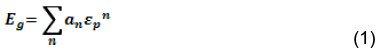
Now we are going to present the results of the tight-binding calculation for the three main gaps in the form of suitable interpolations. The functional variation of the main energy gapswith the in-plane strain can be fitted --in each case-- to polynomial dependences of the general type (in units of eV):
As it was seen in I, the results for the fitting coefficients, an, need to be given separately for negative and positive deformations. This is due to the difference in the gap functional variations in both intervals. These coefficients are reported in Table 1.
It is observed that the results of some of the fittings lead to high polynomial orders (fourth or higher) in the functional dependencies upon the in-plane deformation, mainly in the case of the Γ-related energy gap. It can be seen from figures 6 (7, 8, 9, 10) to 11 that even for lines which seem to represent a linear behavior, there is in fact a quadratic or a cubic one. This means that such variations resemble a strong non-linear character. Although not directly related to the uniaxial strain direction studied in this article, or with the materials considered here, we can mention recent reports addressing nonlinearities in electronic or elastic properties of semiconductors under some kind of deformation. For instance, we have the work by Bouhemadou et al. on the hydrostatic pressure effects on the elasctic properties of III-P semiconductors [Bouhmadou 2009]. Also, there is a report on the non-linear [111]-strain-induced variation of the electron effective mass in degenerately doped n-Si [Shenderovskii 2009].
Such kind of non-linear variation of the effective mass is shown as an example in figure 12. There one finds the plottings of both obtained points and polynomial fittings for some of the calculated effective masses. The strongly non-linear dependence of the Γ-related [111] conduction band effective mass is clearly observed. Special consideration is deserved by the situations of band inversion detected in the cases of GaSb and InSb. It can be seen that at the very point of inversion the effective mass undergoes a steeped increasing compared with the decreasing tendency exhibited for in-plane deformation values immediately below Above this point m*Γreturns to values around those presented when εp ≤ εpinv ; but, then, an increasing variation starts to reveal.
Up to the authors's knowledge, there are not reports in the scientific literature regarding experimental studies on the [111] uniaxial strain effects on the electronic properties of the III-V semiconductor materials investigated in this work. Even for much more studied materials like GaAs and GaP, only very recent and very scarce research communications can be found [Grivickas 2007, 2009]. Perhaps the only exception in this sense is the theoretical study on deep levels performed by Jenkins et al. [Jenkins, 1989].
For that reason, and viewing the somewhat surprising results of the present study, we consider that this subject deserves to be much intensely investigated both theoretically and experimentally. We consider that the subject the tight-binding investigation of non-linear variation of effective masses as functions of uniaxial strain has its own particular interest and, due to the extension of the present article, it will be presented in a third part of this study, in which both conduction and valence effective masses will be analyzed for the nine III-V zincblende semiconductors considered.
Conclusions
In this work we have performed a tight-binding calculation of the electronic properties of some zincblende III-V materials: AlP, InP, AlSb, GaSb, and InSb. In particular, we analyze the influence of uniaxial strain along the [111] crystal axis. Effects of the strain on the energy dispersion relations in the main Brillouin zone directions are discussed, and a strain-induced band inversion phenomenon is detected in the cases of the narrow gap GaSb and InSb
Our results provide information that may be useful to those performing studies on the electronic properties of [111] strained heterostructures within the effective mass approximation (EMA), involving the materials studied here. For that reason, we present the outcome of polynomial fittings representing the variation -as functions of strain- of some important input parameters of the EMA modeling: energy gaps and electron effective masses.
Acknowledgements
MEMR acknowledges support from Mexican CONACYT through grant CB-2007-80846, and from UAEMor through PROMEP-2009 grant "Proyectos Individuales para la Generación y Aplicación Innovadora del Conocimiento".
References
Bassani, F., and G. Pastori Parravicini. (1975). "Electronic States and Optical Transitions in Solids'". Pergamon Press, Oxford. [ Links ]
Bennett, B. R., R. Magno, J. Brad Boos, W. Kruppa, and M. G. Ancona. (2005). Sol. Stat. Electron. 49, 1875. [ Links ]
Bir, G. L., and G. E. Pikus. (1974). In "Symmetry and Strain-Induced Effects in Semiconductors". John Wiley, New York. [ Links ]
Bouhemadou, A., R. Khenata, M. Kharoubi, T. Seddik, A. H. Reshak, and Y. Al-Douri. (2009). Comput. Mater. Sci. 45, 474. [ Links ]
Boykin, T. B., G. Klimeck, R. C. Bowen, and F. Oyafuso. (2002). Phys. Rev. B 66, 125207. [ Links ]
Chow, D. H., Y. H. Zhang, R. H. Miles, and H. L. Dunlap. (1995). J. Cryst. Growth 150, 879. [ Links ]
De Dios-Leyva, M. and J. López-Gondar. (1985). phys. stat. sol. (b) 128, 575. [ Links ]
Dimmock, J. O., I. Melngailis, and A. J. Strauss. (1966). Phys. Rev. Lett. 16, 1193. [ Links ]
Grivickas, P., M. D. MacCluskey, and Y. M. Gupta. (2007). Phys. Rev. B 75, 235207. [ Links ]
Grivickas, P., M. D. MacCluskey, and Y. M. Gupta. (2009). Phys. Rev. B 80, 073201. [ Links ]
Jancu, J.-M., R. Scholz, F. Beltram, and F. Bassani. (1998). Phys. Rev. B 57, 6493 (1998). [ Links ]
Jancu, J.-M., P. Voisin. (2007). Phys. Rev. B 76, 115202. [ Links ]
Jenkins, D. W., S. Y. Ren, and J. D. Dow. (1989). Phys. Rev. B 39, 7881. [ Links ]
Li, E. H. (2000). Physica E 5, 215. [ Links ]
Martínez, G. (1973). Phys. Rev. B 8, 4678. [ Links ]
Mora-Ramos, M. E. and J. J. Martín Mozo. (2009). Nova Scientia 2, 66. [ Links ]
Milanović, V., D. Tjapkin. (1982). phys. stat. sol. (b) 110, 687. [ Links ]
Muramatsu, S. and M. Kitamura. (1993). J. Appl. Phys. 73, 4270. [ Links ]
Niquet, Y. M., D. Rideau, C. Tavernier, H. Jaouen, and X. Blase. (2009). Phys. Rev. B 79, 245201. [ Links ]
Sarney, W. L., L. Salamanca-Riba, J. D. Bruno, and R. L. Tober. (2002). Sol. Stat. Electron. 46, 1643. [ Links ]
Shenderovskii, V., V. Baidakov, S. Budsuliak, A. Gorin, V. Ermakov, V. Kolomoets, E. Liarokapis, G. Gromova, B. Kazbekova, and L. Taimuratova. (2009). phys. stat. sol. (b) 246, 612. [ Links ]
Schets, H., P. Janssen, J. Witters, and S. Borghs. (1999). Sol. Stat. Comm. 110, 169. [ Links ]
Scholz, R., J.-M. Jancu, F. Beltram, and F. Bassani. (2000). phys. stat. sol. (b) 217, 449. [ Links ]
Strauss, A. J. (1967). Phys. Rev. 157, 608. [ Links ]
Vurgaftman, I., J. R. Meyer, and L. R. Ram-Mohan. (2001). J. Appl. Phys. 89, 5815. [ Links ]

