


Servicios Personalizados
Revista
Articulo
 Inglés (pdf)
 Artículo en XML
 Referencias del artículo
 Enviar artículo por email
Indicadores
-
 Citado por SciELO
 -
 Accesos
Links relacionados
-
 Similares en
SciELO
Similares en
SciELO
Compartir

 Permalink
Nova scientia
versión On-line ISSN 2007-0705
Nova scientia vol.2 no.3 León abr. 2010
Ciencias Naturales e Ingenierías
Electronic Properties of III-V Semiconductors under [111] Uniaxial Strain; a Tight-Binding Approach: I. Arsenides and Gallium Phosphide
"Propiedades electrónicas de semiconductores III-V sometidos a tensión uniaxial en la dirección [111]; un enfoque según el método tight-binding: I. Arseniuros y Fosfuro de Galio"
Miguel E. Mora-Ramos 1 y J. Juan Martín Mozo2
1 Facultad de Ciencias, Universidad Autónoma del Estado de Morelos. Cuernavaca, Morelos. México.
2 Centro de Investigación en Dispositivos Semiconductores-ICUAP, Benemérita Universidad Autónoma de Puebla. Puebla. México.
Miguel E. Mora-Ramos. E-mail: memora@uaem.mx
Recepción: 07-09-09
Aceptación: 14-10-09
Abstract
The sp3s*d5 empirical tight-binding approach is used to study some properties of the electronic structure in a group of III-V zincblende semiconductors which are of most intersest to electronics and optoelectronics. Particularly, it is investigated the influence of [111] uniaxial strain upon these properties. We make use of a formulation based on the elasticity theory to properly derive the relative positions of the nearest neighbors in the lattice and, consequently, write down the set of four basis vectors centered at the anion. Special attention is paid to the inclusion of the internal deformation effect. We present the variation of the Γ-, X- and L-related energy gaps and conduction band effective masses as functions of the uniaxial strain in the case of AlAs, GaAs, InAs, GaP. Comparison with experimental reports on indirect interband transitions in bulk GaP under compressive strain gives very good agreement between these reports and the calculated variation of X-related energy gap as a function of the strain.
Keywords: tight-binding, III-V materials, electronic structure, uniaxial strain.
Resumen
Empleando un esquema de cálculo tight-binding que usa una base de orbitales sp3s*d5 , se estudian propiedades de la estructura electrónica de un grupo de materiales semiconductores III-V los cuales son de notable interés para la tecnología de dispositivos electrónicos y optoelectrónicos. En específico, se analiza la influencia sobre estas propiedades de una tensión aplicada según la dirección cristalográfica [111], haciendo uso de una formulación basada en la teoría de la elasticidad para establecer las posiciones relativas de los iones vecinos más próximos. Especial atención se presta a la inclusión del efecto de deformación interna de la red cristalina. Para cada material de los estudiados presentamos las dependencias de las brechas energéticas asociadas a los puntos Γ, X y L de la zona de Brillouin como funciones de la tensión uniaxial en AlAs, GaAs, InAs y GaP. Asimismo, reportamos expresiones de ajuste para los valores de las masas efectivas de conducción en esos cuatro materiales. La comparación de la variación de la brecha de energía en X para el GaP, calculada con nuestro modelo, y recientes resultados experimentales para la transición indirecta entre la banda de huecos pesados y la banda X de conducción arroja una muy buena concordancia.
Palabras Clave: tight-binding, materiales III-V, estructura electrónica, tensión uniaxial.
Introduction
The large number of applications of semiconductor hetero- and nanostructures stimulate a non-decaying interest in the study of fundamental physical properties of these systems. Among them, strained layer structures have the additional interest of enlarging the range of potential applications, because of the great influence of built-in strains on the electronic structure of the systems, specially for states near the energy band gap. This encompasses a rich phenomenological variety which makes strained layer systems very interesting [Osbourn 1986, Smith 1990].
The effect of strain on electronic states in semiconductors has received considerable attention for more than 5 decades up to the present time. Different kinds of optical measurements have been used to determine the shifts due to strain as well as the splittings of the band extrema [see Cardona 1999, and references therein]. Among the theoretical approaches used to study the influence of strain on the electronic properties of zincblende crystals we can mention early calculations in GaAs using the Ceperley-Alder description of the local-density approximation with relativistic corrections [Christensen 1984]. The purpose of that work was to calculate -mainly- the strain dependencies of conduction band properties, due to the inaccuracy in the values for the energy gaps obtained within such a calculation procedure. Throughout these years, the band gap problem of density functional theory in the local density or generalized gradient approximations has been a limitation in the obtention of accurate relations involving energy gaps and strain in semiconductors when using this variant of first principle calculations. Things are likely to be changing in this direction with the introduction of the so-called hybrid functional [Heyd 2003,2006] which allows to overcome the deficiencies above mentioned. Very recently, this formulation was applied to study the strain effect in group-III nitrides [Yan 2009].
The empirical tight-binding scheme is a cheap and rather accurate method of calculation of the electronic structure in bulk semiconductors. It is quite readily extended to deal with electronic states in semiconducting heterostructures [García-Moliner 1992, Yan Voon 1993]. On the other hand, the parametrizations that this method involves are in many cases fitted to experimental values or to results outcoming from another first-principles approaches which do not suffer of deficiencies in giving correct values for the energy gaps.
The use of a sp3s*d5 basis set to perform tight-binding (TB) calculations of the electronic structure in semiconductors has some precedents in the literature [Richardson 1986, Chang 1990]. The semiempirical TB sp3d5 Hamiltonian with first nearest neighbors, in the case of Si, was given in [Ren 1997].
The empirical sp3s*d5 TB method for tetrahedrally coordinated group-IV and III-V (non-nitride) cubic materials that incorporated all five d orbitals per atom in the basis set was put forward by Jancu and collaborators for nearest-neighbor interactions [Jancu 1998]. It carefully reproduces ab initio pseudoptential calculations and experimental results of bulk semiconductors. For a detailed discussion of the advantages of the method and an extension of it to the study of electronic states in semiconducting heterostructures the reader is referred to the paper by Scholz et al. [Scholz 2000]. On the other hand, Boykin and collaborators included interactions up to second-nearest-neighbor, and thus more parameters [Boykin 1999]. Later on, this approach was extended to calculate the band structure in both zincblende and wurtzite III-V nitrides [Jancu 2002]. Among the advantages of the inclusion of d orbitals (with just first nearest neighbors) we can mention the obtention of a quantitatively correct description of the valence bands and the two lowest conduction bands both in terms of energy values and band curvatures. It also gave the correct size and the magnitude of the deformation potential of the conduction band at the X point, which is directly related to the large d component of the wave function. The method has been also applied to the calculation of zero-field spin splittings in GaSb/AlSb quantum wells [Jancu 2004], as well as for the determination of a new k•p parametrization in non-nitride III-V semiconducting materials [Jancu 2005]. In addition, it has been shown that the strain-induced splittings of the on-site energies of p and d orbitals are of utmost importance in the obtention of the deformation potentials in zincblende semiconductors [Jancu 2007]. The surface band structure of anion terminated ideal (001) surfaces in zinc-blende AlN, GaN and InN has also been a subject of study [Mora 2006]. In all cases it has come out that for III-V materials crystallizing in the zinc-blende phase, the empirical sp3s*d5 nearest neighbors model gives the possibility of get rid of the complications of incorporating the interactions between second nearest neighbors as well as the limitations posed by the use of smaller TB Hamiltonians.
The electronic properties of a solid are significantly modified due to a deformation of its crystalline structure. Application of a certain strain to the crystal will -in general- result in a variation of the interatomic distances as well as of the bond angles. As a consequence, the energy spectrum modifies in such a way that important features like energy gaps and effective masses are changed. Within this context the sp3s*d5 empirical TB theory has seen modifications in the form of the incorporation of general distortions in such a way that the local strain variations present in nanoscale structures can be dealt with. This is due to the failure of the methods and parameterizations that are typical in the approaches used to describe the effects of uniaxial strain or hydrostatic pressure. In this sense it can be mentioned the method that shifts the diagonal Hamiltonian matrix elements due to the displacements of neighboring atoms [Boykin 2002]. More recently, a model for the on-site matrix elements of the sp3s*d5 TB Hamiltonian in strained diamond or zinc-blende crystal and nanostructures has been proposed [Niquet 2009]. This model generalizes Jancu et al.'s approach by introducing strain-dependent coupling matrices between the s and s* orbitals with p and d orbitals; between the p orbitals, and between the d orbitals, as well as the corresponding couplings between the p and d orbitals.
In this article and in the subsequent one we are interested in studying some properties of the electronic structure of the non-nitride zincblende semiconductors -AlP, GaP, InP, AlAs, GaAs, InAs, AlSb, GaSb, and InSb- in the situation in which there exists a strain along the [111] crystal direction. These materials have been combined to form strained semiconducting heterostructures. To illustrate this we just mention a few examples: GaAs/GaP superlattices were investigated by Dandrea and Zunger [Dandrea 1991], and some studies on strained InAs/AlAS superlattices are reported quite recently [Caha 2005]. On the other hand, [111]- oriented lattice-matched GaAs/AlAs superlattices have also been considered in several works [Xia 1990, Ikonić 1992]. Together with all this there have been numerous reports on the strained InAs/GaAs heterostructures, due to their prospective applications in optoelectronics (see, just for instance, refs. [Magri 1990, Kim 2002, Pearson 2004, Piquini 2008]), whereas a tight-binding approach was presented for the study of strain effects in strongly coupled self-assembled InAs/GaAs quantum dots [Jaskolski 2006].
In many studies involving strained heterostructures, the envelope function approximation is the mathematical tool of choice for calculating electronic properties. Within this context, the knowledge of the effective masses and energy gaps and their variations with strain are of the upmost importance. Our aim here is to provide information regarding those properties in the case of the III-V zincblende semiconductors, taking into account the influence of uniaxial strain applied along the [111] crystal direction. We are therefore interested in the possibility of deriving analytical expressions for such quantities as functions of strain. With this purpose, we adopt the more classical approach of modifying the TB empirical Hamiltonian by means of appropriate changes in the director cosines and the interatomic distances, keeping the parameterizations originally reported by Jancu et al. [Jancu 1998]. This study can directly lead to the investigation of the electronic states in [111] -oriented III-V zinc-blende superlattices and quantum wells by using the tight-binding surface Green function matching method (TB-SGFM). Antecedents on this kind of calculation using sp3s* orbitals are reported for [100] superlattices for the GaP/GaAs [Arriaga 1991-I] and the AlAs/InAs systems [Arriaga 1991-II]. TB-SGFM results for the conduction and valence band states in zinc-blende [001] GaN/AlN quantum wells were put forward using sp3s*d5 parameterizations [Velasco 2007].
Given the discussion above, the first part of the present work is devoted to present a TB study of the four materials which has attracted the greatest interest for the design and fabrication of strained semiconducting nanostructures: AlAs, GaAs, InAs, and GaP. The article is organized as follows. Section 2 is devoted to present some particular features of the model. Section 3 contains the results and discussion and, finally, section 4 presents the conclusions of the work.
Model
Strain-induced atomic rearrangement implies a modification of the matrix elements of the empirical TB Hamiltonian. Angular variation is then taken into account via the changes of the directing cosines. The variation in the distance between atoms is empirically introduced into the Hamiltonian elements by means of a scaling law of the form 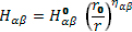 where
where  are the unstrained Hamiltonian matrix elements,
  is the scaling factor in which r0 is the unstrained interatomic distance. On the other hand, r is the value of such distance when there is a deformation [Harrison 1980]. The exponents ηαβ can depend upon the specific pair of atomic orbitals {α,β}, as it was pointed out in Ref. [Priester 1988].
It is possible to understand the effect of the application of uniaxial strain along a certain symmetry direction if we take into account that it is equivalent to apply a biaxial strain upon a plane that is perpendicular to that particular axis. Then, the detail in the [111] case is that the in-plane deformations must be considered equal, that is; ε11 = ε2z = εp.
To study the effect of this particular strain, the system of axes is subject to a rotation in such a way that the z-axis of the rotated system coincides with the [111] direction of the non-rotated system. Taking in both cases the origin of coordinates to be located at the anion, the positions of the 4 nearest-neighbor cations  transform under the rotation into the vectors
  (¡=1,2,3,4). The transformation matrix for this change of cation coordinates is:

On the other hand, the deformations εij can be determined from the generalized Hooke's Law:
Tαβ + Cαβklεkl = 0. with Tαβ = 0, for the values (αβ)=(33),(23),(13), one obtains ε12 =ε13 = ε13 = 0. Additionally, making ε33 = ε⊥ we have:

The generalized Poisson ratio in the rotated frame can be written as:

Meanwhile, the transformed elastic constants are given by:
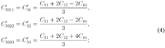
where the abbreviated notation has been used. In terms of the elastic constants C11, C12, and C13, the Poisson ratio in the [111] direction and the connection between the uniaxial deformation ε⊥ and the in-plane one are now obtained in the form:

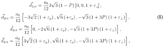
The application of a strain along the [111] direction has also the consequence of a relative displacement of the anion and cation sublattices of the zincblende structure. This results in an internal displacement within the unit cell which is characterized by the so-called Kleinman parameter, ς [Kleinman 1962]. In our particular case, the internal displacement is represented by the vector,

It is defined by taking the origin of coordinates at the position of the anion atom. In this expression, the quantity α0 represents the lattice constant. The values of ς used in this work, for the different materials studied are taken to be those derived in Martin's theory [Martin 1970], and they are listed in the work by Muramatsu et al. [Muramatsu 1993].
The effects of strain upon a given system can be understood if the changes it induces over the unitary directing vectors are specified. In the particular situation of the [111] direction we have:

The vector positions referred to the -unstrained- [100] direction are: (1,1,1), (-1,-1,1), (1,-1,-1), and (-1,1,-1), while the the rotated ones (obtained from the multiplication using matrix M given in equation (1)) are: 
Meanwhile, the combined use of equations (6) and (7) leads us to the definitive working basis vectors, incorporating rotation, strain and internal deformation:
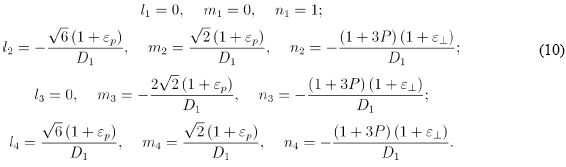
Finally, directing cosines can be obtained with the use of above equations, and defining:

Then, the corresponding directing cosines for the four basis vectors are:
Including spin-orbit effects, the sp3s*d5 is a 40-band model. Details of the Hamiltonian matrix elements are found, for instance, in the work by Yan Voon (Appendix C) [Yan Voon 1993].
Results and discussion
The next step in the process is the diagonalization of the sp3s*d5 TB matrix Hamiltonian constructed for the strained basis [Vogl 1983, Priester 1988]. The corresponding nearest neighbor Slater-Koster parameters for the considered materials are extracted from Ref. [Jancu 1998].
Figures 1 to 5 (2, 3, 4)show the [111] dispersion relations of the upper three valence bands and the lower two conduction bands along the L→Γ and Γ→X directions in the Brillouin Zone. They correspond to AlAs, GaAs, InAs, and GaP.

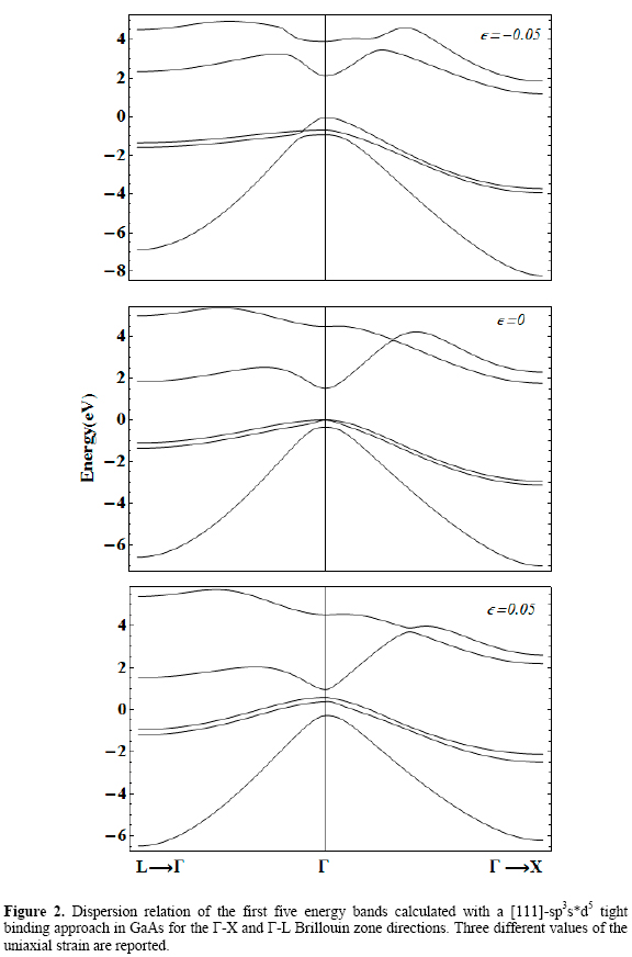
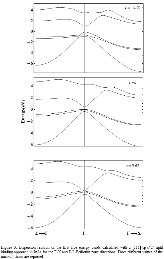


Three different values of the [111] strain, εp, are considered, including the zero strain case. They are taken going from -5 % (compressive in-plane deformation) to 5 % (tensile in-plane deformation), except for the case of InAs in which positive strain up to only 2 % is considered for reasons that will be discussed below.
It is readily seen that strained crystals show significant differences in their electronic structure compared to the unstrained ones.
In general, the influence of a [111] uniaxial strain on the first conduction band zone center edge can be resumed as: Compressive strain tends to shift this minimum upwards while tensile strain shifts it downwards. The strength of the shifting is larger in the case of tensile deformation, although its magnitude depends on the specific material.
In particular, the first two conduction bands calculated using a basis with d orbitals show a kind of anti-crossing at certain curvature-inversion point, not appearing in the sps* results [Vogl 1983, Priester 1988]. The effect of strain over this feature is different depending on the sign of the in-plane deformation. For εp <0 it tends to disappear, whilst in the case of εp >0 it is kept, but its position along the Γ→X shifts towards the X point.
The analysis of the valence band spectra shows that, in general, the effect of the strain is to eliminate the heavy- and light-hole zone-center degeneracy, as it should be expected. However, besides this effect some particularities can be discussed. In first place, the general consequence of a negative in-plane deformation is to enhance the separation between heavy- and light-hole bands at the Brillouin zone center. The tendency is to slightly shift down the heavy hole band and to significantly shift down both light hole and split-off bands although these two remain close each other. In order to elucidate the origin of the -apparent- accidental degeneracy occurring between heavy and light hole bands in the Γ→L direction of the band structure of GaAs, AlAs, and InAs under compressive strain, it is shown in figure 4 an enhanced picture of the dispersion of those energy bands. We have chosen the case of GaAs as an example. Then, it is observed that what we really have is an anticrossing of both bands. Negative values of wavevector modulus have been used only for graphical convenience, to coherently match with figure 2 layout.
In addition, figure 6 shows the same enhancement in the case of GaP. Although it is apparent from the dispersion energy band graphics of figure 5 that there would be some kind of interband interaction involving hole split-off band, it is shown that it is, in fact, present. There is only the same kind of HH and LH anti-crossing exhibited in the III-V arsenides. Additionally, both in the cases of 5% negative (Γ→X, and Γ→L) and positive strain (Γ→L), the proximity of hole bands detected in figure 5, does not correspond in any case to an interband interaction.

Enhancing the graphics shows that in those situations hole bands remain in practice, almost parallel.
On the other hand, the influence of a positive strain reveals in the form of a significant shift upwards of the heavy- and light-hole bands at the Γ-point, keeping a relatively small energy difference between them. At the same time, the split-off band edge at that point moves considerably downwards. The result is an enhancement of the separation between the position of the split-off band maximum and the corresponding one of the light-hole one.
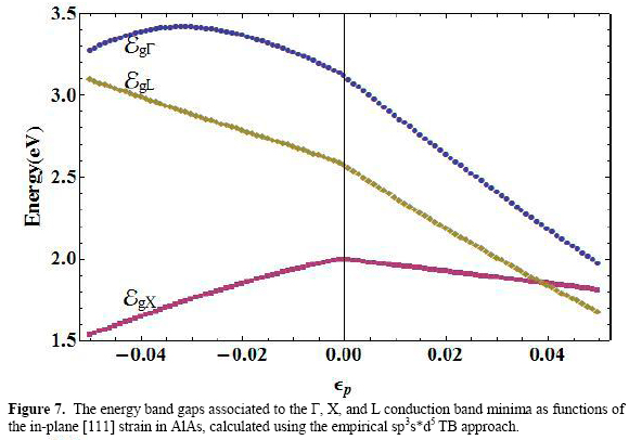
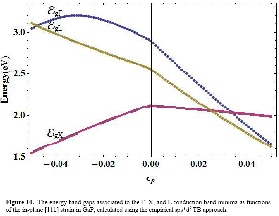
For a separate discussion of the variation of the main energy gaps in the four materials figures 7, 8, 9, and 10 show, in AlAs, GaAs, InAs, and GaP respectively, the behaviors of these quantities for the Γ (EgΓ), X (EgX), and L (EgL) points of the Brillouin zone, measured with respect to the top of the corresponding valence band at the zone center.


It is necessary first to properly analyze the situation observed in the case of InAs. As it can be seen, for tensile strains larger than 0.02 the variation of the gaps in this material is not reported. The explanation for this decision follows the results presented in figure 3. There it is shown that for this value the InAs turns into a zero gap material.
That is, the effect of such uniaxial strain is to induce a transition to a semimetal, and above that value our calculation leads to an inversion of the conduction and top valence bands. Thevery sense of the Γ-point related energy gap is lost. Presumably, what we will be faced with in this situation is not only an electronic phase transition but also a structural one.
In consequence, it is apparent that the results obtained for values of positive strain beyond the transition threshold can not be trusted for the calculation approach itself fails in its presumptions.
Among the three gaps, the Γ-point-related exhibits a homogeneous decreasing variation in the the whole range of strain for the cases of GaAs and InAs. Nonetheless, the functional form of this variation is different whether the strain is negative or positive.
For AlAs and GaP there appears a narrow region between εp= -0.05 and εp= -0.04 in which EgΓ goes upward, and then becomes a decreasing function as compressive strain diminishes in magnitude, for the entire range of tensile deformation. The value εp= 0 serves as an inflexion point of the energy gap function. This particular role of null strain as a delimiter of the shape of the energy gap curve as a function of εp is common to the three main gaps.
The null strain value becomes the maximum for EgX (εp) in the four materials. This feature is more pronounced in the case of the X-related energy gap. As shown in the figures, the functional dependence EgX has a decreasing character for tensile strain and increases as long as the compressive strain magnitude falls to zero.
Finally, the function EgL (εp) exhibits a mixed behavior depending on the material. For GaP and InAs the form of the curve is similar to those at X-point (with a maximum in εp=0). A monotonically decreasing variation is observed for this function in GaAs and AlAs.
The functional variation of the main energy gaps with the in-plane strain can be fitted -in each case- to polynomial dependences of the general type (in units of eV):

The results of our calculation for the [111] energy gaps show that it is not much convenient to try fitting the obtained energies over the entire range of strain. This is because it would involve quite cheap higher order polynomial approximations. Instead, we have decided to split the functional dependence into two different parts. One of them will correspond to the compressive strain and the other to the variation of the energy gaps with the tensile strain. In general, it has been possible to fit the gaps in the form of second or third order polynomials.
Considering first the polynomial fittings associated to the region in which εp <0, for the Γ-point energy gap we have the following coefficients of the expansion (11): α0 =3.13, a1 = -13.44, α2 =4301.81 (AlAs); α0 =1.52, a1 =-17.90, α2 =-10.99, α3 =1057.75 (GaAs); α0 =0.41, α1 =-13.68, α2 =-465.80 (InAs), and α0 =2.89, α1 =-16.27, α2 =-108.18, α3 =3209.15 (GaP).
For εp <0, the fitting of the [111] X-point energy gap has the coefficients given by: α0 =2.00, α1 =6.65, α2 =-56.39 (AlAs); α0 =1.76, α1 =7.06, α2 =-103.36, α3 =-641.40 (GaAs); α0=1.93, α1=5.78, α2 =-59.36, α3=-417.24 (InAs), and α0=2.12, α1=8.77, α2 =-84.48, α3=-631.88 (GaP).
In the same strain region, the coefficients corresponding to the expansion of EgL are: α0 =2.57, α1 =-11.22, α2 =-54.09, α3 =-769.18 (AlAs); α0 =1.84, α1 =-10.62, α2 =-38.75, α3 =-759.64 (GaAs); α0 =1.68, α1 =7.58, α2 =-9.08, α3 =-636.70 (InAs), and α0 =2.56, α1 =-10.19, α2 =-20.38, α3=-728.35 (GaP).
We now present the polynomial fittings of the form (11) in the case of tensile strain. Notice that in the case of InAs, these expressions are restricted to the condition εp ≤ 0.02.
Starting again with EgΓ we have: α0 =3.13, α1 =-25.09, α2 =40.56 (AlAs); α0 =1.52, α1 =-26.84, α2=73.36 (GaAs); α0=0.41, α1=-20.39, α2 =5702.69 (InAs), and α0=2.89, α1 =-26.72, α2 =23.11, α3 =363.21 (GaP).
The coefficients of (11) for EgX (εp >0) are: α0 =2.00, α1 =-3.54, α2 =-3.47 (AlAs); α0=1.76, α1=-2.95, α2 =0.53, α3=-92.55 (GaAs); α0=1.93, α1=-3.06, α2= -34.60, α3= 711.05 (InAs), and α0=2.12, α1=-2.29, α2 =-6.28 (GaP).
Finally, the [111] gaps at the L point of the Brillouin zone for positive strain are fitted to (11) with the help of the coefficients: α0=2.57, α1=-20.29, α2 =46.48 (AlAs); α0=1.84, α1=-20.63, α2=64.44, α3 =-177.48 (GaAs); α0=1.68, α1=-16.39, α2 =44.08 (InAs), and α0=2.56, α1 =-21.15, α2 =52.04 (GaP).
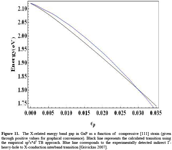
Experimental reports on the variation of the main energy gaps with [111] uniaxial strain in bulk III-V arsenides and GaP are very scarce. Most works studying the effect of such kind of deformation on the electron energy spectrum deal with III-V-based heterostructures. However, very recently, shock compression experiments have been performed to investigate optical changes involving indirect band-gap transitions in GaP [Grivickas 2007]. Figure 9 shows the comparison of the indirect X-related energy gap for this material, calculated with our model and the experimentally determined transition between zone-center-heavy-hole to X-conduction bands, as functions of compressive strain given in that work. The variation of strain is restricted to an upper value of 3.5%, to match the reported experimental range.
It can be seen that our calculation reproduces correctly the decreasing behavior of this main energy gap in bulk GaP for increasing compressive [111] uniaxial strain. The quantitative difference between experimental and calculated results does not surpass the amount of 20 meV along the entire range of strain considered. This represents about 1%, and may lie within the range of experimental uncertainty although this is not reported in the work by Grivickas et al.
Theoretical works regarding uniaxial strain in bulk semiconductors have dealt mainly with [100] and [110] strain directions [see Christensen 1984 and Cardona 1996], whilst the [111] uniaxial strain has been mainly studied in heterostructures.
Up to the authors's knowledge, no other calculations of the variation of energy gaps as functions of [111] uniaxial strain are currently available in the literature -perhaps avoiding the difficulties of density functional schemes- for the materials here considered.
The calculation of [111] electron masses in the conduction band of these four III-V zincblende materials was carried out taking into account the effective variation with the strain of the lattice constant along the [111] direction. For small deformations, this dependence is taken to be of the form:
where α represents the unstrained lattice constant.
The results for the effective masses were also fitted by means of a polynomial form:
m* = Ybn Evn
r - . (13)
In this case, it has been possible to fit the variation in such a way that the information of both negative and positive strain is collected in a single polynomial expression for each conduction band minimum. Then, the outcome for these quatities is shown in Tables 1, 2, and 3.

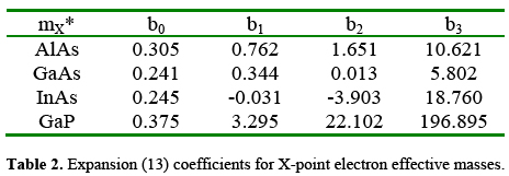

It is possible to verify that our results for zero strain conduction effective masses are in good agreement with previously reported results [Jancu 1998]. Nonetheless, it is important to stress that we are reporting effective masses calculated along the [111] direction. Thus, some slight differences may be detected when comparing with reports of calculations performed along, say, the [100] direction. This is particularly true at the X and L minima, for which the conduction band anisotropy is higher. In these two cases the results correspond to the so-called transversal effective mass. The authors do not know about any previous reports on the sp3s*d5 tight-binding calculation of the electron effective masses in these materials under [111] uniaxial strain.
Although they are quantitatively correct, the results of the fitting are less satisfactory in the case of L-related conduction effective masses. This can be noticed by observing the amount of terms necessary to write polynomial approximations for these quantities in the four materials. The case of GaP turns out to be the more complicated because -besides the need of fourth order polynomials for the Γ and X masses- it requires a sixth order fitting to properly reproduce the results of the TB-based calculations for mtL*. Nonetheless, in the particular case of GaAs, when they are compared with the experimental results our results b0 for the unstrained L-point effective mass provide better agreement than the values reported by Jancu et al. [Jancu 1998]. This gives us confidence in the calculation procedure that writes the TB Hamiltonian according the transformation given by equations (8)-(10).
Conclusions
In this work we have performed a tight-binding calculation of the electronic properties of some zincblende III-V materials: AlAs, GaAs, InAs, GaP. In particular, we analyze the influence of uniaxial strain along the [111] crystal axis. Effects of the strain on the energy dispersion relations in the main Brillouin zone directions are discussed, and a strain-induced transition to semimetal character in InAs is detected above a tensile deformation of 2%.
Our results provide information that may be useful to those performing studies on the electronic properties of [111] strained heterostructures within the effective mass approximation (EMA), involving the materials studied here. For that reason, we present the outcome of polynomial fittings representing the variation -as functions of strain- of some important input parameters of the EMA modeling: energy gaps and electron effective masses.
This is the first part of a more extended work. The sp3s*d5 tight-binding results for the electronic properties of other III-V zincblende materials under [111] uniaxial strain (namely, AlP, InP, and the three antimonides) will be presented elsewhere.
Acknowledgements
MEMR acknowledges support from Mexican CONACYT through grant CB-2007-80846, and from UAEMor through PROMEP-2009 grant "Proyectos Individuales para la Generación y Aplicación Innovadora del Conocimiento".
References
Arriaga, J., G. Armelles, M. C. Muñoz, J. M. Rodríguez, P. Castrillo, M. Recio, V. R. Velasco, F. Briones, and F. García-Moliner. (1991). Phys. Rev. B 43, 2050. [ Links ]
Arriaga, J., M. C. Muñoz, V. R. Velasco, and F. García-Moliner. (1991). Phys. Rev. B 43, 9626. [ Links ]
Boykin, T. B., L. J. Gamble, G. Klimeck, and R. C. Bowen. (1999). Phys. Rev. B 59, 7301. [ Links ]
Boykin, T. B., G. Klimeck, R. C. Bowen, and F. Oyafuso. (2002). Phys. Rev. B 66, 125207. [ Links ]
Caha, O., P. Mikulík, J. Novák, V. Holỳ, S. C. Moss, A. Norman, A. Mascarenhas, J. L. Reno, and B. Krause. (2005). Phys. Rev. B 72, 035313. [ Links ]
Cardona, M. (1996) phys. stat. sol. (b) 198, 5. [ Links ]
Chang, Y. C. and D. E. Aspnes. (1990). Phys. Rev. B 41, 12002. [ Links ]
Christensen, N. E. (1984). Phys. Rev. B 30, 5753. [ Links ]
Dandrea, R. G. and A. Zunger. (1991). Phys. Rev. B 43, 8962. [ Links ]
García-Moliner, F. and V. R. Velasco. (1992). Theory of Single and Multiple Interfaces, Singapore. World Scientific. [ Links ]
Harrison W. A. (1980). Electronic Structure and the Properties of Solids. San Francisco. Freeman. [ Links ]
Heyd, J., G. E. Scuseria, and M. Ernzerhof. (2003). J. Chem. Phys. 118, 8207. [ Links ]
Heyd, J., G. E. Scuseria, and M. Ernzerhof. (2006). J. Chem. Phys. 124, 219906. [ Links ]
Ikonić, Z., G. P. Srivastava, and J. C. Inkson (1992). Phys. Rev. B 46, 15150. [ Links ]
Jancu, J.-M., R. Scholz, F. Beltram, and F. Bassani. (1998). Phys. Rev. B 57, 6493 (1998). [ Links ]
Jancu, J.-M., F. Bassani, F. Della Sala, and R. Scholz. (2002). Appl. Phys. Lett. 81 , 4838. [ Links ]
Jancu, J.-M., R. Scholz, G. C. La Rocca, E. A. de Andrada e Silva, and P. Voisin. (2004). Phys. Rev. B 70, 121306. [ Links ]
Jancu, J,-M., R. Scholz, E. A. de Andrada e Silva, and G. C. La Rocca, Phys. Rev. B 72, 193201. [ Links ]
Jancu, J.-M. and P. Voisin. (2007). Phys. Rev. B 76, 115202. [ Links ]
Jaskólski, W., M. Zieliński, G. W. Bryant, and J. Aizpurúa. (2006). Phys. Rev. B 74, 195339. [ Links ]
Kim, K., P. R. Kent, A. Zunger, and C. B. Geller. (2002). Phys. Rev. B 66, 045208. [ Links ]
Kleinman, L. (1962). Phys. Rev. 128 , 2614. [ Links ]
Magri, R. (1990). Phys. Rev. B 41, 6020. [ Links ]
Martin, R. M. (1970). Phys. Rev. B 1, 4005. [ Links ]
Mora-Ramos, M. E. and V. R. Velasco. (2006). Surf. Sci. 600, 2868. [ Links ]
Velasco, V. R. and M. E. Mora-Ramos. (2007). Surf. Sci. 601, 1079. [ Links ]
Muramatsu, S. and M. Kitamura. (1993). J. Appl. Phys. 73, 4270. [ Links ]
Niquet, Y. M., D. Rideau, C. Tavernier, H. Jaouen, and X. Blasé. (2009). Phys. Rev. B, 79, 245201. [ Links ]
Osbourn, G. S. (1986). IEEE J. Quantum Electronics QE-22, 1677. [ Links ]
Pearson, Ch., C. Dorin, J. Mirecki-Millunchick, B.G. Orr. (2004). Phys. Rev. Lett. 92, 056101. [ Links ]
Piquini, P. and A. Zunger. (2008). Phys. Rev. B 78, 161302. [ Links ]
Priester, C., G. Allan, and M. Lannoo. (1988). Phys. Rev. B 37, 8519. [ Links ]
Ren, S. Y., X. Chen, and J. D. Dow. (1997). J. Phys. Chem. Solids 59, 403. [ Links ]
Richardson, S. L., M. L. Cohen, S. G. Louie, and J. R. Chelikowsky. (1986). Phys. Rev. B 33, 1177. [ Links ]
Scholz, R., J.-M. Jancu, F. Beltram, and F. Bassani. (2000). phys. stat. sol. (b) 217, 449. [ Links ]
Smith, D. L., and C. Mailhiot. (1990). Rev. Mod. Phys. 62 , 173. [ Links ]
Vogl, P., H. P. Hjalmarson, and J. D. Dow. (1983). J. Phys. Chem. Solids 44, 365. [ Links ]
Xia, J.-B. and Y.-Ch. Chang. (1990). Phys. Rev. B 42, 1781. [ Links ]
Yan, Q., P. Rinke, M. Scheffler, and C. G. Van de Walle. (2009). Appl. Phys. Lett. 95, 121111. [ Links ]
Yan Voon, L. C. L. (1993). Electronic and Optical Properties of Semiconductors: A Study based on the Empirical Tight-Binding Model, Boca Raton. Dissertation.com. [ Links ]
Grivickas, P., M. D. McCluskey, and Y. M. Gupta, (2007), Phys. Rev. B 75, 235207. [ Links ]

