


 text new page (beta)
 English (pdf)
 Article in xml format
 Article references
 Send this article by e-mail
 Cited by SciELO
  Similars in
SciELO
Similars in
SciELO 
 Permalink
Introduction
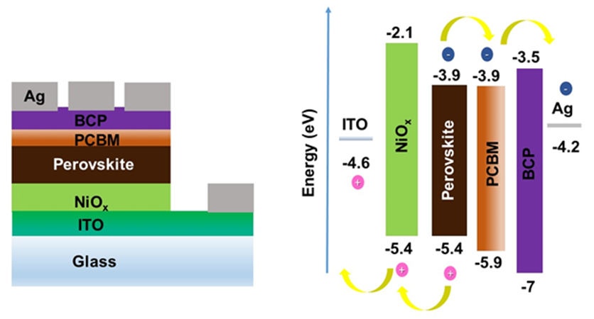
Perovskite solar cells possess great capabilities such as low cost, high power efficiency possessing perovskite materials with long diffusion length, high mobility, tunable band gap, low exciton binding energy, high absorption coefficient [1,2,3,4,5,6,7]. Due to the cost and energy efficient production techniques for fabrication of perovskite solar cells, they are super foreseen as competitors of silicon solar cells [8,9] and are regarded as coming alternatives of silicon-based solar cells [8,10,11]. Perovskite solar cells can be fabricated in two different configurations of n-i-p or p-i-n. n-i-p configuration consists of an electron transport layer (ETL), perovskite semiconductor material, and a hole transport layer (HTL) whereas in the p-i-n, which is also regarded as inverted type perovskite solar cells, a hole transport layer, perovskite layer and an electron transport layer are employed. P-i-n structures serve several advantages such as lower processing temperatures and the use of well-known fullerenes as electron transport layers [12,13,14]. In the p-i-n structure, nickel oxide (NiOx) received very much attention among researchers since NiOx provides good stability and possesses high hole mobility [15-16]. Generally, buffer layers such as bathocuproine (BCP) [17,18,19,20], LiF [21,22], polyethyleneimine (PEIE) [23] are used in p-i-n structure of perovskite solar cells to hinder recombination between ETL and cathode.
Thin BCP films as buffer layers can be processed through vacuum or solution. Although there are various number of studies based on BCP layers processed through vacuum [24,25,26,27], the number of studies on solution processed BCP layers is rather limited [28,29,30,31]. In this work, we studied the effect of BCP layers on the performance of perovskite solar cells by changing the BCP concentration, which was prepared by sol-gel method and also, we have studied the effect of spin-coating speed of BCP layers on the performance of perovskite solar cells in p-i-n configuration as ITO/NiOx/MAPbI3/PCBM/BCP/Ag configuration (Fig. 1) in ambient air under high humidity (~ 60%) conditions. This method, unlike previous ones, does not require a high vacuum system.
Experimental
Materials
PbI2 (lead iodide, Sigma-Aldrich 99.0%), methylammonium iodide (CH3NH3I (MAI), Lumtec 99.99%), Nickel (II) acetate tetrahydrate (Sigma, ≥99.0%), BCP (2,9-dimethyl-4,7-diphenyl- 1,10-phenanthroline, 96%, Sigma), PCBM ([6, 6]-phenyl-C61-butyric acid methyl ester, Solenne, 99%), were purchased and used without further purification.
Device fabrication
124.42 mg nickel (II) acetate tetrahydrate was dissolved in 5 ml isopropanol and 30 µl ethanolamine (MEA) mixture at room temperature. The mixture was stirred at 70 °C for at least two hours to get NiOx solution. This solution is filtered with a 0.22 micrometer PTFE filter prior to spin casting. Perovskite solution was prepared by mixing MAI:PbI2 with a molar ratio of 1.4:1.4 in γ-butyrolactone (GBL) and stirred at 65 °C for at least 6 hours and was filtered with a 0.45 µm PTFE filter. Different concentrations of bathocuproine (BCP) were dissolved in absolute ethanol. PCBM solution was achieved by dissolving 20 mg PCBM powder in 1 ml chlorobenzene (CB) and stirring at room temperature for 2 hours.
For fabrication of devices initially, one-third of ITO coated glasses were etched by a mixture of HCl:HNO3:H2O (4.6:0.4:5) acid solution and were cleaned by ethanol, acetone and isopropanol, respectively. Then they were sonicated separately in acetone (for 20 minutes) and isopropanol (for 45 minutes at 60 °C) to remove any kind of impurities on the surface. Finally, substrates were dried by N2 gas.
NiOx solution was spin coated at 1500 rpm for 30 seconds at room temperature and coated substrates dried at 80 °C on a hot plate for 15 minutes and then coating repeated once more. Finally, NiOx layers were annealed in a muffle furnace at 450 °C for 30 minutes and used without any UV-ozone treatment. Perovskite film was achieved by spin coating the perovskite solution at 2000 rpm for 10 seconds and 4000 rpm for 20 seconds. While the rotation speed approached 4000 rpm, toluene washing was applied to get crystalline perovskite film. Thereafter, thermal annealing at 100 °C for 20 minutes was applied. PCBM solution was cast at 1500 rpm for 30 seconds, then dried at 90 °C for 90 seconds. BCP solutions with different concentrations (0.325 mg/ml, 0.5 mg/ml, 1 mg/ml, 2 mg/l and 4 mg/ml) were spin coated at two different spinning speeds, 1500 rpm and 4000 rpm for 40 seconds, separately. Finally, 110 nm thick Ag was coated by thermal evaporation method.
Characterization
Keithley 2400-LV source meter with LabVIEW software were used for achieving current density-voltage (J-V) curves of devices under illumination of 100 mW/cm 2 to simulate the condition of AM 1.5. Open-circuit voltage (V OC (V)), short-circuit current density (J sc (mA/cm 2 )), fill factor (FF) were determined from J-V curves. Fill factor is given by following formula:
And the power conversion efficiency (PCE) of device was determined by the ratio of power-out to power-in as following formula:
I-V curve of solar cell can be calculated in presence of shunt and series resistance as follow
where, I L is light generated current, I 0 is saturated current, T is temperature, n is ideality factor, R s is series resistance, R sh is shunt resistance, k B is Boltzmann’s constant, and q is electronic charge.
Incident photon to current efficiency (IPCE) was performed with New Port measurement system, which contains optical system consisting of a xenon lamp, a filter wheel, mechanical chopper, and a monochromator. The absorption spectra of perovskite film were achieved by using a Perkin Elmer Lambda 950 UV-VIS spectrometer. Crystalline structure of perovskite layers observed by a PANalytical Xpert PRO MRD X-ray diffractometer. FTIR spectra of the perovskite layer recorded with a Thermo Nicolet 6700 spectrometer. Photoluminescence spectroscopy of perovskite layer was achieved by using PerkinElmer LS 55 Luminescence spectrometer.
Results and discussion
Fig. 2 shows the XRD pattern of the perovskite layer. The peaks refer to characteristic peaks of crystalline perovskite (MAPbI3) structure. 2θ = 13.98°, 28.32° and 31.74°, 40.5° and 42.5° correspond to the (110), (220), (310), (224) and (330) planes, which indicate the formation of the tetragonal perovskite structure [32].
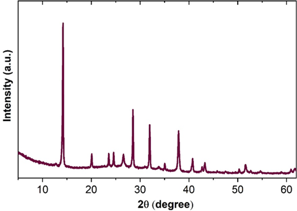
Fig. 3 shows UV-Vis absorption and photoluminescence spectra (PL) of perovskite film. The obtained optical band gap of MAPbI3 is 1.61 eV which is consistent with the reported values [33,34,35].
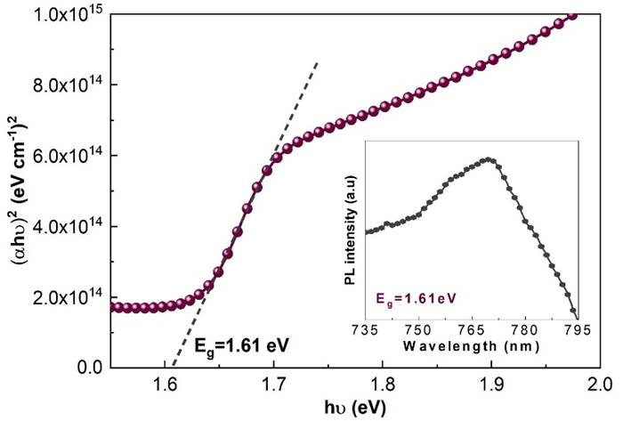
Fig. 4 shows the FTIR spectra of perovskite film coated on ITO substrate. The FTIR spectrum tells about what functional groups present in the molecule. The IR band at 1465 cm -1 is mainly attributed to C‒H band bending in alkane group. The IR band at 3180 cm -1 and 3138 cm -1 belongs to N‒H stretching bond [36-37].
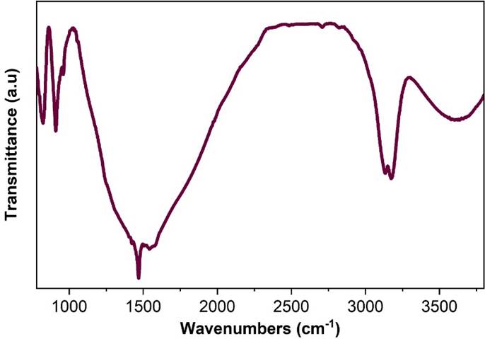
Fig. 5 (a)-(b) shows the current density-voltage (J-V) curves of devices consisting of BCP layers, prepared with different concentrations and spinning speeds of 1500 rpm and 4000 rpm, respectively. The J sc of the devices increased as the concentration of BCP increased to 0.5 mg/ml. As the concentration of BCP is further increased to 2 mg/ml we have observed a reduction in the PV performance of the devices. BCP, Lithium fluoride (LiF) and Ca are widely used in literature as an interfacial layer [38]. They help to prevent the energy mismatch between cathode and electron transport layer and also to prevent the diffusion of cathode to the conducting under-layers, which may lead to recombination [38].
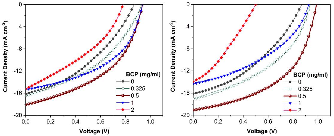
Fig. 5 Current density-voltage curves of the solar cell devices as a function of BCP precursor concentration cast at (a) 1500 rpm and (b) 4000 rpm spinning speeds.
Fig. 6 (a) shows the PCE of the devices with different concentrations of BCP solution cast at 1500 rpm and 4000 rpm. Spin coating is a procedure used to deposit uniform thin films onto flat substrates. Usually a small amount of coating material is applied on the center of the substrate. The substrate is rotated at different speeds to spread the coating material by centrifugal force. Variations in the speed of the spin coating directly affect the thickness of the thin films. Thinner films can be achieved as the spinning speeds are increased. Keeping the BCP concentration constant, we have achieved a higher efficiency when BCP layer is cast at higher spinning speeds of 4000 rpm. Higher spinning speeds lead to thinner films. Therefore, we expect a thinner BCP film for 4000 rpm as compared to 1500 rpm. Please note that the BCP layer is an interfacial layer between ETL and the metal contact therefore if the BCP layer is too thin or too thick, charge accumulation will emerge due to different mechanisms and lead to device performance degradation [39]. We have chosen intermediate low and high spinning speeds as 1500 rpm and 4000 rpm and demonstrated that the 4000 rpm is the proper spinning speed for BCP layers. The devices containing BCP layers cast from 0.5 mg/ml concentration at 4000 rpm exhibit the highest efficiency of all. We have observed that the concentration of BCP solution significantly affected the performance of PSCs. As concentration increased, the power conversion efficiency (PCE) of the PSCs increased at first and then decreased [19].
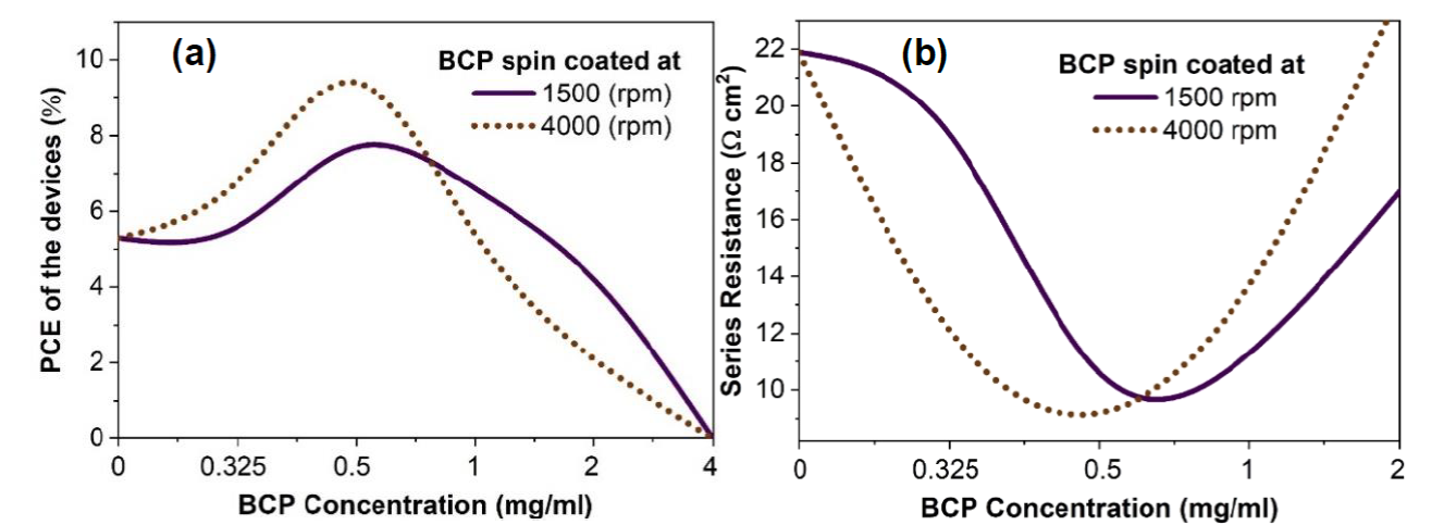
Fig. 6 (a) Power conversion efficiency and (b) series resistance of the solar cell devices as a function BCP layer coating parameters.
Fig. 6 (b) shows the series resistance (R s ) of devices. As can be seen the R s is minimum for devices containing BCP layers with 0.5 mg/ml concentration in both spinning speeds. For devices with no BCP layer, between PCBM and Ag Schottky contact can be formed [40]. Schottky contact causes charge accumulation and large series resistance, which lead to low performance of devices. When a thin layer of BCP is placed between PCBM and Ag, R s is decreased due to formation of an ohmic contact [18]. Thus, the concentration of BCP plays a significant role in the performance of the perovskite devices since viscosity of a solution depends on concentration of dissolved substance [41] and viscosity plays a critical role in thickness of coated film [42]. Due to the insulating feature of BCP, high concentration of BCP could lead to hindering of charge transfer at the interface. It has been observed in literature that too thin or thick BCP layers lead to charge accumulation through different mechanisms, which cause to low device performance [43].
We have fabricated electron-only (e-only) devices in the configuration of ITO/TiO2/Perovskite/PCBM/BCP/Ag and as a comparison we have also fabricated a control e-only device without BCP. Fig. 7 (a) and (b) show the J-V dark J-V characteristics of perovskite solar cells and e-only devices with and without BCP. As can be seen from Fig. 7 (a) , the leakage current density is lower for perovskite solar cells with BCP layer respectively. The leakage current originates from the improper interfacial contact near the contact layer [29] and may reflect the interface condition at some extent. The lower dark current suggests a better interfacial modification by BCP. As can be seen from Fig. 7 (b) , the current increases linearly with voltage up to a kink point. A rise in the current is observed as the voltage is increased above the kink point, which demonstrates the filling of the trap states by injected carriers [44] We have determined the trap densities by using the trap-filled limit voltage (V TFL ) using the equation:
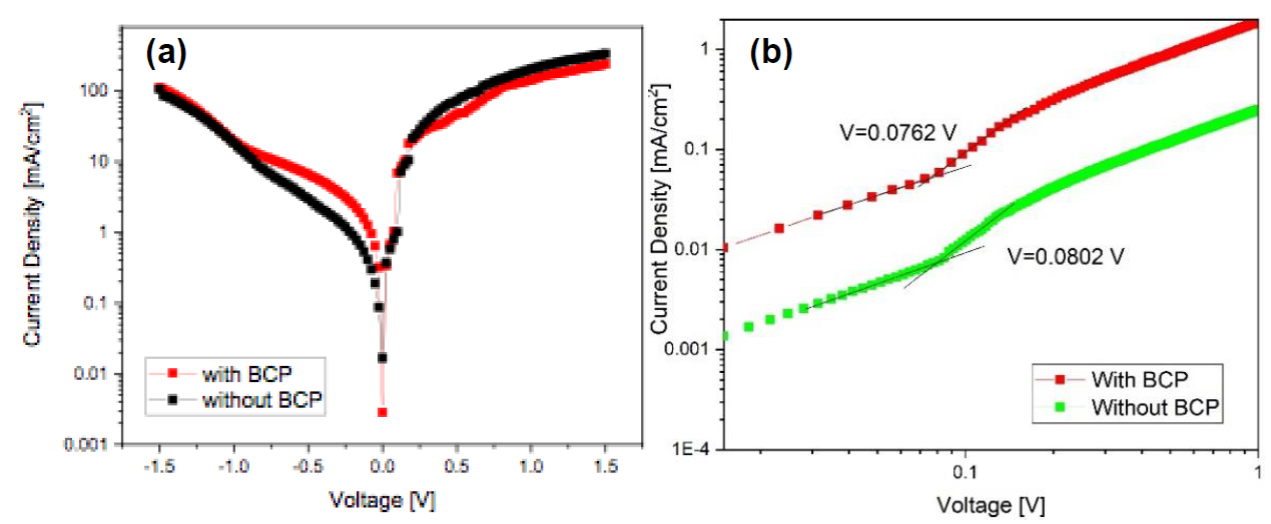
Fig. 7 Dark current density-voltage characteristics of (a) perovskite solar cells (b) e-only devices (ITO/TiO2/MAPbI3/PCBM/BCP/Ag) with and without BCP (0.5 mg/ml, 4000 rpm) layers.
where, n t is the trap-state density, L is the thickness of the perovskite film, e, ε and ε 0 are the elementary charge and permittivity of the perovskite and vacuum, respectively. Dielectric constant of the perovskite was taken as 32 from the literature [45]. The thickness of perovskite layer was240 nm. Trap density was calculated as5.71x10 15 cm -3 for the e-only control device without BCP, whereas trap density was calculated as 4.65x10 15 cm -3 for the e-only device with BCP. As can be seen the trap density is reduced when BCP is introduced in the device configuration, which is an indication of an improved device quality upon BCP addition.
Table 1 presents the photovoltaic parameters of the herein fabricated devices. It can be seen that employing the BCP decreases the series resistance of devices. Devices without using BCP exhibited a J SC of 16.1 mA/cm 2 and a V OC of 0.875 V with a 0.37 of fill factor, which led to a PCE of 5.3 %. The J SC , V OC , and FF increased to 19 mA/cm 2 , 0.99 V, and 0.5, respectively for devices employing BCP layers prepared from 0.5 mg/ml concentration, which led to a PCE of 9.4 %. For higher concentrations, the performance of devices showed a significant reduction in the J SC , V OC , and FF thereby leading to a lower PCE.
Table 1 Photovoltaic parameters of fabricated devices.
| BCP (mg/ml) | Casting (rpm) | VOC (mV) | JSC (mAcm-2) | FF | PCE (%) | RS (Ωcm2) | RSh (Ωcm2) |
|---|---|---|---|---|---|---|---|
| 0 | 875 | 16.1 | 0.37 | 5.32 | 2.19 ×101 | 1.9 × 10² | |
| 0.325 | 1500 | 930 | 16.5 | 0.37 | 5.6 | 1.9 ×101 | 1.65 ×10² |
| 4000 | 930 | 17 | 0.43 | 6.8 | 1.21 ×101 | 1.79 ×10² | |
| 0.5 | 1500 | 930 | 18 | 0.46 | 7.7 | 1.06 ×101 | 1.82 ×10² |
| 4000 | 990 | 19 | 0.50 | 9.4 | 0.92 ×101 | 2.95 ×10² | |
| 1 | 1500 | 930 | 15.3 | 0.47 | 6.6 | 1.13 ×101 | 2.52 ×10² |
| 4000 | 925 | 14.3 | 0.41 | 5.4 | 1.37 ×101 | 2.11 ×10² | |
| 2 | 1500 | 780 | 15.2 | 0.36 | 4.2 | 1.7 ×101 | 8.84 ×10² |
| 4000 | 510 | 13.9 | 0.30 | 2.1 | 2.4 ×101 | 6.88 ×10² |
Fig. 8 shows photovoltaic parameter (V OC , J SC , FF, PCE) statistics of solar cell devices fabricated employing various BCP concentrations at different coating speeds for 15 devices. FF and V OC are related to junction properties of perovskite solar cell [19] and higher V OC and FF enhance the power conversion efficiency (PCE). J SC depends on transferring of generated charge carriers in perovskite layer to the proper transport layer, and if charge carrier transferring does not happen effectively, they will be recombined or accumulated in the interface [46, 47]. As shown in Fig. 7 the current density (J SC ) has been significantly improved along with increasing the BCP concentration to 0.5 (mg/ml). This result illustrates the mentioned concentration of BCP could reduce recombination at interface. Furthermore, the devices exhibit a good reproducibility.
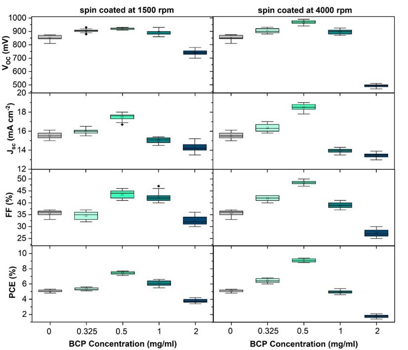
Fig. 8 Distribution of the open circuit voltage, short circuit current density, fill factor and power conversion efficiency values over 15 solar cell devices as a function of different BCP concentrations cast at 1500 rpm and 4000 rpm.
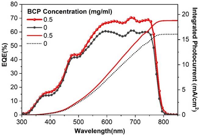
Fig. 9 shows the external quantum efficiency (EQE) of perovskite solar cells with the optimized BCP layer and without BCP layers. EQE is ratio between number of charge carriers generated by photon and collected by device to number of incident photons. Using BCP increased the EQE in both short and long wavelength region. The integrated photocurrent density (J SC ) from the EQE curve was 16.05 mA/cm 2 for PCBM/Ag and 18.7 mA/cm 2 for PCBM/BCP (0.5 mg/ml, 4000 rpm) /Ag. The J SC achieved by EQE spectra were in good agreement with the J SC obtained from J-V measurements. The higher EQE in PCBM/BCP(0.5 mg/ml ) /Ag structure is due to using BCP as a hole-blocking layer which results in reduction in charge carrier recombination at the interface.
Conclusion
In summary, inserting a BCP interfacial layer between the electron transporting layer, PCBM, and the metal contact, Ag improved the performance of perovskite solar cells. The best device performance was achieved when 0.5 mg/ml of BCP concentration was used and spin coated at 4000 rpm. Further increase in BCP concentration led to thicker films and due to charge accumulation at PCBM and thick BCP interface as observed in the literature [18,19] led to a lower device performance. When the concentration of BCP was optimized, the series resistance of devices decreased which led to improvement in the cell’s performance, yielding a best device PCE of 9.4%.

