


 nueva página del texto (beta)
 Inglés (pdf)
 Artículo en XML
 Referencias del artículo
 Enviar artículo por email
 Citado por SciELO
  Similares en
SciELO
Similares en
SciELO 
 Permalink
Introduction
Hydrogen (H2), an energy-carrier, is considered as a promising candidate to replace fossil fuels due to its high energy density (143 kJ g-1). Its combustion, in a low temperature fuel cell, with oxygen produces water and energy. Electrochemical and photoelectrochemical water splitting are promising strategies to produce high-purity hydrogen.[1] Additionally, a substantial technological improvement is still necessary to make this process economically feasible. Most effective catalyst materials for the electrochemical water splitting are based on precious metals. [2] Moreover, the scarcity of such materials on the earth crust and their elevated cost hinder their widespread application as water splitting electrocatalysts. Research effort is being devoted to tailor novel active and stable materials made of low-cost, non-toxic, and earth-abundant catalysts. In this sense, it has been widely reported that two-dimensional (2D) layered transition metal dichalcogenides (TMD), at the nano-scale, are promising non-platinum group (NPG) catalysts for the hydrogen evolution reaction (HER). The properties of 2D materials can be extended, e.g., to photocatalysis, electrocatalysis, optics, and mechanics.[3] Moreover, tuning the chemical and physical properties of layered dichalcogenides to improve their catalytic performance represents a major stumbling block to remove. In this sense, efforts have been concerted to enhance the photocatalytic and the electrocatalytic properties of chalcogenide-based materials for (HER) and/or water splitting. One interesting strategy is to engineering the surface-defect by exposing, as much as possible, the edge-sites and, on the other hand, to improve the material’s electrical conductivity.[4-5] This short-review attempts to summarize recent advances in layered chalcogenides employed as electrocatalysts for the hydrogen evolution reaction. The discussion is centered on the MoS2 structure and on the application of this material as electrocatalyst for the electrochemical and photochemical processes.
Materials and Methods
MoS2 properties
The chalcogenides are chemical compounds consisting in at least one chalcogen anion (X), and one electropositive element, usually a transition-metal (TM) cation. MoS2 is a layered semiconductor material (2H) with an indirect band-gap (E g ) of 1.3 eV. The dichalcogenide materials consist of 2D or quasi-2D layers, stacked along the perpendicular direction with respect to the basal plane. Their general formula is MX2, where M = Mo, Ni, Co, W, and X = S, Se or Te. A single-sheet of MX2 consists of one plane of metal-cation “sandwiched” between two layers of chalcogens, forming a tri-layer, where strong-covalent bonding characterizes the M-X interaction to form X-M-X layers. The van der Waals force acts between two adjacent X-M-X layers along the c-axis to form the bulk material, see Fig. 1.

The structure of MX2 possesses two distinctive orientations: basal and edge planes with anisotropic properties. The surface inertness of the basal plane contrasts the high surface energy of the edge plane. As a consequence of this property, the electrical conductivity is ca. 2200 times higher through the layer than across the Van der Waals forces between the layers.[1] A few isolated nano-sheets of MX2 structures, at the nano-scale, present unusual chemical, mechanical, optical, and electronic properties with respect to the material in the massive state. This phenomenon is due to the electron and phonon confinement in the nano-structure.[6] In addition, the highly anisotropic properties found in the MX2 nano-structure also depend on the coordination between the transition-metal and chalcogenide, as well as on the multi-layer stacking sequence, cf. Fig. 2(a).[7] A consequence of this is that MX2 can display variable band-gap energy ranging from 0 eV (metal-like) to 2 eV (semiconductor) as a result of the elemental combination, size, number of layers, and the presence or absence of dopant atoms.[8]
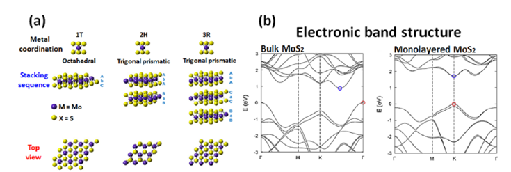
Fig. 2(a) The metal coordination in 1T, 2H, and 3R phases of MX2 (M: Mo, W; X: S, Se). (b) The electronic band structure of MoS2 (bulk), and MoS2 (monolayer). Figure adapted from references.[9-10]
A single-layer MX2 may have a trigonal prismatic (2H) or octahedral (1T) metal coordinating phase. In multiple structures, each individual layer can possess any of the two coordinating phases. Different polymorphic structures, with a large variety of different properties, can be represented by the same MX2. The most common polymorphs of MX2 are 1T, 2H and 3R, Fig. 2. The number indicates the number of layers in the crystallographic unit cell, and the letter indicates the type of symmetry. T stands for tetragonal (D3d group), H for hexagonal (D3h groups), and R for rhombohedral (C3v 5 group).[9] Fig. 2 recaps the crystalline structure of MX2 and the band structure of 2H, 1T.
The thermodynamically more stable 2H phase is most commonly found in the massive (bulk) material MX2, Fig. 2(b). The first-row of transition metals usually form the 2H coordinating phase, which is the most stable. The phase transition from 2H to 1T in MoS2 is possible through the donation of electrons, which produce a change in the XPS peak of Mo 3d to reduce the binding energy, by means of alkali-intercalation.[11] This phase transition is very important because the electronic properties of the materials are modified: 2H-MX2 is semiconductor, whereas 1T-MX2 behaves as a metal-like material. Therefore, the structural-characterization of MX2 materials is of paramount importance to take into account for the evaluation of the electrocatalytic properties. Among all MX2 materials, molybdenum disulfide, MoS2, is the first TMD to emerge as an attractive catalyst for hydrogen evolution reaction, and the material is still explored as a prototype model to better understand the behavior of nano-structured MX2-based materials.
Results and Discussion
The MoS2 properties
In general, a single-layer of MoS2 has a laminar S-Mo-S structure with a thickness of approximately 0.7 nm.[12] Each 2D layer of MoS2 consists of a hexagonal plane of Mo atoms and two S atoms of hexagonal planes modulated by the covalent interactions in trigonal prismatic form. The Mo-S length, the crystal lattice constant, and the distance between the upper and lower sulfur atoms are 2.4 Å, 3.2 Å, and 3.1 Å, respectively. [13] The absence of the (002), (103) and (105) Bragg peaks in the X-ray diffraction pattern is characteristic of one-molecule-sheet thickness.[11-13] The two main types of MoS2 semiconductor coordination phases are 2H and 3R. Phase 2H is the most thermodynamically stable. In the 1T metallic phase, Mo atoms are octahedrally coordinated, possessing a higher electrical conductivity, anisotropy, chemical stability in acid environments, and high photo-corrosion resistance.[14] These properties of MoS2 are due to the anti-bonding state as a result of the interaction between Mo dz 2 orbitals and S p z orbitals at the top of the valence band.[15] Since the band-gap energy varies with the number of layers, [8,16] the band-structure is a property that can be tuned. As the thickness of MoS2 decreases to the size of a monolayer, cf. Fig. 2, a transformation from the indirect band-gap (1.3 eV) to the direct band-gap (1.9 eV) is observed.[8] Based on computational approach using the density functional theory (DFT), the suggested explanation for this band-gap transition was that the top-edge of the valence band and the bottom-edge of the conduction band, on MoS2, are located at the Γ point, almost halfway along Γ-Κ direction, respectively, [10] Fig. 2(b). With the increasing number of layers, the bottom-edge of the conduction band moves upward, increasing the overall band-gap. The conduction band states at the Κ point are mainly associated with Mo d-orbitals and are relatively unaffected by the interlayer interaction. The direct band-gap at the Κ point only increases approximately 0.05 eV to 0.1 eV. [16] The states near the Γ point on the conduction band, due to the hybridization between S p z -orbitals and Mo d-orbitals, are strongly dependent on the interlayer interaction. Hence, the bands at the Γ point are remarkably affected by the decrease in the number of layers. Therefore, for a mono-layer structure, the indirect transition gap is larger than the direct transition gap. The direct band-gap (ca. 1.9 eV) at the Κ point becomes the smallest gap.[16]
Water splitting
The water splitting is a chemical reaction (eq. 1) in which water is separated into hydrogen and oxygen.[17] Regardless of the electrolyte, at standard conditions (1 bar and 298 K), the reaction requires a minimum energy, ΔG = 237.1 kJ mol-1, or ΔE = 1.23 V. Higher potentials (overpotential) applied to the electrodes are required to activate the intrinsic kinetic barriers present in the anode and the cathode materials. This matter is still open, since efforts are being done nowadays to tailor highly active novel materials, based on non-precious catalytic centers, to reduce the overpotential.[18]
In addition to water splitting via electrolysis, the reaction can also be performed by photocatalysis.[19] The conduction band energy and valence band energy levels rely on the band-gap and the position in the electrochemical energy scale of a semiconducting material to straddle the redox potential of water, E° H + /H2 , E° O2/H2O , and to absorb the visible-region spectrum photons to generate efficiently e-/h+ pairs. Moreover, an efficient cost-effective artificial photosynthesis for water splitting needs to be further developed.[20] The current status of this approach has been discussed recently.[21]
Hydrogen evolution reaction electrocatalysis
The protons (acid environment) or water molecules (alkaline environment) are reduced in a half-cell reaction to evolve to gaseous hydrogen. In acid conditions, the overall hydrogen evolution reaction (HER) is represented by eq. (2).
The activation energy of this reaction, reflected by the magnitude of the overpotential, (, is needed to overcome the energy barrier. The role of the electrocatalytic material is to decrease the activation energy, and/or the magnitude of the overpotential. In acid medium, the HER is well-established to proceed in various steps, that is:
Volmer step:
Heyrovsky step
Tafel step:
where, * denotes the surface-active site of the electrode.
In the classical view, the Tafel slope can suggest the reaction determining step (RDS). Tafel slopes of 120, 40 and 30 mV dec-1 are associated to Volmer, Heyrovsky and Tafel RDS, respectively. The HER can be either due to the Volmer-Heyrovsky, or Volmer-Tafel mechanisms. For the HER the Volmer step is the initial event involving the adsorption of hydrogen atom (M-Hads) at the surface of the electrode (M). Thus, the descriptor of the reaction is the free energy of hydrogen adsorption, ΔG H + . According to the Sabatier’s principle, if ΔG H + is too weak, the adsorption step will limit the overall reaction rate. Moreover, if ΔG H + is too strong, the desorption step will limit the overall reaction rate. That is why an optimal HER catalyst has values of ΔG H + close to zero. This principle gives rise to the construction of a volcano curve, Fig. 3. This figure summarizes the HER exchange current density, j 0 , of catalytic metal centers, as function of ΔG H + .

Fig. 3 The exchange current density, j 0 , as a function of the hydrogen-adsorption free energy, ΔG H + , for selected hydrogen Evolution Reaction-metal centers. Data are displayed in a Volcano type-plot. The activity of MoS2 is also displayed. Data adapted from ref. [1].
The ideal electrocatalyst possesses properties such as high surface area, high active-sites density, high electrical conductivity, high chemical stability, optimal adsorption properties, and facile (scale-up) way of synthesis. Therefore, to optimize the HER kinetics, tailoring and tuning the properties of a catalyst is of paramount importance. In this regard, the HER mechanism on different surfaces was studied employing the DFT calculations by Hinnemann et al. [22] These authors revealed that nanostructured MoS2 possesses a ΔG H + value close to zero, cf. Fig. 3, thus, the proton adsorption energy was comparable to that of Pt.[22] This fact indicated that MoS2 is a potential HER electrocatalyst, as demonstrated experimentally by Jaramillo et al.[23] The sulfur-edge sites of nanostructured MoS2 were identified as the real active electrocatalytic HER sites. Therefore, nanostructured MoS2, possessing a high density of sulfur-edges sites, is considered as a highly active material for the HER. Moreover, the design and fabrication of MoS2-based materials, with a significant activity and stability towards the HER still remain a challenge. Consequently, several strategies such as the use of nanoparticles and nano-sheets by defect-surface engineering,[24] MoSx amorphous-like films14 the hybridization with some transition-metal, e.g., Ni[25] or Co[26] have been considered. Moreover, a very useful strategy (phase transition 2H to 1T), which consists in intercalating Li-ions in MoS2 to obtain 1T MoS2 nano-particles and/or nano-sheets, has been widely used.[24-27] For example, Lukowski et al.[27] prepared 1T-MoS2 nano-sheets grown onto graphite via a chemical vapor deposition method. They observed that the HER kinetics dramatically enhanced, reporting a Tafel slope of 43 mV dec-1, and a cathodic overpotential of 187 mV at 10 mA cm-2. The authors attributed the HER enhancement to the metallic-like behavior, and a high density of defects generated on 1T-MoS2 structure.[27] In spite of this phenomenon, 1T-MoS2 nano-sheets showed a poor stability,[14] due to the reconversion of 1T to 2H semiconducting phase, a phenomenon that occurs even at moderated-annealing-temperature of 95°C.
On the other hand, the electrochemical impedance spectroscopy (EIS) analysis of MoSX films, electrodeposited onto glassy carbon disks, suggested an electronic coupling between the amorphous molybdenum sulphide and the conductive carbon material, as claimed by Vrubel et al.[28] Such coupling was important to enhance the kinetics towards HER. Since the low conductivity of MoS2 is a problem,1 chemically-exfoliated MoS2 nano-sheets with a high concentration of metallic 1T phase and the presence of semiconducting 2H phase was reported by Voiry et al.[29] Both phases were integrated with carbon nanotubes and were evaluated towards the HER in 0.5M H2SO4. These structures showed a high performance towards HER, with a Tafel slope of 40 mV dec-1, assessing the importance of the electrical conductivity enhancement. Therefore, the integration of MoS2-nanostructures with conductive support-materials is an effective way to activate the catalytic centers. These nanostructures justify the fact of mediating the growth, dispersing catalytic nanoparticles, and providing electrons for the electrocatalytic activation. Taking advantage of the properties of reduced graphene oxide, RGO, Li et al.,[30] prepared hybrid materials: MoS2/RGO. Their results revealed that the integration of RGO with MoS2 also enhanced significantly the HER kinetics in acid, due to a rich active edge site of the small particle size, and the “synergy effect”, i.e., the interaction effect arising between MoS2 and RGO (acting as support). However, the “synergy effect” between MoS2 and carbon support-materials was not further discussed. Although the limited electrical conductivity of MoS2 has been circumvented by coupling the TMD with carbon support materials, there are not enough studies discussing the interaction of the catalytic center with the support. Some hints are, moreover, provided by Niu et al.[31] The synchrotron X-Ray Absorption Spectroscopy (XAS) was used to study the synergy effect between nanoplates of MoS2, with a high density of unsaturated sulphur-edges and a short distance between basal planes to edges, on carbon nanofiber, CNF, see inset in Fig. 4(a). The CNF in the system MoS2/CNF receives more electrons in the high-energy (* states than in the low-energy π* states, resulting in a more weighted unoccupied π* states. In addition, as further revealed by the XANES spectra of Mo-L2 edge, and S K-edge, Figures 4(a) and (b), the wider peak of Mo-L2-edge suggests electron transfer of Mo 4d to C 2p states, as a result of the interaction of the TMD with the support, whereas on the S K-edge, besides the signal of the TMD (peak A) the enhanced peak B put in evidence the reactivity of S at the edges with oxygen. Summing up, the interaction phenomenon increases the graphitic character of CNF in the MoS2/CNF system, favoring the conduction of electrons and thus the HER kinetics, Fig. 4(d). On the other hand, photocatalysis is also favored on the same system due to the electronic interaction between MoS2 and CNF via the presence of a photosensitizer (FL: fluorescein), Fig. 4(c). These results contrast that, by inducing a strong MoS2-carbon interaction, the overall HER performance is increased.

Fig. 4 For the system MoS2-CNF: (a) Mo-L2 edge XANES spectra. (b) S-K edge XANES spectra. (c) photo-electrocatalytic HER on MoS2-CNF, photosensitized by the presence of fluorescein (FL). (d) The electrocatalytic HER on CNF, MoS2, Pt and MoS2-CNF materials. Data adapted from ref. [31]
In order to compare the performance of MoS2-based catalysts, the Tafel slope and the overpotential to drive -10 mA cm-2, Ƞ@10, are considered. The Ƞ@10 is the electrode-activity parameter considered as an optimal metric for solar fuel applications.[1] The Tafel slope determines the additional potential required to increase the kinetic current by an order of magnitude. Thus, low Tafel slope values are desirable (as close as possible to 30 mV dec-1), specifically for high-current applications, e.g., in electrolyzer devices. Fig. 5 summarizes HER activity state-of-the-art collected data so far on MoS2 electrocatalysts in acid medium. We can clearly appreciate the positive evolution of MoS2-based catalysts based on the materials’ engineering between the catalytic center and the support. This approach influences the HER mechanism. As discussed in the literature, the defect engineering and change of the phase transition to 1T coordination assure a robust surface defect-density, identified as the real active sites for HER. Unfortunately, the stability of such nano-structures, as well as their electrical conductivity are still to be improved. This is the reason, to this day, that the coupling with conductive carbon supports of MoS2-structures offer the highest HER performance. To our best knowledge, the strong interaction between the catalytic center and the support can improve the activity and stability of the catalytic center. An approach that has to be considered in the majority of nanoparticulated electrocatalytic centers to enhance reactions of technological importance.

Photocatalysis of the hydrogen evolution reaction
A reference material which is widely used for the photoelectrocatalytic hydrogen production is the TiO2 (anatase phase) decorated with a metal co-catalyst, e.g., Pt. The performance determined by the optical limit under AM1.5 Global irradiation of oxides (e.g., TiO2, Fe2O3, WO3) is extremely low for the overall water splitting.[32] Moreover, a constant effort has demonstrated that chalcogenides (MoS2-based) are attractive materials for water splitting photoelectrocatalysis. The p-type conductivity of MoS2 films (Eg = 1.87 eV) has been reported by Liu et al.[33] Therefore, p-n heterojunctions based p-MoS2 and n-CdS (Eg = 2.4 eV), Fig. 6(a), were efficient and stable for the HER under visible irradiation.[16] The photogenerated electrons (e-) at the conduction band (CB) of MoS2 are conveyed to the counter electrode (where HER proceeds) via the CdS CB, whereas the photogenerated holes (h+) at the CdS valence band (VB) are transferred to the MoS2 VB avoiding the photo-corrosion of CdS.
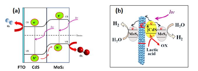
Fig. 6(a) p-n MoS2/CdS heterojunction for the water splitting under visible irradiation. Adapted from ref. [33]; (b) Photocatalytic hydrogen evolution under visible light, and a sacrificing agent - hole scavenger (Lactic acid). Adapted from ref. [35]
A similar heterojunction produced by electrospinning mediated photo-deposition technique using oxide nanofibers (TiO2-NF) was developed by Qin et al.[34] The resulting system schematized in Fig. 6(b) is MoS2/CdS-TiO2-NF. Alike the system shown in Fig. 6(a), the MoS2/CdS-TiO2-NF system was designed for the visible-light photocatalytic hydrogen production. A sacrificing agent (lactic acid) serving as hole scavenger was used. Under this condition, the H2 evolution was 3 - 4 times higher on MoS2/CdS-TiO2-NF than on MoS2/CdS-P25 and Pt/CdS-TiO2.
Taking advantage of the unique electrical properties of 1D and 2D carbon nano-structures, [35] nanostructures based on the TMD and carbon, photocatalysts were designed for the photocatalytic hydrogen evolution. As shown in Fig. 4, nanohybrids by nanoplates deposition of MoS2 nano-structures onto carbon nanofibers and a photosensitizer (FL) were evaluated toward the photocatalytic hydrogen production by Niu et al.[31] The HER rate increased considerably as a result of the synergy effects of the semiconductor with the carbon support. Moreover, a high HER photo-activity was observed on MoS2/graphene as co-catalyst on TiO2 nano-crystals.[15] The presence of graphene network in this system facilitated the charge separation generated at the semiconducting materials thus avoiding, the charge recombination, and increasing the hydrogen production rate by a factor of 39, i.e., 4 times higher than the rate on TiO2, and on TiO2-MoS2. The consensus on carbon (graphene) on MoS2-carbon, as HER photo-catalysts, as activity enhancer is due to the extended charge separation, less charge recombination on this graphene network, as assessed on various reports.[2,16,35]. This is certainly an avenue, and the reason why future works should address the interaction between the catalytic center, e.g., MoS2 and the support.
Conclusion
Layered-based nanostructured TMD are promising materials for electrocatalysis of HER and photocatalysis for water splitting technology. Understanding the properties of such nano-structures is extremely important to tailor and tune their performance towards electrocatalytic processes. A widely studied example is the limited electrical conductivity of molybdenum disulfide. Although many authors claim that the coupling between carbon surfaces and MoS2 catalytic-centers enhances the HER kinetics, there are very few studies which discuss deeply this important “ingredient” to tune a high active and stable HER catalyst. To the best of our knowledge, the strong interaction between the catalytic center and its support can improve the activity and stability of a given photoelectrocatalytic material. Therefore, inducing a strong MoS2-carbon interaction is proposed to be a novel strategy in the MoS2 performance towards HER.

