


Serviços Personalizados
Journal
Artigo
 Espanhol (pdf)
 Artigo em XML
 Referências do artigo
 Enviar este artigo por email
Indicadores
-
 Citado por SciELO
 -
 Acessos
Links relacionados
-
 Similares em
SciELO
Similares em
SciELO
Compartilhar

 Permalink
Ingeniería mecánica, tecnología y desarrollo
versão impressa ISSN 1665-7381
Ingenier. mecáni. tecnolog. desarroll vol.4 no.3 México Set. 2012
Artículos
Silver nano-particles sintering process for the die-attach of power devices for high temperature applications
L.A. Navarro, X. Perpiñà, M. Vellvehi, X. Jordà
Institut de Microelectrónica de Barcelona-Centre Nacional de Microelectrónica (IMB-CNM), Campus UAB Bellaterra, 08193, Cerdanyola de Vallès (Barcelona, Spain) Teléfono: +34 935947700 luis.navarro@imb-cnm.csic.es, xavier.perpinya@imb-cnm.csic.es, miquel.vellvehi@imb-cnm.csic.es, xavier.jorda@imb-cnm.csic.es.
Fecha de recepción: 08-06-2012
Fecha de aceptación: 21-08-2012
Resumen
La capa de die-attach (unión entre un dispositivo semiconductor y su substrato), es uno de los elementos más críticos de la electrónica de potencia, sobretodo en aplicaciones de alta temperatura. Debido al aumento de la temperatura de operación son necesarios nuevos materiales, con puntos de fusión más altos y propiedades termo-mecánicas adecuadas. Dentro de las posibles soluciones (tecnológicas y nuevos materiales), la sinterización de nano-partículas de Ag, es una solución interesante, ya que sólo requiere una moderada temperatura de proceso (<300 °C). El objetivo de nuestro trabajo es la implementación y evaluación experimental de la técnica de sinterización de nano-partículas de Ag para el die-attach sobre substratos de Cu. La calidad del die-attach se evaluará en vehículos de prueba mediante ensayos de die-shear. En este trabajo presentaremos, el método de procesado, análisis de algunos parámetros que influyen en el proceso y los principales resultados obtenidos tras los procesos de sinterización de nano-Ag.
Palabras clave: nano-sinterizado de plata, die-attach, encapsulado, dispositivos de potencia.
Abstract
Die-attach layer is one of the most critical elements for high-temperature power electronics applications. The increase in operating temperature requires new materials with higher melting points and suitable thermo-mechanical properties. Among the possible solutions, sintering of Ag nano-scale particles is an interesting method, because it requires moderate (<300°C) process temperatures. The aim of this work is the implementation and experimental evaluation of nano-Ag sintering for the die-attach of semiconductor power devices, directly on Cu substrates. The experimental evaluation of the die-attach integrity will be performed using test vehicles and die-shear analysis tools. In this paper, processing methodology, analysis of some parameters that influence the process and die-shear results of nano-Ag sintered samples, will be presented.
Keywords: silver nano-sintering, die-attach, packaging, power devices
Nomenclature
Li Initial sintered layer length
Ls Sintered layer length after densification
Lf Final sintered layer length
m Constant dependent of sintering type
p Porosity
Ra Arithmetic surface roughness (nm)
r Particle radius (nm)
t Sintering time (min)
Vv Volume of the voids in the layer (nm)
Vf Volume of the final layer (nm)
Introduction
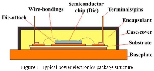
Today, there is an increasing interest for high-temperature power electronics systems, mainly driven by the development of wide band-gap semiconductor devices (SiC, GaN). Space and harsh environment electronics are two of the main application areas. However, determining the appropriate packaging technology for these application niches is an open topic. Therefore, significant research efforts are currently addressed [1, 2, 3, 4]. In this framework, the semiconductor to substrate joint (die-attach) is one of the most challenging power packaging elements (Figure 1): as the mechanical properties of die-attach materials decrease on harsh environments, a safety margin should be kept between the operating temperature and the melting point of the die-attach material. This margin is defined by the so called homologous temperature, the ratio between the operating and the die-attach melting temperatures expressed in Kelvins. For high temperature power electronic applications, it ranges from 0.8 to higher values [5]. However, even with such a high value, it can be seen that as the operating temperatures increase, soldering alloys with much higher melting points are required, i.e., for an operating temperature of 200°C (473 K), a melting point of 318°C (473/0.8 = 591 K) is necessary. This requires a high temperature bonding process, resulting in an increased level of residual stresses.
At this moment, several efforts are invested in determining which materials and techniques are the most suitable for high temperature die-attach. Among the candidates, we can mention solder alloys (such as AuSn, PbSnAg, AuGe, AuSi), nano- and micro-particle sintering (typically with Ag) and transient liquid phase bonding [6, 7, 8]. The two last solutions are the most attractive because the bonding process can be performed at a temperature lower than that of the die-attach melting point. Besides, they present the advantage of a low level of residual stress (low-temperature process) and high melting temperature (wide safety margin between operating temperature and melting point).
This paper focuses on the sintering technology. We present the developed processing methodology for nano-Ag sintering of semiconductor dies on Cu substrates, analyzing some critical process parameters (substrate roughness and sintering pressure). It is worth to point out, that although many data is available about nano-Ag sintering on Ag and Au surfaces, few results have been reported up to date about sintering over Cu substrates. Finally, we discussed the main experimental characterization results obtained from different test vehicles.
Nano-Ag sintering process description
Generally, sintering die-attach solutions use silver as the base material, since it offers excellent properties for die-attach. Among these properties one can highlight its high melting temperature (961°C), high thermal conductivity (430 W/m.K) and high electrical conductivity (0.63 x 10⁶ Ω-1cm-1). The Ag powder is dispersed in organic components to allow its dispensing as a paste. The pastes differ by the size and shape of the silver particles, as well as by their organic components (dispersant, binder, and thinner). Dispersant, binder, and thinner are added to Ag powder respectively, to produce a paste with good particle dispersion, flowability and adequately viscosity for screen printing [9, 10, 11]. The selection of the right organic components is critical in order to avoid the formation of aggregates and agglomerates in the paste. Aggregates are clusters of interconnected nano-parti-cles strongly bonded together by solid necks. In a powder with aggregates, the effective particle size is higher than that of the individual particles, and the benefits of using nano-scaled powder are reduced.
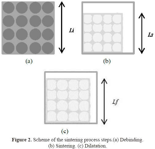
The sintering process produces bulk materials by heating and pressing some powder under its melting temperature. Figure 2 depicts a sintering process and highlights its different phases. They are [11]:
1. Debinding consists in the volatilization of the organic components which coat the particles to sinter. Debin-ding is an essential step which prevents the formation of voids in the bulk material. Figure 2a shows the initial size (Li) of the nano-Ag paste layer before sintering, which is not significantly modified during debinding.
2. Sintering is the step of densification where particles are getting bigger and the number of internal voids decreases. The scheme of Figure 2b depicts the associated dimensions reduction, where the initial size of the Ag paste layer (Li) decreases up to a smaller intermediate sintering size Ls.
3. Dilatation (Figure 2c) can occur after densification in case of recrystallisation, in particular for metallic materials.
The main experimental parameters having an influence on the kinetics of the sintering process are:
1. Temperature profile: The temperature profile can be divided in two parts: a first progressive temperature increase to assist the debinding phase and a final high temperature step during the sintering phase (sintering time). Sintering time decreases when sintering temperature increases.
2. Sintering pressure: When the pressure applied during the sintering increases, the sintering temperature can be reduced.
3. Particle size: The sintering time (t) depends on the particles radius (r), as dictates Herring's law:
where r1 and r2 are the initial and final radius of the particles during sintering at times t1 and t2 respectively and m is a constant which depends on the type of sintering (between 4 and 8) [3].
From equation (1), it can be inferred that smaller particles sinter much faster, with drastical reductions of the sintering times for r < 50 nm. In addition the nano-size is adequate for low temperature (T < 300°C) and low sintering pressure (a few Mpa). For example, powders based on micron-scale particles require pressures up to 40 Mpa [12, 13]. For such pressure values, specific tooling is necessary for avoiding the die fracture. In special conditions, sintering at room temperature becomes possible [14].
One of the parameters determining the quality of the sintered layer is its porosity (P), which is defined as:
where Vv and VT are the voids and final sintered layer volumes, respectively. This parameter has a significant impact on thermal and electrical conductivities of the sintered layer. Porosities between 15% and 30 % are reported in the literature for good quality nano-Ag sintered layers [15, 16].
Another figure of merit used for characterizing the sintered layer quality is the die-shear force required for removing the chip from the substrate. This parameter allows quantifying the adherence provided by the die-attach, and it can be expressed either as a force or as a stress (dividing the force by the die area). Die shear values between 20 MPa and 30 MPa are reported in the literature for chips with areas higher than than 4 mm2.
Test vehicle used for nano-Ag sintering experiments
The evaluation of the nano-Ag sintering technology has been conducted on test vehicles depicted in Figure 3. Figure 3a shows the basic cross section of the test vehicle with its main parts: die, die-attach layer and substrate. Figure 3b provides a top view showing the 6 Silicon dies assembled to the substrate. The benefit of considering multiple dies in each sample is that allows obtaining a significant statistical distribution of die adhesion to the substrate, being possible to extract information about the developed sintering process.
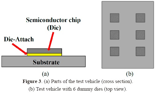
For preparing the test vehicle, silicon dummy dies have been chosen instead of functional devices as this work aims at studying mainly the mechanical adhesion provided by the Ag sintered layer. This approach constitutes a good base for subsequent studies using other semiconductors such as SiC which are more expensive than Si. The used dies are 300 [im thick, with a 2.8 x 2.8 mm2 area. These dimensions are representative of real power devices [17]. The backside metallization includes four metal layers of different thickness: Al (0.5 µm) / Ti (100 nm) / Ni (500 nm) / Au (200 nm).
The aiming of this multiple layer metallization is to allow a good ohmic contact with the semiconductor (Al), to ensure a good adherence (Ti), to establish a diffusion barrier (Ni) and to avoid surface oxidation (Au). The roughness of the chips backside was 30 nm.
Concerning the substrate, Copper has been used because it provides high thermal conductivity, easy machinability and lower cost than ceramic substrates. Many results about nano-Ag sintering on Ag and Au plated substrates are described in the literature, but few information is available for Cu. Besides, the Cu coefficient of thermal expansion (17 ppm/°C) is higher than that of other used metal baseplates such as Kovar (6 ppm/°C). Therefore, our test vehicle can be considered the worst case scenario. The dimensions of the Cu substrate are 15 mm x 20 mm x 0.8 mm, which are similar to those of the TO-247 package.
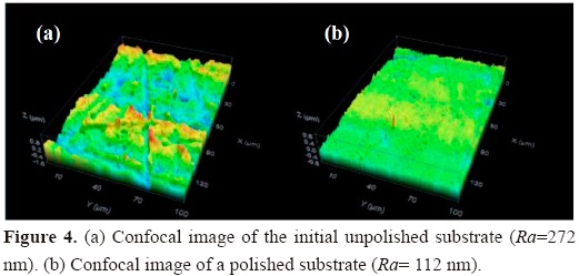
An important parameter influencing the adhesion of the sintered Ag layer is the substrate roughness (Ra). The initial Cu substrates used in this work, show Ra values around 272 nm. This mean value was obtained using confocal microscope measurements on five small areas (138 x 102µm2) of the substrate surface. In order to analyze the effect of different Ra values, we used two types of polishing slurry. The polished substrates have shown mean Ra values around 112 nm and 28 nm respectively. The confocal images of Figure 4 evidence the difference between an unpolished and a polished substrate.
For the die-attach, we have used a nanoTach-K Ag paste from NBE Tech [18].
Nano-Ag sintering procedure and evaluation
Before sintering, the Cu substrates and the Si dies require an accurate cleaning and conditioning process. This process starts with acetone (10 minutes in ultrasonic bath) to remove the organic contaminants, for the Cu substrates it continues with a deoxidization using an etching product and a final isopropanol cleaning to remove any remaining impurity (10 minutes in ultrasonic bath).
The nano-Ag paste is deposited on the Cu substrate by screen printing. The corresponding mask is 100 µm thick and it allows placing a controlled volume of paste for each chip of the test vehicle. Then, the dies are placed on the fresh nano-Ag paste and at this point the thickness of the die-attach is set to 60 [im.
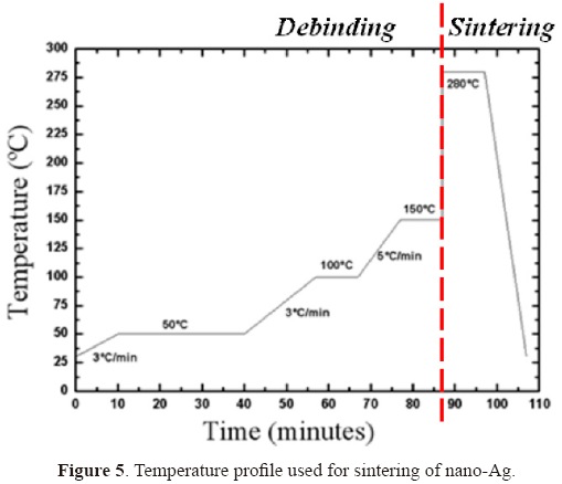
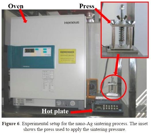
The temperature profile starts with the debinding phase, which is made of three successive steps at 50°C, 100°C and 150°C (Figure 5), where the organic components vaporize. Then, the temperature is quickly increased up to 280°C and the sintering process takes place. The debinding is realized in an oven in air ambient, whereas the sintering step is performed on a hot plate with the test vehicle placed on a specifically designed press (Figure 6). This press applies a constant uniaxial pressure controlled by a stainless steel spring, which is suitable for 300°C operation. After sintering, the system cools down naturally, so the overall cycle time takes around 2 hours.
The final thickness of the sintered Ag layer at this point ranges between 20 µm and 35 µm depending on the applied pressure. This means a densification factor between 30 % and 60 %.
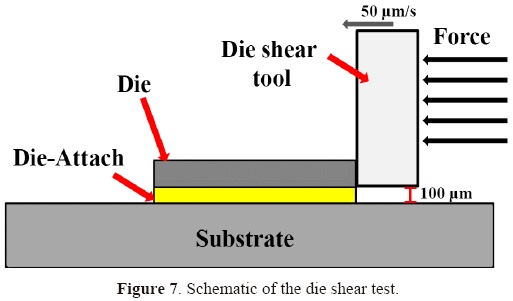
Finally, mechanical adhesion is evaluated in each test vehicle using die shear tests [19]. In our case the die shear test was performed using a Royce 650 system. The die shear tool height was set at 100 µm above the substrate and the die shear speed was 50 µm/s (Figure 7). Although the main objective of the die shear tests is to evaluate the quality of the joint, it allows also evaluating the reproducibility of the process. The process is considered reproducible if there is a small dispersion of the die shear force required to remove the dies in subsequent experiments.
In order to determine the optimum sintering process parameters, nine different series of test vehicles were fabricated and evaluated following the explained procedures (Table 1).
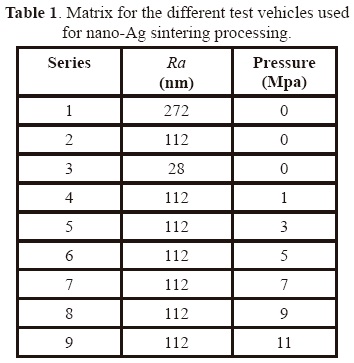
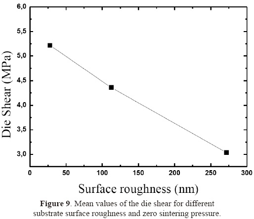
The Series 1, 2 and 3 correspond to Cu substrates showing different surface roughness and were realized without sintering pressure applied to the dies. Three different values of roughness were used (272 nm, 112 nm and 28 nm).
The Series 4 to 9 were realized with the same roughness of the Cu substrate (112 nm) but different sintering pressure levels from 1 MPa up to 11 MPa. Figure 8 summarizes the test matrix results, showing the main statistical parameters in the box-diagram plot. It can be observed that the best results (higher die-shear strength) are obtained with an applied pressure during the sintering process, the zero pressure series give too low shear values (below 5 MPa) and that the increasing pressure gives higher die-shear values. It can be also observed that the proposed sintering process is associated with a relatively high dispersion.
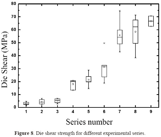
Figure 9 shows more specifically the influence of the substrate surface roughness on the mean value of the shear strength for Series 1-3 (zero pressure). As it can be observed, the die shear increases with low values of roughness.
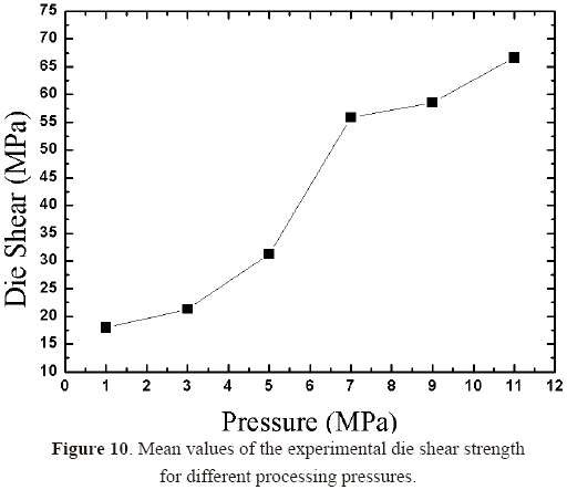
On the other hand, Figure 10 shows the sintering pressure influence, where the mean die-shear strength increases when increasing the processing pressure.
Conclusions
We present an Ag nano-particle sintering process methodology for die-attach applications, evaluated on different test vehicles. The test vehicles include six Si dies, the die-attach layer and a Cu substrate. The influence of different processing parameters (substrate surface roughness and applied sintering pressure) has been evaluated. It has been shown that when the substrate surface roughness decreases, the die-shear strength increases. On the other hand, when the sintering pressure increases, the die-shear strength also increases. The obtained results comply with the acceptance criteria of the MIL-STD-883H standard concerning die-attach evaluation [19].
Finally, we concluded that it is necessary to study the coupled influence of the substrate roughness and sintering pressure together. For this reason at this moment, we are undertaking several experiments with different values of roughness and sintering pressures simultaneously. Thermal cycling experiments will also be performed on similar test vehicles.
Acknowledgements
This work is partially funded by the Spanish Ministry of Economy and Competitiveness through the Research Program RAMON Y CAJAL (contract no: RyC-2010-07434), the THERMOS Project (contract no: TEC2008-05577 -FEDER), the CONSOLIDER-RUE Project and TRENCH-SIC Project (contract no: TEC2011-22607).
References
[1] P. Zheng, P. Henson, R. W. Johnson. "Pack-aging Technology for Electronics Applications in Harsh, High-Temperature Environments". IEEE Transactions on Industrial Electronics, Vol. 58, No. 7, pp. 2673-2682, 2011. [ Links ]
[2] R. W. Johnson, C. Wang, Y. Liu, J. D. Sco-field. "Power Device Packaging Technologies for Extreme Environments". IEEE Transactions On Electronics Packaging Manufacturing, Vol. 30, No. 3, pp. 182-193, 2007. [ Links ]
[3] A. Masson, C. Buttay, H. Morel, C. Raynaud, S. Hascoet and L. Gremillard."High-Temperature Die-Attaches for SiC Power Devices". Proceedings of the 14th European Conference on Power Electronics and Applications (EPE'2011), pp. 1-10, 2011. [ Links ]
[4] L. Coppola, D. Huff, F. Wang, R. Burgos, and D. Boroyevich. "Survey on High-Temperature Packaging Materials for SiC-Based Power Electronics Modules". Proceedings of the IEEE Power Electronics Specialist Conference (PESC'2007), pp. 2234-2240, 2007. [ Links ]
[5] C. Buttay, A. Masson, J. Li, M. Johnson, M. Lazar, C. Raynaud. "Die Attach of Power Devices Using Silver Sintering Bonding Process Optimisation and Characterization". Proceedings of the High Temperature Electronics Network (HiTEN), 2011. [ Links ]
[6] V. R. Manikam and Kuan Yew Cheong. "Die Attach Materials for High Temperature Applica-tions: A Review". Proceedings of the IEEE, Vol. 1, Issue: 4, pp. 457-478, 2011. [ Links ]
[7] R. Kisiel, Z. Szczepanski. "Die-attachment solutions for SiC power devices". Microelectron-ics Reliability, Vol. 49, pp. 627-629, 2009. [ Links ]
[8] H.A. Mustain, W.D. Brown, S.S. Ang. "Transient Liquid Phase Die Attach for High-Temperature Silicon Carbide Power Devices". IEEE Transactions On Components and Packag-ing Technologies, Vol. 33, No. 3, pp. 563-570, 2010. [ Links ]
[9] J. G. Bai, Z. Z. Zhang, J. N. Calata and G-Q. Lu. "Low-Temperature Sintered Nanoscale Sil-ver as a Novel Semiconductor Device-Metallized Substrate Interconnect Material". IEEE Transac-tions On Components and Packaging Technologies, Vol. 29, No. 3, pp. 589-593, 2006. [ Links ]
[10] G. Bai. "Low-Temperature Sintering of Nanoscale Silver Paste for Semiconductor De vice Interconnection". PhD thesis, Virginia Poly-technic Institute and State University. Blacks-burg, Virginia, October 2005. [ Links ]
[11] G-Q. Lu, J. N. Calata, and T. G. Lei. "Low-Temperature Sintering of Nanoscale Silver Paste for Power Chip Attachment". Proceedings of the International Conference on Integrated Power Systems, pp. 1-5, 2008. [ Links ]
[12] H. Schwarzbauer and R. Kuhnert, "Novel large area joining technique for improved power device performance". IEEE Transactions on Industry Applications, Vol. 27, pp. 93 -95, 1991. [ Links ]
[13] C. Göbl, J. Faltenbacher. "Low temperature sinter technology Die attachment for power elec-tronics applications". Proceedings of the Interna-tional Conference on Integrated Power Electron-ics Systems, pp. 1-5, 2010. [ Links ]
[14] D. Wakuda, K.-S. Kim, and K. Suganuma. "Ag Nanopar-ticle Paste Synthesis for Room Temperature Bonding". IEEE Transaction on Components and Packaging Technology, Vol. 33, pp. 1-6, 2010. [ Links ]
[15] T. G. Lei, J. N. Calata, G-Q Lu, X. Chen and S. Luo. "Low-Temperature Sintering of Nanoscale Silver Paste for Attaching Large-Area (>100mm2) Chips". IEEE Transactions On Components and Packaging Technology, Vol. 33, No. 1, pp. 98 -104, 2010. [ Links ]
[16] J. Kahler, N. Heuck, A. Stranz, A. Waag, and E. Peiner. "Pick-and-Place Silver Sintering Die Attach of Small-Area Chips". IEEE Transac-tions On Components Packaging and Manufac-turing Technology, Vol. 2, No. 2, pp.199-207. February 2012 [ Links ]
[17] P. Godignon, X. Jordà, M. Vellvehi, X. Perpiñá, V Banu,D. López, J. Barbero, P. Brosselard, and S. Massetti. "SiC Schottky Di-odes for Harsh Environment Space Applications" IEEE Transactions on Industrial Electronics, Vol. 58, No. 7, pp. 2582-2589. July 2011. [ Links ]
[19] MIL-STD-883H

