


 nueva página del texto (beta)
 Inglés (pdf)
 Artículo en XML
 Referencias del artículo
 Enviar artículo por email
 Citado por SciELO
  Similares en
SciELO
Similares en
SciELO 
 Permalink
1. Introduction
To generate bulk amount of AC electrical energy, fossil fuels have been used for centuries. But, the use of fossil fuels such as coal, natural gas, and petroleum, leads to serious environmental contaminations, public health issues, and increased cost of the power generation systems. Moreover, the existing fossil fuels are fast depleting and non-renewable. Due to the above drawbacks of conventional non-renewable energy systems, the researchers concentrated on an alternate scheme called the renewable form of power generation systems. One of the renewable energy sources like photovoltaic (PV) modules can be used to generate electrical energy in the form of DC. However, the DC output voltage from the PV source is low, and fluctuating due to the changes in sun irradiation and temperature. The low level DC output voltage of the PV source can be converted into a high level DC output voltage using an intermediate high gain DC-DC power electronic converter. This high level DC output voltage is to be fed to a grid connected inverter for producing AC electrical power. Hence, an appropriate high voltage gain DC-DC conversion stage needs to be developed with significant features of reduced voltage-current stress for the power switches and low ripples in the input current.
High voltage gain DC-DC converters can be divided into isolated and non-isolated topologies (Behera et al., 2020; Chen et al., 2019; Dobi & Sahid, 2020; Forouzesh et al., 2018; Girija & Murali, 2021; He & Khaligh, 2017; Mumtaz et al., 2021; Murali, 2021; Murali & Annapurani, 2019; Murali & Annapurani, 2021; Saravanan & Ramesh Babu, 2019; Shahir et al., 2017; Shahir et al., 2019; Siddharthan & Balasubramanian, 2019; Sowmya & Murali, 2019; Wang et al., 2019). The DC input and DC output ports are isolated using a high frequency transformer in the case of isolated DC-DC converter configurations where high voltage gain proportional to the kVA rating of the transformer can be achieved. But the overall efficiency of the transformer-based converter topologies is reduced due to certain factors such as (i). voltage spikes on the power switches due to the transformer’s leakage inductance and higher amount of power dissipation, (ii). electromagnetic interference (EMI) problems. The structure and the control of the isolated configurations are also complicated. However, the simplified structure, high efficiency and the simple control of the non-isolated DC-DC converter configurations make it more desirable for electric vehicle (EV) applications (Chen et al., 2019; Wang et al., 2019).
The conventional two-level single-switch DC-DC boost converter can achieve high voltage conversion ratio at duty cycle value nearer to unity (Hsieh et al., 2013; Hua et al., 1994). But the high duty ratio results in reduced efficiency of the converter due to the increased conduction and switching losses. Another way of obtaining high voltage gain is by connecting a number of boost converters in series, which may lead to the high cost of conversion scheme.
A large voltage gain applied to fuel cell can be achieved using quadratic boost converter topologies (Leyva-Ramos et al., 2017; Wang, Qiu et al., 2019). But, these topologies have a relatively large amount of switching power losses due to high voltage stress occurring in the transistors. Some authors proposed a coupled inductor based quadratic boost DC-DC converter with high voltage gain and reduced switch voltage stresses (Lee & Do, 2019). The high voltage gain can also be achieved using multilevel converter topologies in which the transistors have lower voltage stress. However, the multilevel topologies have the disadvantage that more number of semiconductor devices needs to be used (Jiang et al., 2018).
Non-isolated non-coupled inductor based DC-DC converter topologies have also been used to achieve high voltage gain (Annapurani & Murali, 2020; Arab & Shokrollahi, 2019; Varesi et al., 2017). Due to the absence of magnetic components, the non-coupled inductor based DC-DC converter structures can produce high voltage gain with high power density and better efficiency. To improve the voltage gain of the converter, the switched-inductor (SI) and switched-capacitor (SC) based DC-DC converters with transformerless structures are also used, where the major issues are the high current and voltage stresses occurring on the power switches (Ajami et al., 2015; Jiao et al., 2011; Kim et al., 2019; Stala et al., 2019; Wu et al., 2015). Hence, the coupled inductor approach was used to achieve high voltage conversion ratio (Axelrod et al., 2015; Liu et al., 2016; Mulla et al., 2021). However, the coupled inductor structures have the disadvantage that the power switches are subjected to high voltage spikes due to the leakage inductance of the inductor. The switching losses are also increased. But, this issue can be resolved using an active clamp circuit (Liu & Li, 2016).
To resolve the issues present in the converter topologies discussed in the above literature survey, a non-isolated three-level DC-DC boost converter topology has been suggested for obtaining a high voltage gain (Balakishan et al., 2015). The converter structure proposed in (Balakishan et al., 2015) has the same voltage gain as that of the conventional two-level boost topology. But, in three-level structure, the inductor has the reduced size and the voltage rating of the power switch is reduced to half of the output DC voltage. Hence, the switches are subjected to low voltage stress thereby reducing the switching losses. Hence, this paper proposes a non-isolated three-level DC-DC converter topology with input boost power stage so that the voltage gain is improved by (1+D) times that of the conventional two-level topology, where D is the duty ratio of the power switch. The converter proposed in this work is a double boost topology. The voltage gain of the proposed converter operating in continuous conduction mode is same as that of the non-isolated double boost DC-DC converter suggested in (Liu et al., 2020). In (Liu et al., 2020), the converter has the drawback that the voltage stress across the switch in the second boost stage is same as that of the conventional two-level boost converter. Whereas, in this research work, each switch at the output side is subjected to the voltage stress of half of the output voltage only. A prototype model of the converter configured as double boost topology has also been developed to validate the simulation results. The switches are subjected to low current stress.
The organization of the remaining sections is planned as follows: The topology and the modes of operation of the proposed converter are discussed in Section 2. Section 3 presents the MATLAB simulation results for the purpose of validating the proposed non-isolated positive output DC-DC converter. The developed prototype hardware model and its results for the proposed topology are discussed in Section 4. This is followed by the conclusions in Section 5.
2. Configuration and modes of operation of the proposed positive output three-level DC-DC converter
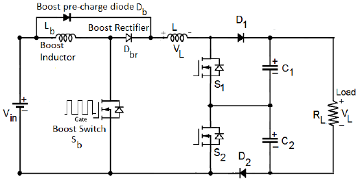
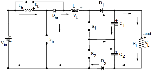
The configuration of a non-isolated positive output DC-DC boost converter with high voltage gain capability is shown in Figure 1. The suggested topology is the extension of the converter configuration given in (Balakishan et al., 2015) with boost power stage included. The converter is operated in continuous conduction mode. The proposed configuration employs passive components such as two identical inductors (Lb and L) each of 1 mH inductance, and two identical capacitors C1 and C2 each of 200 µF capacitance. The capacitors C1 and C2 are selected so that the balancing of voltage is achieved across the capacitors. The suggested topology is a double boost configuration. The first stage is a boost power stage consisting of boost switch (Sb), boost inductor (Lb), boost pre-charge diode (Db), and a boost rectifier diode (Dbr) with DC source (Vin). The second stage is another boost power stage comprising of power switches (S1 and S2), two ideal diodes (D1 and D2), and the capacitors C1 and C2 respectively. Each of the capacitors C1 and C2 receives half of the output voltage (V0) and are acting as filter capacitors to filter out the ripples in the DC output voltage and current. The ideal power switches (Sb, S1, and S2) are suitably triggered into conduction by proper gate pulses with duty ratio D = 0.8 for each switch. The switching frequency (fs) of the switches is taken as 50 kHz. The four distinct modes of operation of the converter are discussed as shown in Figure 2. The key waveforms of the converter configuration proposed are shown in Figure 3.
(d). Mode-IV (t3 < t < t4)
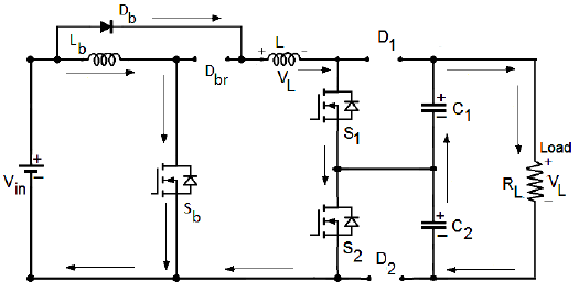
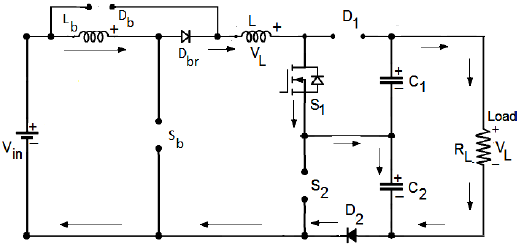
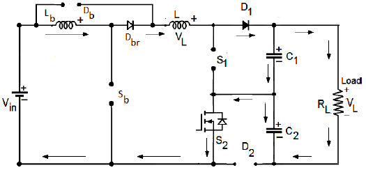
Figure 2 Modes of operation of the converter: (a). Mode I, (b). Mode II, (c). Mode III, (d). Mode IV.
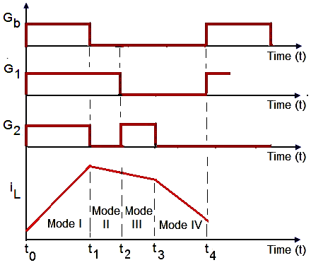
Figure 3 Key waveforms of the suggested converter for 0.5 < D < 1 during continuous inductor current mode.
2.1. Mode-I (t0 < t < t1)
The Mode I operation of the converter is depicted in Figure 2(a). In this mode, the switches Sb, S1, and S2 are turned ON. The diode Db gets forward biased. The diodes Dbr, D1, and D2 are reverse biased. The two inductors Lb and L are charged to the supply voltage Vin (>0) since they are connected in parallel. The two identical inductors Lb and L carry equal currents and they absorb the energy (WON) from the DC source. The charged capacitors C1 and C2 supply the load current. The current flow path is as indicated in Figure 2(a). The following equations are obtained during Mode-I operation:
Where,
2.2. Mode-II (t1 < t < t2)
During this time interval, the switch S1 remains in the turn ON mode. The switches Sb and S2 are turned OFF. The diodes Db and D1 are reverse biased. The diodes Dbr and D2 get forward biased. The current flow path is as indicated in Figure 2(b). The two inductors are connected in series. The voltage appearing across each inductor is given by Eq. 3.
This voltage level is so low that only small amount of energy is released from the inductors Lb and L through S1 and C2 for 0.5 < D < 1 as shown in Figure 3.
2.3. Mode-III (t2 < t < t3)
During this time interval, the switch S2 is turned ON. The switches Sb and S1 are turned OFF. The diodes Db and D2 are reverse biased. The diodes Dbr and D1 get forward biased. The current flow path is as indicated in Figure 2(c). The two inductors are connected in series. The voltage appearing across each inductor is given by Eq. 4.
This voltage level is also so low that only small amount of energy is released from the inductors Lb and L through C1 and S2 for 0.5 < D < 1 as shown in Figure 3. The voltage levels across the two inductors are equal during Mode II and III since
2.4. Mode-IV (t3 < t < t4)
During this mode, all the switches (Sb, S1, and S2) are turned OFF. The diode Db gets reverse biased. The remaining diodes are forward biased. The current flow path is as indicated in Figure 2(d). The two inductors are connected in series. The voltage appearing across each inductor is given by Eq. 5.
This voltage level is sufficiently high that major amount of energy is discharged from the inductors Lb and L through (i). the series combination of C1 and C2, and (ii). the load R0 as shown in Figure 3. The energy released (WOFF) by each inductor is given by Eq. 6.
According to the law of conservation of energy, the Eqs. 2 and 6 are equal. Hence, the voltage gain (G) of the proposed DC-DC converter is obtained as shown by Eq. 7.
3. Simulation results and discussion
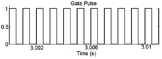
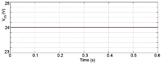
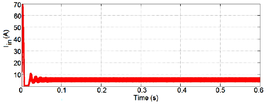
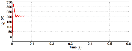
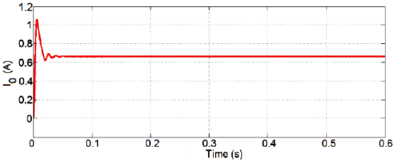
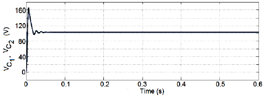
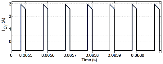
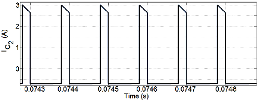
The MATLAB / SIMULINK model of the proposed non-isolated continuous inductor current mode operated three-level DC-DC converter with boost power stage is developed and is shown in Figure 4. The boost power stage consists of a power switch Sb, an inductor Lb, a diode Db, and a boost rectifier diode Dbr. The switching frequency (fs) for the converter is chosen as 50 kHz with duty ratio D = 0.8 for each switch. The values of converter parameters used for simulation are shown in Table 1. Each of the three switches (Sb, S1, S2) is triggered into conduction by applying the gate pulse as shown in Figure 5. The converter circuit is energized by a DC input voltage (Vin) of 24 V as shown in Figure 6. The current (Iin) delivered by the input DC source is as shown in Figure 7. With duty ratio D = 0.8 for each switch, the voltage obtained at the load end (V0) is around 208 V and the load current (I0) is nearly 0.66 A as depicted in Figure 8 and Figure 9 respectively. But, without the boost power stage, the output voltage (V0) is around 120 V and the corresponding output current (I0) is nearly 0.38 A for the same input DC voltage and duty ratio (Balakishan et al., 2015). Hence, the voltage conversion ratio as well as the output current of the converter proposed in this research work have been enhanced. The boost inductor (Lb) voltage and current waveforms are shown in Figure 10 and Figure 11 respectively. Similarly, the waveforms of voltage across and current through the inductor L are depicted in Figure 12 and Figure 13 respectively. The voltage stress and current stress of the power switches Sb, S1, and S2 are analyzed and the corresponding waveforms are shown in Figure 14, Figure 15, Figure 16, Figure 17, Figure 18, and Figure 19 respectively. This stress analysis illustrates that the switches are subjected to low voltage and current stresses compared to that for the conventional two-level boost converter. Hence, the switching losses are reduced in the proposed converter topology. The performance of the converter is validated by varying the duty ratio D of the switches from 0.6 to 0.9. The waveforms of voltages appearing across and the currents through the four diodes Db, Dbr, D1, and D2 are shown in Figure 20, Figure 21, Figure 22, Figure 23, Figure 24, Figure 25, Figure 26, and Figure 27 respectively. The analysis of waveforms of diodes indicates that the diodes are also subjected to low voltage-current stress. The waveform of voltages appearing across the two identical capacitors C1 and C2 is illustrated in Figure 28. The voltages are balanced across the capacitors. The sum of these two capacitor voltages is obtained as the output voltage (V0) at the load end. The charging and discharging current characteristics of the capacitors C1 and C2 are shown in Figure 29 and Figure 30 respectively.
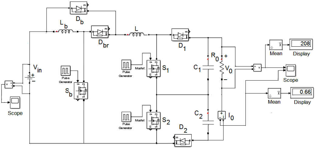
Figure 4 MATLAB / SIMULINK model of the proposed non-isolated DC-DC boost converter with boost power stage.
Table 1 Parameters of the proposed converter for simulation.
| Parameters | Symbol | Value |
|---|---|---|
| Input DC voltage (V) | Vin | 24 |
| Output DC voltage (V) | V0 | 208 |
| Inductors (mH) | Lb, L | 1 (each) |
| Capacitors (µF) | C1, C2 | 200 (each) |
| Switching frequency (kHz) | fs | 50 |
| Load resistance (Ω) | R0 | 311 |
| Output DC current (A) | I0 | 0.66 |
| Duty ratio for each switch (Sb, S1, S2) | D | 0.8 |
4. Prototype model of the converter
The prototype model of a rectifier-fed DC-DC converter based on double boost topology capable to deliver 100 W output power has been developed and is as shown in Figure 31. The double boost topology includes all components of three-level configuration shown in Figure 1, except the switch S2 and the capacitor C2 (Liu et al., 2020). However, the voltage gain (G) equation is same for both the double boost topology and the three-level topology proposed in this work. The low power hardware model is designed to provide an output DC voltage of around 108 V at the load end for an average DC input voltage of around 12 V at the rectifier end. The power MOSFET switches are made to operate at duty ratio D = 0.8. The model employs an Integrated Circuit (IC) chip named as KA3525A PWM controller incorporating the control circuitry for the generation of pulse width modulated (PWM) signals for the MOSFET switches Sb and S1. The PWM controller KA3525A is a 16 pin chip that requires a supply voltage of 40 V and features a reference output current of around 50 mA. It incorporates an error amplifier, voltage reference, a pulse width modulator, an undervoltage lockout, an oscillator, the output driver, and a soft start circuit, all in one package.
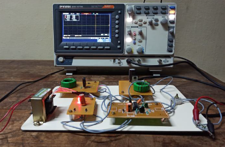
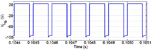
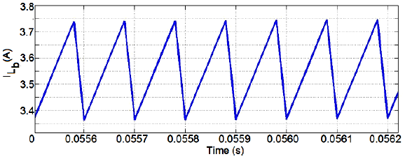
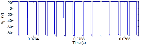
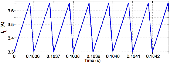
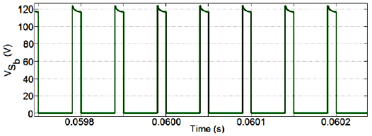
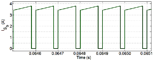
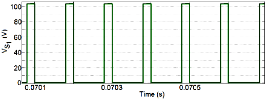
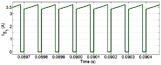
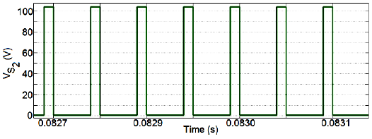
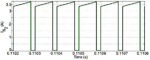
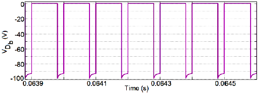
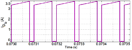
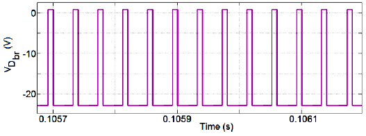
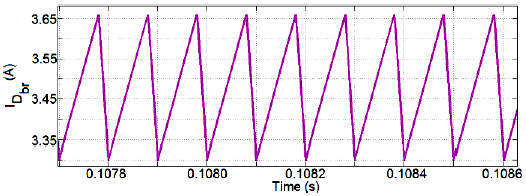
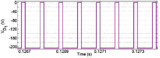
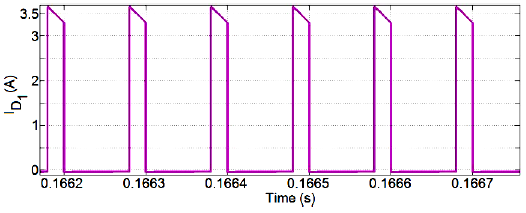
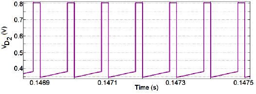
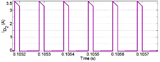
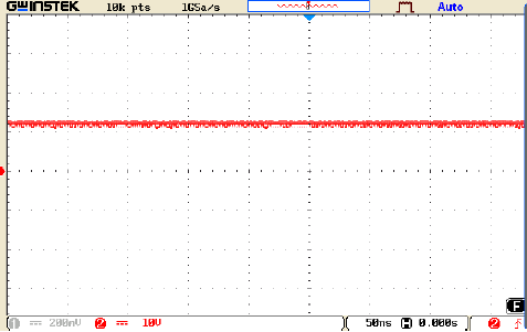
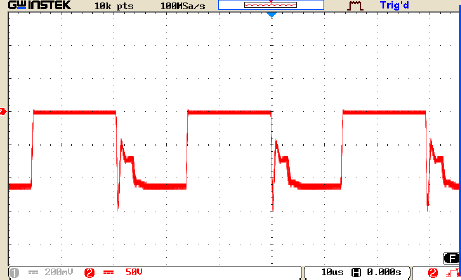
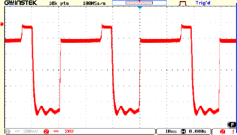
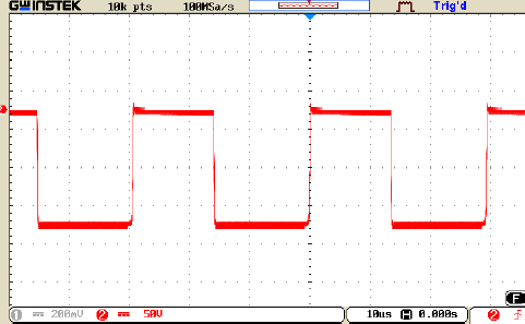
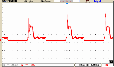
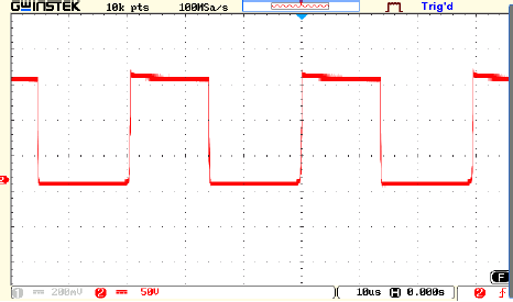
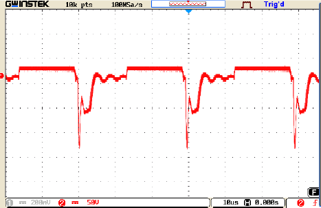
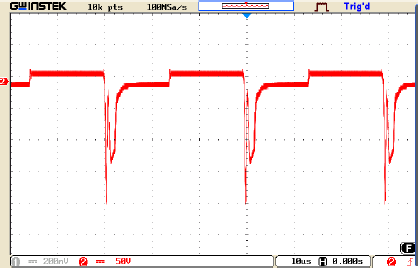
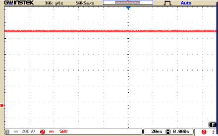
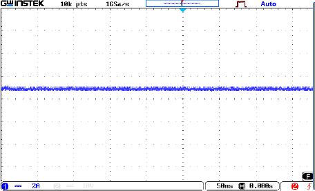
The power switches are turned ON and OFF simultaneously as per the gate pulse waveforms shown in Figure 32. The values of components of the hardware model of the converter are listed as shown in Table 2. The actual waveforms, taken on digital storage oscilloscope (DSO), for all internal components and power switches are shown in Figure 33, Figure 34, Figure 35, Figure 36, Figure 37, Figure 38, Figure 39, Figure 40, Figure 41, and Figure 42 respectively.
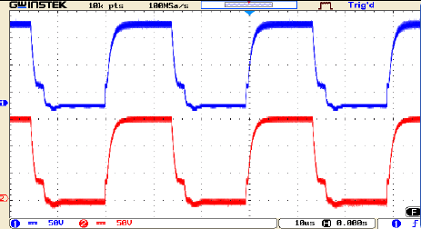
Table 2 Components of the hardware model of the DC-DC converter.
| Circuit components | Description | Type |
|---|---|---|
| Sb , S1 | Power MOSFETS | IFR640N, 200 V, 18 A |
| Db, Dbr, D1 | Diodes | DFE10I600PM, 600 V, 10 A |
| Lb, L | Inductors | 0.35 mH each |
| C1 | Capacitor | 47 µF |
| fs | Switching frequency | 30 kHz |
| R0 | Load resistance | 100 Ω |
| P0 | Output power | 100 W |
| I0 | Output current | 1 A |
5. Conclusions
In this paper, the steady state analysis of a non-isolated continuous input current positive output three-level DC-DC converter with boost power stage has been carried out. The validation of the performance of the proposed converter is done by simulating the converter in MATLAB / SIMULINK platform. The voltage and current waveforms for all the active and passive components of the converter are presented for duty ratio D = 0.8. The simulation results illustrate that the voltage gain of the proposed simple three-level DC-DC converter structure with boost power stage can be improved by (1+D) times that of the traditional three-level / boost configured DC-DC converter. The prototype model results are also provided to validate the theory and the time domain results. The additional features of the converter configuration proposed in this work are that the MOSFET switches are subjected to low voltage and current stresses thereby reducing the switching losses and hence improving the overall efficiency of DC-DC conversion. The diodes too experience low voltage-current stress. The filter components C1 and C2 are so chosen that the output voltage and current waveforms have only fewer amounts of ripples. Moreover, the output voltage and current waveforms settle down to steady state values after executing only few oscillations. The proposed converter is well-suited for renewable energy applications that require high voltage. Future work may include the application of the zero-voltage-switching concept to the active switches for switching loss reduction in the view to enhance the overall conversion efficiency.
Conflict of interest
The authors do not have any type of conflict of interest to declare.
Financing
The authors did not receive any sponsorship to carry out the research reported in the present manuscript.

