


 text new page (beta)
 English (pdf)
 Article in xml format
 Article references
 Send this article by e-mail
 Cited by SciELO
  Similars in
SciELO
Similars in
SciELO 
 Permalink
1. INTRODUCTION
Indium based solders have distinct features of low melting temperature and low temperature ductility. The low soldering temperature of indium based solders make them excellent choice for temperature sensitive thin film transistors (Chao-Nan & Jung-Jie, 2015). They have very rapid rate of recovery and recrystallization, which could be as fast as their work hardening rate. These characteristics make the indium joint seldom to fail under thermal cycling: usually they fail due to overload or unidirectional creep (Goldstein & Morris, 1994). Therefore, indium solders could be a preferred choice to solder dissimilar materials to be used under thermal cyclic service condition (Darveaux, Banerji, Mawer, & Dody. 1995).
Pure indium has low wetting and spreading characteristics along with mediocre mechanical strengths, therefore usually is not a choice of soldering materials with gold. However, above mentioned characteristics could be ameliorated by the incorporation of alloying elements like: Sn, Pb, Ag, or Bi. Alloy addition effectuates formation of eutectic phase(s) rendering certain practical benefits. Primarily, the alloying causes formation of multiphase microstructure, which improves the mechanical properties of the solder. Moreover, the alloying supports the formation of mixed-composition oxides of indium and alloying element(s), which could be easily removed using a flux, otherwise, puré indium forms a sticky and persistent oxide film, which is difficult to remove using general purpose fluxes. Indium based solder are more expensive than their competitors (1:80 times), however they offer following characteristics, making them a choice
for high-valued applications (Indium Corporation, 2016):
Indium is ductile and malleable which allows it to deform and fill in the uneven structure of two mating parts, using only modérate pressure.
This ductility and malleability are retained at cryogenic temperatures so that an assembly can maintain an effective seal, even in harsh environments.
With a relatively high thermal conductivity of 86 W/mK at 85 °C, indium is widely used in thermal management applications to dissipate the heat produced by electronic components.
Indium compensates for different coefficients of thermal expansión when bonding dissimilar parts.
Offers improved thermal fatigue of solder in electronics assembly.
Indium solders may have low melting temperatures (<180 °C), making them ideal for step soldering or applications that require lower reflow temperatures.
Indium has a low vapor pressure, making it suitable for use in high vacuum applications.
Indium alloys enable solders to withstand drop tests better than other low melting alloys.
Indium based solders have a major application for joining gold coated components and electrical tracks. The primary reason is the restricted solubility of gold in indium, while other solders readily dissolve gold at soldering temperatures. The dissolution continúes till the depletion of gold under the solder occurs making the joint vulnerable to low mechanical strength and insufficient electrical conduction. Contrarily, indium forms an intermetallic compound (Auln2), also known as scavenging phase, at the interface of gold (Yost, Ganyard, & Karnowsky, 1976). If the compound forms a continuous layer on the interface of gold, further dissolution of gold is restricted. The formation of continuous intermetallic layer is supported by selective alloy additions e.g. silver. In the presence of silver, the interfacial layer takes the form of continuous grains of the Auln2 compound embedded entirely in primary indium. The silver restricts facile diffusion between the solder and the gold coating, therefore limiting the reaction to continué (Jacobson & Humpston, 1989).
Moser et al. (2001) presented their work incorporating development of Ag-In phase diagram and surface tensión of various phases and compositions of the alloy.
They found that indium forms five binary compounds with silver from 227 to 1170 °C. It was also observed that surface tensión of indium increases with the addition of silver. In 2004, Yoon et al (Kim et al., 2004) studied the characteristics of high temperature In-Ag solder using diffusion bonding. They found that with varying amount of silver, diffusion bonded joints may withstand wide range of operating temperatures i.e. from 270 to 700 °C. Similarly, Chang et al. (Chang & McCluskey, 2009) studied the reliability of indium solder at cryogenic temperature. They recommended the use of indium solder for as low as -150 °C temperature with consistent characteristics of electrical and thermal conductivity, ductility and mechanical strength.
As discussed above, different research groups have studied various composition of the In-Ag solders along with their characteristics but quite limited information about the wetting and interfacial characteristics of eutectic In-Ag solders is available. In present work, three homogeneous eutectic In-Ag solders were prepared i.e. hypo-eutectic, eutectic and hyper-eutectic using melt-cast route. These solders were investigated for compositional homogeneity, phase analysis, melting temperature, microstructure, wetting and spreading characteristics and compared with puré indium. Tendency of the solders towards the formation of scavenging phase (Auln2) was also investigated and discussed for reliable solder joints.
2. Ag-In PHASE DIAGRAM
A typical Ag-In phase diagram is shown in Figure 1, where seven equilibrium phases exist, out of which two are intermetallic phases i.e. Ag2In and Agln2 also known as (φ) and γ phases, respectively (Okamoto, 2010).
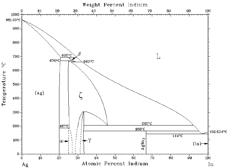
The silver solid solution of Ag-In has solubility of indium up to 21 wt. % with a wide temperature range. Contrarily, the indium rich solid solution has lower solubility of silver i.e. -1.0 wt. % of silver. At eutectic point of 144 °C, a eutectic reaction occurs at 97 wt. % of indium. At room temperature, alloy with indium composition above 68.1 wt. % is a mixture of puré indium and indium rich intermetallic compound (i.e. φ phase) with a solidus temperature of 144 °C. Above this temperature the alloy converts to a mixture of liquid phase and intermetallic (φ) phase, which begins to decompose into liquid phase and the γ phase. With increasing temperature, the mixture transforms into liquid and γ phase until 205 °C temperature reaches. At eutectic point (i.e. 3.0 wt. % of silver at 144 °C) fully eutectic Ag-In phase exists, however above or below to this composition hyper- or hypo- eutectic alloys are formed, respectively.
3. EXPERIMENTAL
High purity elemental indium and silver metáis were used as constituent materials of the alloys. Three alloys were prepared having 2.5, 3.0 and 3.5 weight percent silver designated as hypo-eutectic, eutectic and hyper-eutectic alloys, respectively. To replenish indium losses during alloy making, a 1.5% allowance was added for charge calculations. The alloy making sequence was as follows: first pre-weighed indium shots were placed in an alumina crucible and heated to 165 °C. After complete melting of indium, pre-weighed silver filings were added in the melt and stirred with stainless steel spatula. The temperature of the melt was raised to 185 °C and the melt was kept on stirring for 10 minutes. Subsequently, the alloy was cast into copper mold. To homogenize the alloys, the ingots were cold rolled to >90% reduction in thickness and re-melted at 180 °C for 10 minutes and cast into copper mold. Finally, the ingots were again cold rolled to >70% reduction in thickness and preserved for subsequent characterization and evaluations.
All the three alloys were subjected to energy dispersive spectroscopy (EDS) and inductively coupled plasma (ICP) analysis for determination of the final compositions of the alloys as well as their homogeneity.
The phase analysis of the alloys was carried out using a Jeol X-ray diffractometer with a Cu-Ka radiation source. The full sean was carried out from 20° to 100° - 2θ range with a step size of 0.05 degree/sec.
The effect of silver addition on melting temperatures of the soldering alloys was determined using differential scanning calorimetry (DSC) in argón environment with a heating rate of 10 °C/min. For each alloy, 5 mg of the specimen was used and the same DSC eyele was repeated twice to ensure the repeatability of the thermal response.
Microstructural analysis of the alloys was carried out using optical microscope in diffractional contrast illumination mode. The surfaces of rolled alloy strips were cold mounted and chemically polished using 20% citric acid solution at 45 °C for 30 minutes. After polishing, the specimens were etched in 15% solution of nitric acid for 60 seconds.
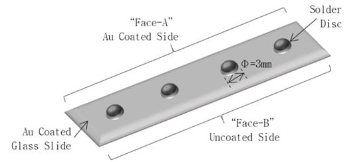
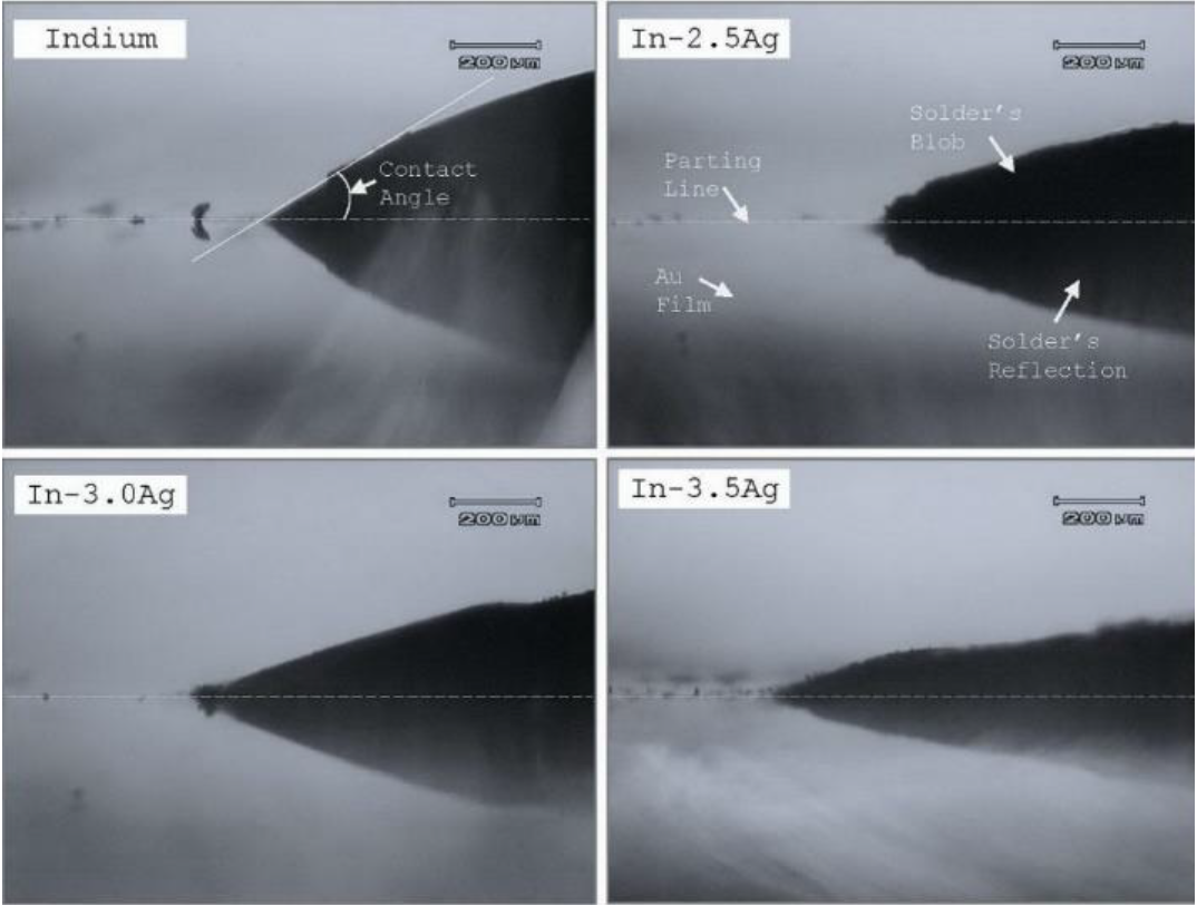
Wetting behavior of an alloy has prime importance for soldering process. To study the behavior; disc specimens having equal size and dimensión (φ=3 mm, thickness= 0.3 mm) were prepared out of different solders using a dye punching machine. A 200 nm thick gold film was deposited on a cleaned glass slide using a thermal evaporation unit. The solder dises were placed on the gold coated glass slide at equal distance and heated in a furnace at 170 °C for 100 seconds. Wetting angles were measured using an optical microscope in transmission light mode at "Face-A" of the glass slide, while the extent of scavenging phase (Auln2) formation was studied at "Face-B" of the glass slide using optical microscope in reflection light mode. Additionally, dissolution phenomena of gold in indium (i.e. the scavenging), resulting in the formation of Auln2 phase, were studied at "Face-A" using scanning electrón microscope for better resolution and evaluation. The slide faces for different study modes are schematically demonstrated in Figure 2.
4. RESULTS
4.1 MATERIAL CHEMISTRY AND HOMOGENEITY
Prior to chemical analyses, the rolled strips of the alloys were cleaned using mild solvents. The results are given in Table 1. It could be observed from the results of chemical analyses that all the three alloys have a narrow tolerance with the required concentration of silver. There were some impurities like copper and zinc in the alloys in low concentrations. To confirm the homogeneity of the alloys, múltiple analyses were carried out for each specimen i.e. at least three analyses for each specimen. The results were then averaged out and standard deviation of the individual alloy was calculated. The valúes of the standard deviations show extant of alloys' homogeneity.
4.2 X-RAY DIFFRACTION
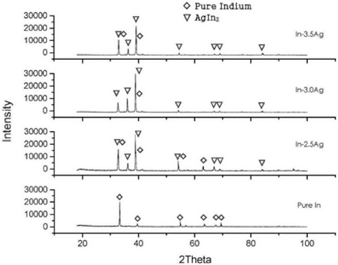
The main purpose of XRD analysis was to determine the formation of eutectic phase, which is basically a structure comprising indium matrix and the intermetallic compound Agln2. In Figure 3, XRD scans of various solder materials are superimposed along with peak identification for indium and Agln2. PDF No. 01-1042 and PDF No. 25 0386 data cards were used to identify the corresponding peaks of the indium and the intermetallic compound, respectively. It could be seen in XRD scans that intermetallic compound was dominantly formed in the alloys. No peaks representing free silver were present in the scans, which is an evidence of the homogeneous formation of the alloy.
4.3 DIFFERENTIAL SCANNING CALORIMETRY
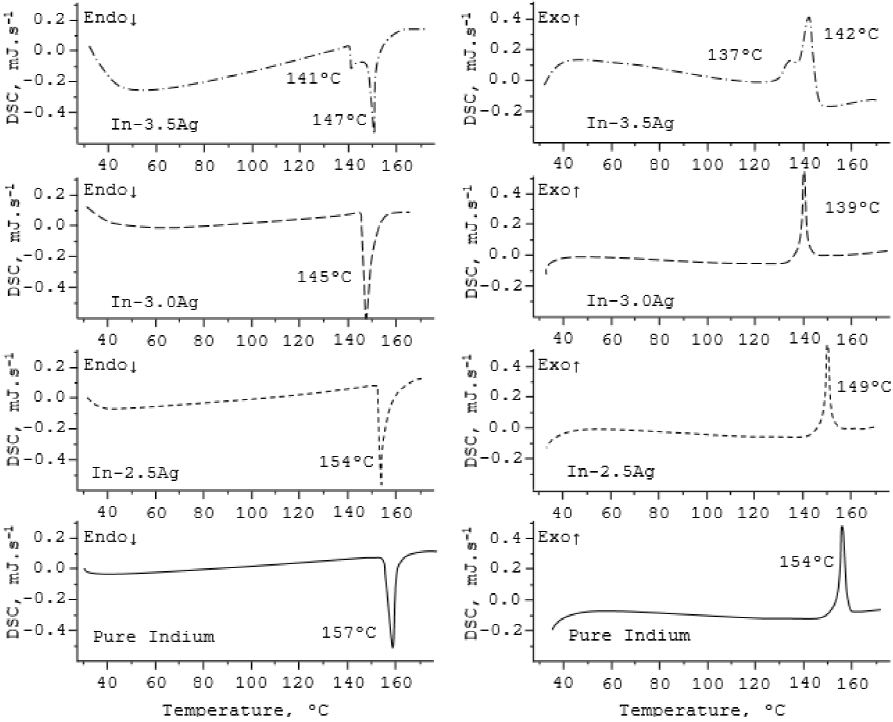
Figure 4 shows the DSC heating and cooling curves for the specimens under investigations i.e. puré indium, In-2.5Ag alloy, In-3.0Ag alloy and In-3.5Ag alloy. During DSC cycling, TGA plots were also drawn (not shown in Figure 4), where it was observed that all the materials under test did not undergo any weight loss. DSC heating curve of pure indium has a sharp endothermic peak (at 157 °C), which is a characteristic melting feature of pure elements, while its cooling curve exhibited 3 QC drop (i.e. 154 UC), which indicates the presence of minor impurities. However, for the eutectic alloys the peak width increased with the addition of silver. The melting points for hypo-, hyper- and eutectic alloys were 154, 147 and 145 °C, respectively. Due to the presence of silver alloying in indium, the solidification temperatures of the alloys varied from melting points i.e. 149, 139, 142 C for In-2.5Ag, In-3.0Ag and In-3.5Ag alloys, respectively. No other thermal variations were observable in the curves depicting the fact that alloys were homogeneous with feeble impurity levéis, which were beyond the detection limit of DSC apparatus. However, the DSC curve of hyper-eutectic alloy was accompanied by an additional endothermic peak (at 141 °C), which was relatively smaller than the melting peak. This peak was due to excess crystalline eutectic phase present in the alloy (Diaz, 2005).
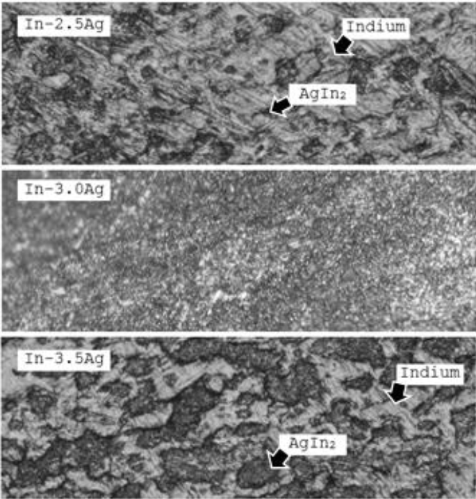
4.4 MICROSTRUCTURE OF THE ALLOYS
As the alloys were cold rolled into strips after the casting, no dendritic features were seen in the microstructures (Figure 5). Additionally, no sign of cold working was present in the microstructure because indium has a very high recovery and recrystallization rate even at room temperature (Darveaux, 1995). The structure was primarily eutectic intermetallic of indium and silver (Agln2) accompanying primary indium matrix. The hypo-eutectic alloy contained relatively more primary indium matrix as compared to the hyper-eutectic alloy. The microstructure of In-3.0% Ag alloy was fully eutectic in appearance with a negligible presence of primary indium matrix, which depicted the homogenized formation of the alloy.
4.5 WETTING AND SCAVENGING
It is believed that the easy and extended wetting of a surface by any liquid phase is manifested by the lowest contact angle made by the liquid drop resting on the surface. Generally speaking, any contact angle below 90° will have the characteristics of wetting, however perfect wetting could be achieved at as low as 0° contact angle. The reduced contact angle is basically a function of surface tensión forces of the two mating surfaces. A lesser difference in the surface tensión forces will favor the formation of lower contact angles (Silva, Cheung, Garcia. & Spinelli, 2015). In the present study, when the solder alloys were in liquid form during soldering, various contact angles were expected due to the addition of silver, as the surface tensión of indium, silver and gold are 556 mN.m1, 925 mN.m^and 1145 mN.m1, respectively (Keen, 1993). The effect of silver contents in indium was accordingly with respect to contact angles (Figure 6). Puré indium exhibited 38° contact angle with gold, which reduced to 29.4°, 23.7° and 19.5° with the addition of 2.5, 3.0 and 3.5% silver, respectively. A máximum decrease in contact angle up to 49% was observed with 3.5% silver alloying. The decrease in contact angle was rapid up to 3.0% silver addition, which became sluggish for subsequent addition.
Another wettability index of solder alloys is their "spreading factor", which is the property of the solder to flow in liquid state and is related to the contact angle. Some researchers have previously investigated the correlation between contact angle and spreading factor of the solders; Eq-1 is a mathematical expression of such a correlation (Takao, Tsakada, Yamada, Yamashita, > Hasegawa, 2009) :
where, (ϕ) is the experimental valué of contact angle in degrees and ƞ is calculated value of spreading factor in percentage.
The calculated results showed that the puré indium has -75% spreading factor, while increasing silver contents (up to 3.5 %) improved the factor to > 90%. However, it is noticeable that the increase was rapid until eutectic composition and afterwards it became steady. The spreading property of eutectic alloys is well known, which is indeed the primary reason why majority of the solders have eutectic compositions besides the single transformation temperature i.e. liquid to solid phase (Wei. Wan, Xue, & Wang, 2011). High spreading factor is desirable in certain applications where a solder slug is applied to a heated substrate and expected to flow and fill the joint under capillary action. Contrarily, in applications where a solder foil is sandwiched between two components which are to be joined together using an appropriate thermal cycle; a high spreading factor of a solder might be detrimental because the molten solder will tend to flow out of the joints, making unwanted electrical connections and subsequent electrical leakage.
Besides wetting and flow characteristics, the scavenging zones of the solder alloys with gold thin film were studied using SEM. Here it should be worth mentioning that the Figure 7 is the topographic montage of the solders and gold film at "Face-A" and Figure 8 is the interphase montage of "Face-B" as demonstrated in Figure 2.
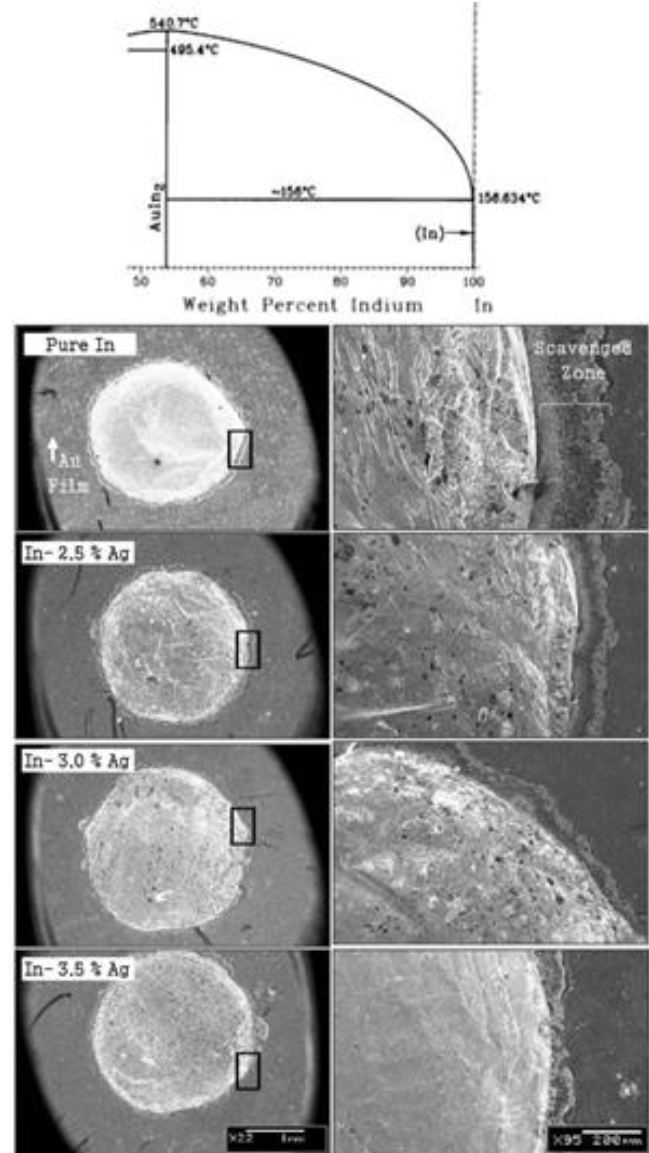
Fig. 7 Eutectic segment of In-Au phase diagram showing the formation of scavenging phase. Others are SEM micrographs of various solder alloys demonstrating reductions in scavenging zone with silver contents.
SEM Observations at "Face-A ": Indium and gold has a tendency to form intermetallic compound (i.e. Auln2) at as low temperature as melting point of indium (part of the phase diagram is shown as an inset at top of Figure 7), which makes the solder joint prone to low strength and high electrical noise, for example in case of sensor applications. In Figure 7, it could be seen that puré indium solder has formed a large scavenging zone comprising Auln2 with gold. The width of the zone is more than 228 µm, however it reduced drastically with the addition of silver i.e. 109, 52 and 47 µm for 2.5, 3.0 and 3.5 % addition, respectively. Smaller scavenging zones ensure the presence of metallic gold thin film beneath the solder, providing better electrical and mechanical properties of the contact.
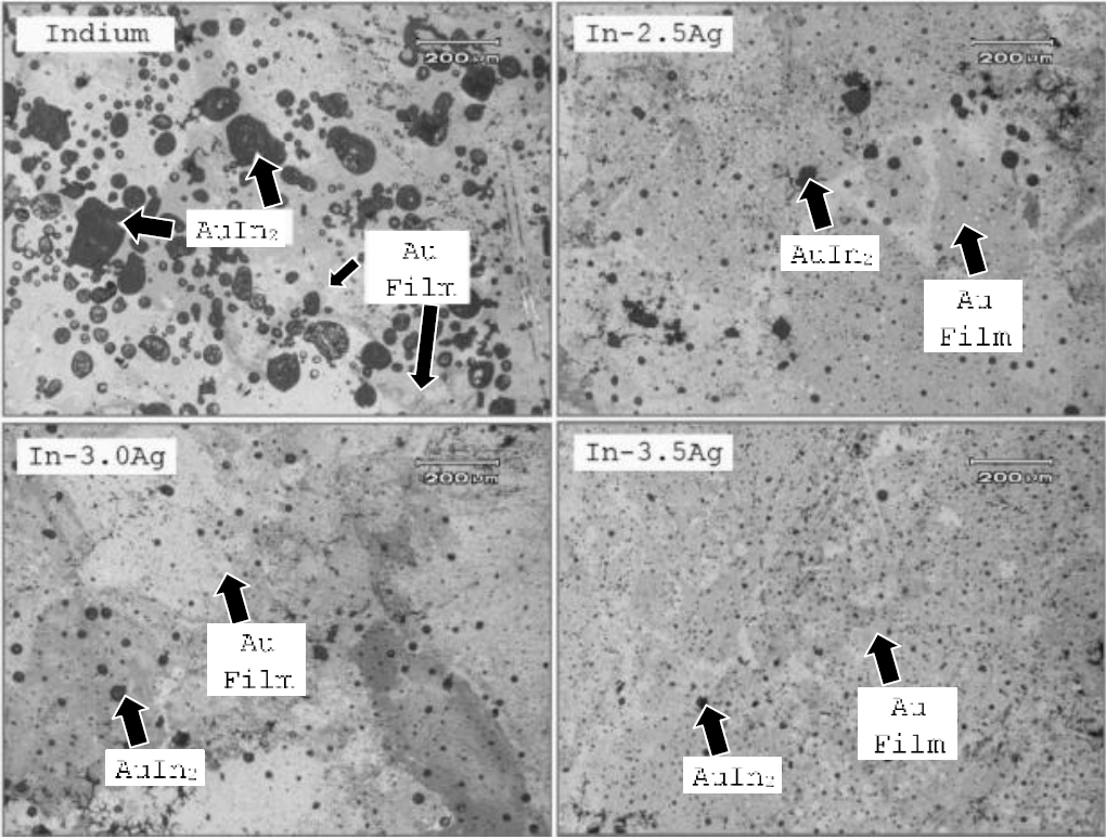
SEM Observations at "Face-B": These observations were made to evalúate the extent of scavenging behavior of under investigation solders with gold thin film. Puré indium formed large island of Auln? phase with the film. These islands had spherical geometry depicting the fact that the molten indium initially formed a tiny molten nucleus of Auln2 phase, which subsequently grown to the large molten mass during the thermal process. Formation of scavenging phase reduced appreciably with the addition of silver and an optimal reduction was observed at 3.5% silver contents (Figure 8). An interactive software (OLYSIA-M3) was used to quantify Auln? phase in various solder alloys. The percentage of the phase was 41.2, 22.7, 17.3, and 11.9 for puré indium, In-2.5%Ag, In-3.0%Ag and In-3.5%Ag alloys, respectively.
5. DISCUSSION
Alloy preparation method, as described in the experimental section, seems to be an effective approach for homogeneous distribution of constituent elements. Material analysis through EDS and ICP depicted the uniform distribution of the constituent elements. Additionally, XRD and microstructural analyses showed the consisteney of phase distribution; no evidence for the presence of elemental silver and/or segregation was found. Complete formation of various phases and their uniform distribution within an alloy play a vital role towards the subsequent performance of the alloy i.e. how the alloy will perform with respect to its physical and mechanical properties. Hence, uniform and consistent melting temperatures of the alloys were observed during DSC studies, which were in conformation with In-Ag phase diagram (Okamoto, 2010).
Apart from the findings of chemical analyses, XRD and microscopy, the results of contact angle measurement, spreading factor, scavenging zone and fraction of Auln2 phase were graphically presented in Figure 9. It could be seen that addition of silver affected all the characterized properties of the various solder alloys. As contact angle and spreading factor are inversely proportional to each other; the addition of silver (-3.5% max.) in indium reduced the contact angle up to 49% resulting a raise of 21% in spreading factor. These two parameters reflect the wettability of the solder with gold thin film i.e. lower the contact angle and higher the spreading factor for better wetting (Chang & McCluskey, 2009). The change in wetting properties of indium solder is driven by the formation of Agln2 phase, which reduced the surface tension forces of the solder in molten state.
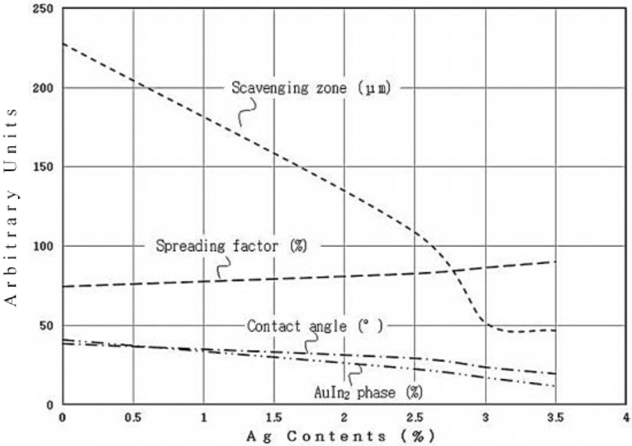
Fig. 9 Effcct of silver addition on contact angle, spreading factor, scavenging zone, and amount of Auln2 phase during soldering.
During the soldering, formation of Auln2 phase increased the extent of the scavenging zone i.e. more the quantity of Auln2 phase more the depletion of gold from the substrate. The addition of silver in indium reduced, up to 77%, the formation of Auln? phase, which displayed a direct effect on the decrease of scavenging zone in the corresponding ratio. During soldering of gold substrates using indium solders, better mechanical and electrical contaets can be made if the scavenging zone has a restricted growth (Chang & McCluskey, 2009)). Experimental results showed that silver addition to indium solder had reduced the formation of Auln2 phase i.e. more the silver contents lesser the Auln2 phase. During soldering to gold substrates, presence of silver in indium helps the formation of a continuous layer of Auln2 phase acting as a barrier to restrict the dissolution of gold from the substrate, thence limiting the scavenging zone (Humpston & Jacobson, 2004).
5.1 CHOICE OF THE SOLDER
A prudent selection of the solder for gold thin films (200 nm) could be made based upon various experimental results of the present work; for which numerical valúes are shown in Table 2. An obvious choice could a solder having a máximum quantity of silver i.e. 3.5%Ag; reflecting minimum contact angle besides other ameliorated wetting and soldering characteristics. However, such a solder may suffer issues like delayed soldering action, sequential solidification and compromised strength due to a range of temperature for melting and solidification (141 to 147 °C). Contrarily, the eutectic alloy (3.0%Ag) executed comparable wetting and soldering characteristics along with single melting temperature (145 °C), which in turn offers better soldering practice with promising electrical and mechanical properties.
Table 2 Effect of Ag addition on contact angle, spreading factor and scavenging phase.
| Pure In | In-2.5 % Ag | In-3.0 % Ag | In-3.5 % Ag | Change | |
| Melting temp. (°C) | 157 | 154 | 145 | 141-147 | - |
| Contact angle | 38.8° | 29.4° | 23.7° | 19.5° | - 49% |
| Spreading Factor | 74.48 | 82.82 | 86.62 | 90.34 | + 21% |
| (%) | |||||
| Scavenging Zone | 228 ± 14 | 109 ± 17 | 52 ± 12 | 47 15 | - 79% |
| (Hm) | |||||
| Aulm phase (%) | 41.2±3.2 | 22.7±1.7 | 17.3±2.1 | 11.94=1.9 | - 77% |
6. CONCLUSIONS
Following conclusions were drawn from the present work:
Addition of silver to the indium solder reduced the melting temperature, contact angle, size of the scavenging zone and quantity of the Auln2 phase, which can contribute towards better electrical and mechanical characteristics of the soldering joint with gold thin films.
Silver addition also improved the spreading factor of the solder, making it a choice of material for soldering-slug based soldering.
CONFLICT OF INTEREST
The authors have no conflicts of interest to declare.

