


 nueva página del texto (beta)
 Inglés (pdf)
 Artículo en XML
 Referencias del artículo
 Enviar artículo por email
 Citado por SciELO
  Similares en
SciELO
Similares en
SciELO 
 Permalink
1. Introduction
In recent years, the development of transparent electronics has achieved considerable progress since wearable electronics, transparent circuitry, e-paper, solar cells and more (Bashir et al.,2009; Langley et al., 2013; Zhu, Fang, Preston, Li, & Hu, 2014).Although the recent development in thin-film transistors (TFTs)has been very important to enable this technology, it is necessary to develop other basic devices such as transparent capacitors.These basic devices could work as sensors, energy storage from solar cells, memory devices and charge-discharge capacitors inactive-matrix displays could also be very useful to analyze the quality of the dielectric-semiconductor interface in field effect devices (Khan, Bhansali, & Alshareef, 2011; Xian & Yoon,2009; Yu, Li, Zhang, Sun, & Zheng, 2015; Zhang et al., 2015).
The use of transparent electrodes is key for developing transparent electronic devices, in which indium tin oxide (ITO) has been most commonly used. However, because of the high demand of indium, the use of ITO will be economically unviable. Therefore, much research is under development to find alternatives to ITO. On the other hand, in addition to the unviability of ITO, the typically used deposition techniques involve high vacuum, present incompatibility with large-area substrates and high-cost. For these reasons, solution-process techniques have become very attractive because of their low-cost, simplicity, compatibility with large-area substrates and the film deposition under ambient conditions. It is important to mention that the consecutive solution-deposition of thin films to fabricate semiconductor devices has been a great challenge (Hunter et al., 2015). In this work, we present fully solution-processed zinc oxide metal-insulator-semiconductor (MIS) capacitors employing the ultrasonic spray pyrolysis andspin-coating techniques. Fluorine tin oxide and spin-on glass are used as transparent electrode and dielectric film, respectively.
2. Experiment
The films were deposited using a typical homemade ultrasonic spray pyrolysis (USP) deposition system adapted from an ultrasonic humidifier (Heaven Fresh). The transparent electrodes were obtained using fluorine tin oxide (FTO) from 0.2 Mp recursor solution of tin tetrachloride pentahydrate in etanol with ammonium fluoride diluted in deionized water prepared with F/Sn ratio of 0.52. The ZnO was obtained using 0.2 Mprecursor solution of zinc acetate in methanol. The transparent dielectric was obtained using a spin-on glass solution (SOG700B Filmtronics) diluted 3:1 with deionized water (DI) and spincoated onto the samples (Dominguez, Rosales, Torres, Moreno,& Ordu˜na, 2012; Dominguez, Obregon, & Luna-Lopez, 2016).
The orientation of the film was investigated using an X-ray diffractometer (XRD) (Discover D8-Bruker AXS) at 2θ range between 20o and 70o and 0.002o step. For the photo luminescence spectroscopy, a laser of He-Cd with 325 nm line was used asexciting source. The photoluminescence measurement was performed using a silicon PIN Thorlabs (DET-210) detector with a spectral response of 200-1100 nm. The conventional lock-intechnique was employed seeking to minimize the effect of noise.The voltage signal was acquired with a Computer Boards CIO-DAS08 data acquisition card, which operates in conjunction with a stepper motor controller to position the monochromator Sciencetech 9040 to the appropriate wavelength.
The IR absorption spectra of the films were measured witha Brucker FTIR Vertex-70 spectrometer. The IR spectrum was observed for wave numbers between 3500 and 400 cm−1.
To fabricate the transparent MIS capacitors, glass slides were used as substrates. The glass substrates were chemically cleaned.First, they were cleaned in acetone for 10 min, followed with isopropyl alcohol, also for 10 min, in an ultrasonic bath. Finally, the substrates were rinsed with deionized water. After that, FTO deposited by USP was used as bottom transparent electrode.Then, the SOG/DI dielectric film was spin-coated onto the samples at room temperature at 3000 rpm for 30 s. The samples were annealed at 100oC for 15 min to reduce humidity and evaporate most of the solvents, to finally be annealed for 5 h at 200oC inair ambient. Afterwards, as active layer, ZnO was deposited byUSP using air as carrier gas at flow rate of 467 sccm on a hot-plate at 200oC. Finally, FTO was deposited by USP as the top transparent electrode through a shadow mask. The MIS capacitors have an area of 0.002 cm2 (1 mm × 0.2 mm). The thickness of the ZnO and SOG/DI films was 350 ± 15 nm and 44 ± 5 nm, respectively.
The capacitance-voltage characteristics were measure dusing the Keithley-4200 semiconductor characterization system equipped with the 4200-CVU integrated C-V, under dark conditions, air ambient and room temperature. The measurements here reported are representative of 9 capacitors. The measurements present a fluctuation lower than the ±10% on the accumulation capacitance and breakdown voltage.
3. Results and discussion
Fig. 1 shows the schematic cross section of the ZnO MIS capacitors and a top-view photograph of the MIS capacitors.The MIS capacitors are highly transparent, which makes their use feasible in transparent electronics.
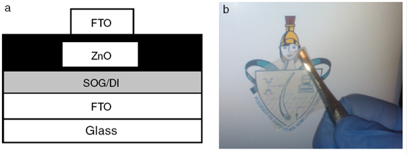
Fig. 1 ZnO MIS capacitor structure. (a) Schematic cross section and (b) photograph of the fabricated devices.
Fig. 2 shows the XRD pattern of the ZnO film. The peaks related to the planes (100), (002), (101), (102), (110), (103) and (112) can be identified according with the JCPDS Card No.36-1451, where the strongest peak is associated to the (100) plane. The XRD diffractogram shows a polycrystalline nature regardless of the low deposition temperature.
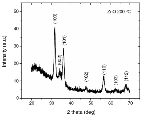
Fig. 3 shows the room temperature photoluminescence (PL) spectra of the ZnO film. It shows a PL spectrum with a peak centered at 390 nm and a high intensity broad band from 450 to 700 nm. The UV emission peak at 390 nm is associated with thenear band-edge (NBE) emission of the wide gap attributed tothe recombination of the free excitons (Padilla-Rueda, Vadillo,& Laserna, 2012; Sepulveda-Guzman et al., 2010; Xiao, Zhao,Liu, & Lian, 2013). The visible emission broad band from 450 to 700 nm includes the defects and impurities, which are consider-able in our case. The origin of this visible emission band may be attributed to oxygen vacancies, zinc vacancies, oxygen antisites,zinc antisites, oxygen interstitial and zinc interstitial (Janotti &Van de Walle, 2007; Lin, Fu, & Jia, 2001; Wang et al., 2006).

Fig. 4 shows the FTIR spectra of the ZnO film. The peakcan be observed at 415 cm−1 related to Zn O stretching modes (Adamopoulos et al., 2011; Gayen, Sarkar, Hussain, Bhar, &Pal, 2011). The peak at 1627 cm−1 is attributed to O H bending modes. Also, the peaks at 2500-3500 cm−1 are due to C H and O H stretching modes (Adamopoulos et al., 2011; Gayen et al.,2011). The peaks at 1413 cm−1 and 1530 cm−1 are attributed to C O stretching modes, while at 1750 cm−1 they are attributed toC O bonds (Adamopoulos et al., 2011; Gayen et al., 2011). The presence of C O bonds suggests an incomplete precursor pyrolysis due to the low deposition temperature (Adamopoulos et al.,2011). However, the characteristic Zn O band, approximately at415 cm−1, indicates the ZnO formation. On the other hand, it is important to mention that bonds related to O H stretching have been previously reported in ZnO films, indicating the presence of O H complexes that are associated with different defects and increased free-carrier concentration (Adamopoulos et al., 2011;Gayen et al., 2011; McCluskey, Jokela, Zhuravlev, Simpson,& Lynn, 2002; Shi et al., 2005). This agrees with what was observed in the photoluminescence spectra. Although the ZnO films need to be improved, the films have been successfully used in TFTs fabricated in silicon wafers (Dominguez et al., 2015;Dominguez-Jimenez et al., 2015). Further research is necessary to optimize the ZnO film.
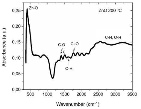
Fig. 5 shows the capacitance-voltage characteristics at10 kHz for the MIS capacitors. When a negative voltage is applied at the top contact, there is an accumulation layer of electrons in the ZnO film at the SOG/DI-ZnO interface, as are sult, the capacitance-voltage characteristics show the dielectric capacitance (Cox). On the other hand, when a positive voltage is applied at the top contact, the characteristics show a minimum capacitance due to the depletion region in the ZnO film at the SOG/DI-ZnO interface. From the capacitance-voltage characteristics, it can be observed that there is a very low hysteresis when the characteristics are forward and reverse measured. Nevertheless, at negative voltage values, the accumulation region presents effects of interface states (Neamen, 2003). Thisis attributed to the defects in the ZnO film near the dielectric-semiconductor interface, as the photoluminescence and FTIR spectroscopies show. Despite this, the MIS capacitors displaya similar behavior compared to the capacitance-voltage curvesin ZnO TFTs fabricated in silicon wafers with thermally grown silicon oxide as gate dielectric (Bang et al., 2011).

Fig. 5 Forward and reverse capacitance-voltage curves of the ZnO MIS capacitors using FTO and SOG/DI films as transparent electrode and dielectric,respectively.
Fig. 6. Current density of the ZnO MIS capacitors indicating the capacitor breakdown voltage at 36 V.Fig. 6 shows the current density of the ZnO MIS capacitors.Typically, in solution-processed devices, the evaporation of solvents during the deposition of the films induces pores and lower density in the film which affect the electrical characteristics ofthe devices (Yoo et al., 2013). The breakdown voltage of the MIS capacitor can be observed at 36 V because of the dielectric breakdown. Although a higher capacitor breakdown voltage was expected, the values of current density and capacitor breakdown voltage obtained are reliable for electronic devices applications (Park et al., 2013; Yoo et al., 2013).

Fig. 6 Current density of the ZnO MIS capacitors indicating the capacitor breakdown voltaje at 36 V.
From the overall characteristics presented, ZnO MIS capacitors can be explored to be used in transparent electronics. ZnO MIS capacitors were fabricated employing simple and low-cost solution-process techniques with no-vacuum needed, using feasible and easily-prepared precursor solutions.
4. Conclusions
In summary, the development of fully solution-processed zinc oxide metal-insulator-semiconductor capacitors employing the ultrasonic spray pyrolysis and spin-coating techniques was successfully presented. Fluorine tin oxide and spin-on glass were used as transparent electrode and dielectric film, respectively. The MIS capacitors were highly transparent, which their use makes feasible in transparent electronics. The capacitance-voltage characteristics showed a very low hysteresis when the characteristics were forward and reverse measured. The accumulation region presents effects of interface states attributed to the defects in the ZnO film near the dielectric-semiconductor interface, as the photoluminescence and FTIR spectroscopies showed.

