


 nueva página del texto (beta)
 Inglés (pdf)
 Artículo en XML
 Referencias del artículo
 Enviar artículo por email
 Citado por SciELO
  Similares en
SciELO
Similares en
SciELO 
 Permalink
1. Introduction
Cadmium sulfide (CdS) is a II-VI semiconductor material with an optical band gap of 2.42 eV and a great diversity of applications, such as window layers for both CdTe and CuInGaSe2(CIGS)-based solar cells devices (Elbar, Tobbeche, & Merazga,2015; Gerthoffer et al., 2015; Han et al., 2014; Lee et al., 2015;Li, & Liu, 2015; Mohamed, 2015; Yun, Cha, Ahn, Kwon, &Al-Ammar, 2014). The CdS/CdTe and CdS/CIGS heterojunction has been actively investigated as a photovoltaic junction, moreover, the CdS which acts as a window layer in the afore-mentioned solar cells has been deposited by many techniques such as sputtering (Kim, Kim, Choi, Park, & Lee, 2015), close space sublimation (CSS) (Cruz et al., 2013), chemical bath deposition (Yücel & Kahraman, 2015; Lisco et al., 2015), spraypyrolysis (Yilmaz, 2015), sol-gel, spin coating (Zhang, Huo, Li,Li, & Yang, 2013), thermal evaporation (Baghchesara, Yousefi,Cheraghizade, Jamali-Sheini, & Saáedi, 2016), ion beam sput-tering (Liang et al., 2013) and many others. The CSS technique consists in a source of an evaporating material and a substrate which are separated by small distance in a controlled atmosphere. It has the advantage of being an inexpensive deposition method because of its simple configuration and cheap materials (Cruz-Campa & Zubia, 2009), and it also has a high deposition rate (Alamri, 2003).
Glancing angle deposition is a novel and useful technique to grow nanostructured materials at low cost, which consists in tilting the substrate against the vapor flux. It is based on the oblique angle deposition (OAD) technique. In OAD the incident vapor flux arrives at non-normal angles (i.e., oblique angles) to a static substrate; therefore, the vapor flux can be treated as a vector, which has two components, a vertical and lateral component with respect to the substrate, which produces a distinct and directional columnar growth because of atomics hadowing mechanisms occurring at the substrate’s surface.At the initial stage of the deposition, adatoms condense ontothe substrate creating individual separated islands of deposited material, or nuclei (Kaiser, 2002). Tilting the substrate causes the incident vapor to arrive at oblique angles, which results in the appearing of shadowed regions where the vapor flux can-not directly reach the substrate. The nuclei capture the vapor flux that would have landed in the afore mentioned shadowed regions, leading to the formation of a columnar growth inthe same direction as the vapor source, resulting in the creation of a nano-array pattern. The glad technique differs with respect from the OAD in that the substrate is no longer static; instead, it is azimuthally rotated by a stepper motor. Controlling the rotation of the substrate and other deposition parameters, namely vapor flux incident angle, substrate temperature among others, it is possible to obtain three-dimensional nanostructures such as nano columns, zigzag, nanohelix, nanosprings and many others (Barranco, Borras, Gonzalez-Elipe, & Palmero, 2016; Jie, Yu, Qin & Zhengjun, 2008; Messier et al., 1997; Robbie & Brett, 1997; Zhou, Li, Ni & Zhang, 2011). The afore-mentioned nanostructures enhance the contact area for certain materials, which in turn changes their optical and structural properties; this could be beneficial for certain applications suchas optoelectronic and photocatalytic devices (Jie et al., 2008; Zhou et al., 2012). Furthermore, these structures could be integrated into a solar cell, which makes them very attractive fora wide variety of applications (Leem & Yu, 2011; Zhou et al.,2012).
In this paper, CdS thin films were prepared using the GLAD technique along with a sublimate vapor effusion source, which was under an azimuthal counter-rotation with respect to the sub-strate rotation direction, the effects of this deposition method onthe morphological, structural and optical properties of the films is reported.
2. Experimental details
Figure 1 shows the schematic representation of the evaporation source and the glass substrate in GLAD technique. Ω and ω are used to name the rotation velocity of the source and the substrate, respectively. The evaporation source consists of a graphite container axially rotated at Ω = 20 rpm and heated between two halogen lamps at 923 K. 2 g of a CdS powder (99.99% pure) were placed in the container. The pressure within the cavity was close to ∼7 × 10⁵ Pa. This was calculated assuming and ideal gas behavior (PV = nk B T), where V = 14.73 cm3 is the volume of the container, T (923 K) the evaporation temperature of the source, k B is the Boltzmann’s constant and n the numbers of moles. It must be clarified that although the ideal gas model might not betotally accurate to model the pressure of the container, it was made as a first approximation for the sake of simplicity, and for the immediate intents and purposes of this work it is considered sufficiently correct. The container has a top cover with 20 holes of ∼1.5 mm diameter symmetrically distributed as is shown in Figure 1(b); these holes have a vapor effusion function.The vapor flux density (Φ) for each hole was estimated using the cosine of Knudsen law (Herman & Sitter, 2012):

Fig. 1 Experimental setup for GLAD method combined with the sublimate vapor effusion source. The left side (a) shows the GLAD apparatus as it is implemented in the effusion source. Substrate and source movements are accomplished by two independent motors. On the bottom right (b), the source container is shown.
where a = 1.77 × 10⁻² cm2 is the area of a single hole, L = 6.0 cm is the distance between the substrate and the evaporation source, P G is the CdS vapor partial pressure with in the container, T(923 K) is the evaporation temperature of the source, M is the CdS molecular weight and α is the incident deposition flux angle.The flux density has an angular distribution in each hole; this produces a confined region of CdS vapor distributed between the substrate and the evaporation source.
To grow vertical nanocolumnar structures of CdS thinfilms, the substrate was put in GLAD mode, as shown inFigure 1(b), and heated by radiation using two halogen lampsas depicted in Figure 1(a). The substrate was azimuthally rotated using angular velocities with values ω = 20, 30, 40, 55,150, 350, 700 and 1020 rpm, and tilted using α = 0o, 20o and 80o, as shown in Figure 1(b). The experimental set-up procedure was as follows: Corning 2947 glasses and comercial ITO/Glass (Delta Technologies CB-40IN-0107) with dimensions of 25 mm × 25 mm × 0.7 mm were used as substrates, which were sequentially cleaned prior to the deposition by an ultrasonic agitation bath in distilled water, acetone and isopropyl alcohol for 5.0 min each. Subsequently, they were dried with N2 and heated at a substrate temperature (T s ) of 623 K.After reaching T s , a shutter placed above the evaporation source was removed, the substrate was put in front of it and adjusted in GLAD mode with a separation distance of L = 6.0 cm. Thesource and the substrate were put in counter rotation; this means that the source rotated in a direction opposite to that of the substrate. The background pressure in the vacuum chamber was ∼4 Pa and the deposition time was 1.0-3.0 min for different types of samples.
The cross-sectional morphologies of CdS films were characterized using a field emission scanning electron microscope (FESEM) JEOL 7600F instrument. The X-ray diffraction (XRD) data was obtained by a D5000Siemens X-ray diffractometer with a beam under of CuKα filtered monochromatic radiation (λ = 0.15418 nm) by 40 kV with 35 mA and aperture diaphragm of 0.2 mm. The diffractograms were registered in the step scan mode with a beam incidence angle of 1o and recorded in 2θ = 0.02o steps with a step time of 10 s in a 2θ range of 20-55o .The optical measurements were carried out using a UV-vis Agilent 8453 spectrophotometer with 0.1 nm resolution, in the rangeof 400-900 nm. The optical band gaps were calculated with direct transitions only.
3. Results and discussion
The flux density value defined by Eq. (1) decreases as α increases. Particularly, for α = 80o, Φ was estimated to be∼1 × 10²¹ CdS atoms/cm2s. At first glance, the films showed no evidence of pin-hole formation; this could be explained by the counter-rotation between the substrate and the evaporation source, which in turn could favor a uniform angular distribution of the CdS vapor flux.
The optimal ratio of ω/Ω was found to be 55/20, this value was selected from the optimization of the solar weighted transmission (SWT) calculation, while the other deposition parameters remained constant, this will be discussed in more detail later in the text.
After the growth of the CdS thin films, the transversal morphology was observed by FESEM with a magnification of 50,000 × and 100,000×. In order to obtain a SEM image with good quality, which would allow the correct visualization of the nanocolumnar structures, it was necessary to employ a deposition time of 3 and 2 min for the glass and ITO/glass substrate, respectively.
The cross-sectional image of the CdS arrays on glass substrates grown at α = 80o is shown in Figure 2(a). Highly uniformand densely packed arrays of CdS nanocolumnar structures were successfully formed; they displayed vertical alignments with great uniformity through all their thicknesses, which was of∼300 nm. The diameter of these structures was approximately 30 nm, and it was estimated from the zoom on the FESEM cross-section images. The presence of fissures with small gaps which divide some of these structures can also be observed.
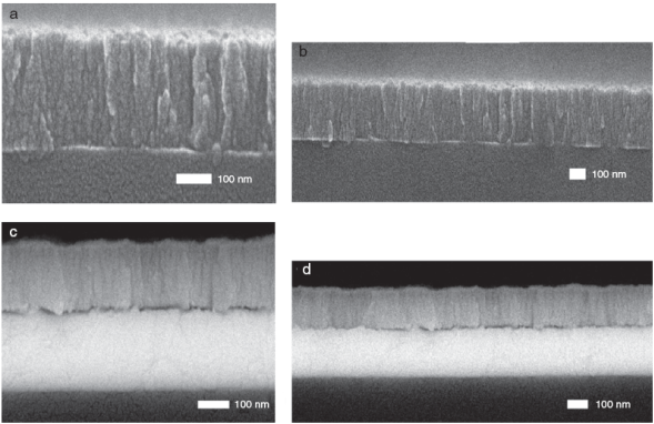
Fig. 2 FESEM image of: vertical nano columnar CdS as nanostructure grown at α = 80o on a glass substrate with a magnification of (a) 100,000× and (b) 50,000×. Vertical nano columnar CdS as nanostructure layer grown at α = 80o on an indium tin oxide (ITO)-coated glass substrate with (c) 100,000× and (d) 50,000×.
Figure 2(b) shows a transversal structure for the simple grown glass/ITO substrate at α = 80o. A uniform and dense columnar distribution was also observed, and the thickness ofthe thin film was approximately of ∼200 nm. However, the presence of fissures was less in comparison to the sample shown inFigure 2(a), since they were not present through all the thickness of the film. This was evidence that the CdS deposition was more densely packed on the glass/ITO substrate.
Figure 3 shows the XRD normalized pattern for the thin films grown at α = 0o, 20o and 80o with 1.0 min of deposition time. The single-phase hexagonal CdS Wurtzite structure (Razik, 1987) is observed with a preferential orientation in the (002) plane. Low intensity peaks for the (100), (101), (110), (103) and (112) planes are also observed. The XRD data showed that all the peaks are shifted toward higher 2θ values in comparison to that of the standard pattern (2θ = 26.507o); this is evidence of compressives train (Zak, Majid, Abrishami, & Yousefi, 2011). The crystal-lite size (DXRD) was calculated from the plane (002) using the Scherrer’s equation (Wang et al., 2015):
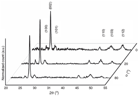
Fig. 3 XRD normalized pattern for CdS thin film grown with different incident deposition flux angles.
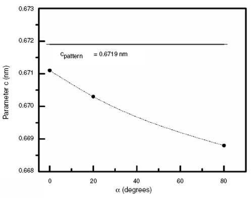
where β002 s the full-width at half-maximum and λ is the wave-length of the X-ray radiation employed (λ = 0.15418 nm). The values of DXRD are given in Table 1. The crystallite sizes values were between ∼25 nm and ∼35 nm. The lattice parameter c 002 was calculated employing the standard lattice geometry equations for the hexagonal structure (Iribarren, Hernández-Rodríguez, & Maqueira, 2014; Kaur, Kumar, Sathiaraj, &Thangaraj, 2013). As it was mentioned before, the shifting of the2θ positions to higher values with respect to the CdS standard pattern is evidence of a negative compressive strain, this suggests that the lattice parameters of the unit cell would show a decrease, this agrees with the reported c 002 lattice parameter values summarized in Table 1, which are in general smaller tan those of the standard CdS (c 0= 0.6719 nm).
Table 1 Structural parameters for samples with different incident deposition flux angles.
| α (degree) | 2θ002 (degree) | β002 (radians) ×10−3 | c 002 (nm) | ε (%) | D XRD (nm) |
| 0 | 26.54 | 4.6 | 0.6711 | −0.119 | ∼31 |
| 20 | 26.57 | 4.1 | 0.6705 | −0.208 | ∼35 |
| 80 | 26.63 | 5.7 | 0.6691 | −1.61 | ∼25 |
The c 002 parameter decreases for higher incident depositionflux angles, this correlation between the afore mentioned parameters is illustrated in Figure 4. The general reduction of the c 002 values indicates that there is shrinkage on the c-axis for the CdS unit cell with respect to the pattern value. Furthermore, the strain ε along the c-axis was calculated by using the expression ε = (c − c 0)/c 0× 100% (Ghosh, Basak, & Fujihara, 2004). The absolute values of the c-axis strain increase as α increases, this is also shown in Table 1. The negative values of ε confirm shrink-age in the c-axis. This suggests that a high incident deposition flux angle leads to a lattice compression effect along the c-axis direction, as it was also stated in the XRD analysis.
In order to find the optimal ω/Ω ratio the solar weighted transmission (SWT) was calculated for the thin films grown at different substrate rotation speeds (ω). Figure 5 shows the SWTas a function ω, for different samples all grown at α = 80o and with 1.0 min of deposition time. Based on the SEM images, this value of α was selected since it allowed observing with more clarity the nano-columnar deposition on the substrate. TheSWT formula is given by Mendez-Gamboa, Castro-Rodriguez,Perez-Quintana, Medina-Esquivel, and Martel-Arbelo (2016):
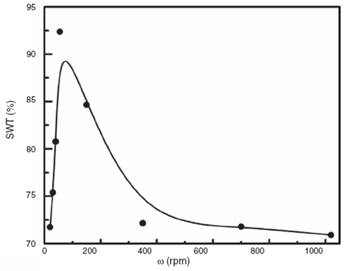
Fig. 5 Solar weighted transmission (SWT) measurements of CdS thin films asa function of substrate rotation grown with deposition flux angle of α = 80o.
where S(λ) is the AM 1.5 solar radiation spectrum, T(λ) is the optical transmittance, and the numerator of Eq. (3) represents the solar photon flux-weighted transmittance for the sample.The SWT is the ratio of the usable photons transmitted from the total available photons, it can be estimated through the normalization of the transmittance spectra, and this was done by integrating the solar spectral photon flux over the wavelength range of 400-900 nm. Figure 5 shows that SWT reached a maximum of ∼92% at ω = 55 rpm, and for greater ω it decreased to ∼71%. In accordance with the calculations of SWT a ratio ofω/Ω = 55/20 was selected as the optimum value.
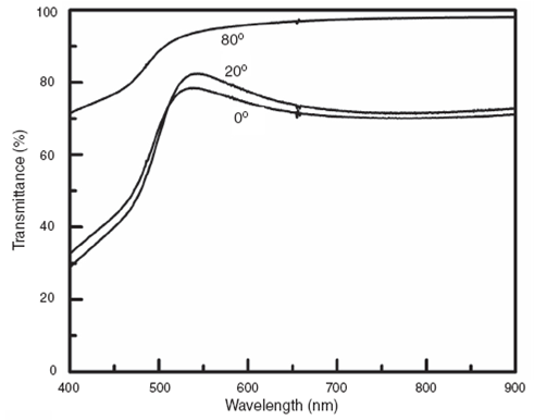
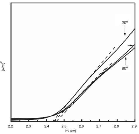
Figure 6 shows the transmittance spectrum of samples grown at α = 0o, 20o and 80o with 1.0 min deposition time. A transmittance value of ∼95% was observed for the sample with α = 80o.The increasing in the transmittance value is due to the changein the thickness, since a larger tilting angle leads to a smaller deposition rate (Nagiri, Yambem, Lin, Burn, & Meredith, 2015), resulting in thinner samples, which in turn will produce higher transmittance values. As can be seen, the transmittance for the film grown at α = 80o at the 400 nm wavelength is less tan 80%, while it is below 40% for the samples with α = 0o and 20o. The optical band-gap energy (E G ) was calculated using the Tauc formalism (Tauc, Grigorovici, Vancu, 1966) as shownin Figure 7, E G values between ∼2.43 eV and ∼2.45 eV were obtained, which agrees very well with the previous reports of theband gap energy for the CdS (Mohamed, 2015). Additionally, the refractive index (n) was calculated from the equation (Kim,Yim, Son, & Leem, 2012):
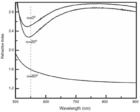
where R is the normal-incident light reflection, k is the extinction coefficient defined as k = α abs λ / 4π, where α abs is the absorption coefficient and λ the wavelength. In the region belowthe band gap energy the absorption follows A → 0.Then the expression T + R + A = 1 can be reduced to R = 1 − T from where it is possible to estimate the reflected light. The calculated refractive index at different incident deposition flux angles are depicted in Figure 8, which shows that it decreases as α increases. For α = 80o the refractive index was ∼1.6 at wavelength near 550 nm,for α = 0o and 20o it was ∼2.4, which is very close to the refractive index value that is required for a thin film that is desired to beused as an antireflection layer between ITO and CdTe accordingto the law (n ITO n CdTe )1/2 (Prevo, Hwang, & Velev, 2005) where n ITO and n CdTe are the refractive index of ITO and CdTe layers,respectively.
4. Conclusions
In this paper, an innovative source for vapor effusion isreported. Such a source was employed to provide a vapor flux inthe GLAD deposition mode which led to the obtaining of CdS vertical nanostructured thin films. The source and the substrate were counter-rotated with respect to each other, at an optimal ratio ω/Ω: 55/20. The effect caused on the morphological, structural and optical properties for the CdS thin films grown at different incident deposition flux angles was investigated. The principal characteristics of these CdS nanocolumnar thin films were a uniform distribution over the substrate with dimensions of height and diameters of ∼200 nm and ∼30 nm, respectively.The films showed a single hexagonal wurtzite structure phase with a preferential (002) plane orientation, band gap energy of ∼2.42 eV and a refractive index between ∼1.4 and ∼2.4 in wavelength of 550 nm.

