


 nueva página del texto (beta)
 Inglés (pdf)
 Artículo en XML
 Referencias del artículo
 Enviar artículo por email
 Citado por SciELO
  Similares en
SciELO
Similares en
SciELO 
 Permalink
1. Introduction
Nowadays, the use of electricity has increased and hence the demand increases a lot. Power generation by means of conventional sources, such as coal and oil, results in increasing the greenhouse effect and environmental pollution issues in the world. The shortage of energy generation and pollution issues has been a main obstacle for industrial growth. These issues make the researchers concentrate on the clean energy resources such as photo voltaic (Li, Haskew, Li, & Hu, 2011), wind (Kesraoui, Korichi, & Belkadi, 2011) and fuel cell. The generation of electricity from renewable sources is important to reduce global warming and energy demand in the future as their use does not produce pollution and also the resources área bundantly available in nature.
Among the renewable energy sources, the photovoltaic (PV) one is one of the most outstanding in the world, because it is reliable, ecofriendly, low-maintenance and because of it slow operational cost (Figueres, Garcerá, Sandia, Gonzalez-Espin, & Rubio, 2009; Li & Wolfs, 2008). PV-based standalone and grid-connected systems are fast developing power generation areas in recent days in all over the world. Generating power from PV is reduced because of partial shading and mis-match condition in town areas (Scarpa, Buso, & Spiazzi, 2009). Another disadvantage of PV systems is their low conversion efficiency with the current technology which makes the PV systemsan expensive technology. Because of these reasons, research work on this field has been carried out in recent years.
In the PV system maximum power point tracking algorithm sare used to increase the energy harvesting facility and to improvethe efficiency (Saravanan & Babu, 2016; Subudhi & Pradhan, 2013). The design of PV cells for study is considered with the rating of PMPP= 100 W and VMPP= 15 V. Also, to increase the performance of the system, high step up DC-DC converters are used to convert from low voltage to high voltage forrequired applications. The difficulties occurring regarding the DC-DC converter’s efficiency is due to the low input voltage, high in rush current and static gain. The boost converter is the conventional non-isolated step up DC-DC converter with limited static gain and high switching voltage stress were used in literature (Kjaer, Pedersen, & Blaabjerg, 2005; Li & He, 2011; Meneses, Blaabjerg, Garcia, & Cobos, 2013).
The conventional boost converter is used for high step up applications with high current ripples for power system which causes conduction losses. Most of the high step up converter is affected with high input current because of the inductance values (Al-Saffar & Ismail, 2015; Hsieh, Chen, Liang, & Yang, 2013; Kim & Moon, 2015; Saravanan & Babu, 2015). To reducethat, the switching frequency has to be increased and hence it reduces the voltage stress occurring in the switches (Fardoun &Ismail, 2010; Wai, Lin, Duan, & Chang, 2007). Moreover, soft-switching is needed to reduce the switching loss and to improvethe performance.
Various researchers use the SEPIC converter (Chiang, Shieh, & Chen, 2009; Kim, Choi, Jang, Lee, & Won, 2005; Park, Moon,& Youn, 2010; Pazhampilly, Saravanan, & Babu, 2015) and the modified SEPIC converter (Park, Seong, Kim, Moon, & Youn,2008; Song, Oh, & Kang, 2012) for high static gain applications. The modified SEPIC converter has twice the static gain (De Melo, Gules, Romaneli, & Annunziato, 2010) value when compared with the conventional boost converter and also the switching voltage is half of the output voltage is value occurred (Yang, Liang, & Chen, 2009). In this paper, a converter with high static gain with reduced switching stress is proposed based on the SEPIC converter design. Compared with other converters, the proposed method gives reduced input in rush current for inductor, with faster settling time and less peak time of output voltage.
This paper is organized as follows: Section 2 describes the DC-DC converters operation and compares the boost and SEPIC with its merits and demerits. Section 3 presents the design of the proposed converter and its operation along with the chosen parameters. In Section 4 the analysis and results for the various DC-DC converters along with the proposed converter are explained briefly. The paper concludes the performance merits of the proposed converter in Section 5.
2. DC-DC converter
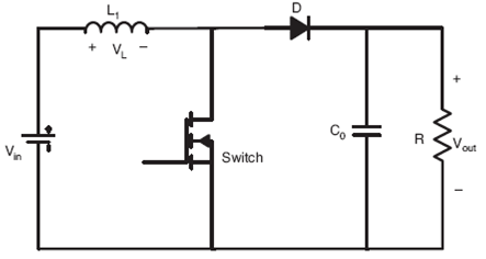
The converter is used to convert variable dc voltage to the fixed dc voltage for many DC applications. The main advantage of the high step up DC converter is the generation of the high voltage, i.e., from the input it is possible to generate ten times greater output using a single power semiconductor switch. The boost converter is a conventional high step up converter used inhigh voltage applications. The boost converter is based on the step up principle used for output voltage which is greater than the input voltage and its circuit model (Gules, Dos Santos, Dos Reis, Romaneli, & Badin, 2014; Park & Kim, 2012; Santos, Antunes, Chehab, & Cruz, 2006), as shown in Fig. 1. To improve the efficiency of the boost converter it is connected with both coupled inductor and switched capacitor (Li & He, 2011). During highstep up operation, current ripple is larger in the power devices and causes conduction loss which turns off the current.
For high voltage application, the switching voltage is almost equal to the output voltage of the converter. To improve the efficiency of the boost converter, it is upgraded to the conventional interleaved boost converter (Nejabatkhah, Danyali, Hosseini, Sabahi, & Niapour, 2012; Lee, Lee, Cheng, & Liu, 2000; Huanget al., 2004; Yao, Chen, & He, 2007). It consists of two switches to reduce the current ripple but a reverse recovery problem occursin the diode.
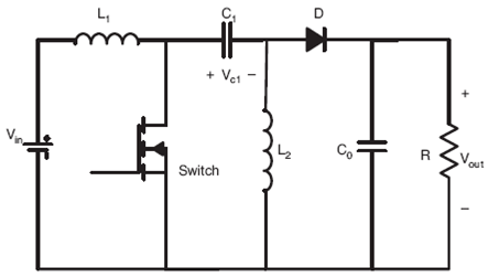
The single-ended primary inductor converter (SEPIC) follows both the step-up and step-down principles. It consists of two inductors for buck or boost operation of the input voltage for output with no polarity reversal, as shown in Fig. 2. It transfers energy through capacitor C1 and inductor L1; because of that, the switching voltage is higher than the boost converter. The static gain of the converter used for wide input voltage application. The voltage flow in the switch is almost equal to the sum of both input and output voltages. The in rush input current is low when compared to the boost converter but the voltage stress is high.
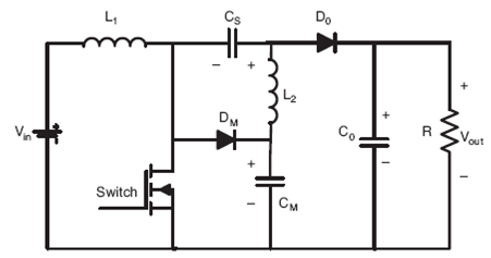
The conventional SEPIC converter is modified using diode DM and capacitor CM is (Gules et al., 2014) added in the converter circuit as in Fig. 3. It is the combination of the SEPIC and boost converter which improves the static gain. The static gain is enhanced by charging the CM capacitor using the conventional boost converter’s output voltage. The static gain is doubled and the switching voltage is reduced to half of the value than that of the boost converter. In this, high startup inrush current flows through the inductor L1, and to reduce that, a large input inductor is required. It consists of soft switching operation for turnON and turn OFF condition for all low input voltages.
3. Proposed converter
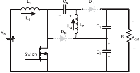
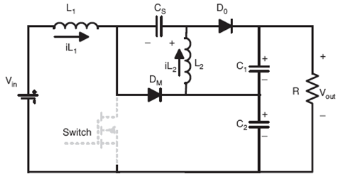
The proposed converter is shown in Fig. 4, with modification on the SEPIC converter to improve the performance and to reduce the in rush current of inductor. It also works in the combination of both boost and SEPIC mode but the connection of output capacitor is slightly modified. The proposed converter reduces the in rush current for inductor L1 and improves the operation of the converter faster than other converters.
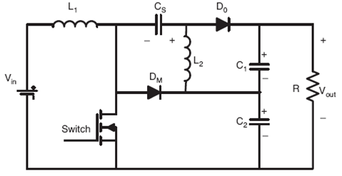
It also reduces the stress and utilizes the low voltage for switching in the converter for high voltage conversion. It consists of one switch S, two inductors L1 and L2, two diodes D0 and DM, and three capacitors C1, C2 and CS. The sum of the C1 and C2 capacitor’s voltages is equal to the output voltage of the converter.
When the switch is on, the diode D0 and DM are reversed biased and the charges are stored in inductors L1 and L2, as shown in Fig. 5. The input voltage flows through inductor L1 to the inductor L2 through Cs and C2. The capacitor voltage VC2 is equal to the switching voltage.
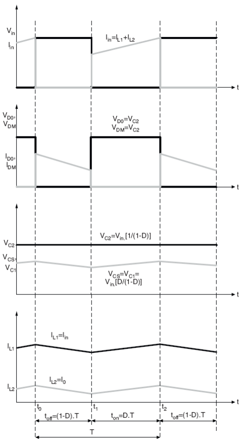
When the switch is off, the diode D0 and DM are in forward biased condition and stored energy from inductor L1 starts discharging, as shown in Fig. 6. The output flows through CS and C2 and inductor L2 discharges the energy through diode D0. The switch voltage is almost equal to capacitor voltage C2. The main theoretical waveforms of the proposed converter are presented in Fig. 7.
The voltage across the switch and all diodes are equal to the capacitor C2 voltage. The output voltage is equal to the sum of the capacitor voltage C1 and C2. The performances of the conventional boost, SEPIC and modified SEPIC were presented in this paper as the proposed converter is obtained from the design modification of these converters. The equation was derived for the proposed converter to calculate the inductance and capacitance using the conventional design.
The static gain of the proposed converter depends on the average inductance voltage with zero steady state. The duty cycle relation is presented in (1) considering continuous conduction mode operation. Duty cycle relation of the proposed converter is a combination of both boost and SEPIC converters. The output voltage of the converter is greater than that of the conventional boost and SEPIC converter.
The capacitor C2 voltage V C2 is calculated by (2) and is equal to the output voltage of the conventional boost converter. Thes witching voltage of the proposed converter was the same as the C2 capacitor’s voltage. During the off condition of the switch the diodes D0 and DM were in conduction mode and the relation was obtained as (3),
The voltage across the series capacitor, V CS and C1 capacitor voltage, VC1 was calculated by (4),
The design considerations for the proposed converter, and for other ones, were obtained by assuming the following ratings (Gules et al., 2014):
Input voltage = 15 V,
Output voltage = 150 V,
Output power = 100 W,
Switching frequency = 24 kHz.
The inductances L1 and L2 were designed using the stated expression in Table I by assuming the current ripple (△i L) as5A. The average current rate in inductor L1 was equal to the input current and the average current rate in inductor L2 is equal to the output current of the converter.
For the design of output capacitors C1 and C2, the output voltage ripple (△V out) was chosen as 1% of the capacitors’ voltage. The series capacitor CS was calculated using the nominal capacitor voltage ripple (△V C) equal to 10%. A small capacitance value was obtained and a low series equivalent resistance was used for the capacitors (Kim & Moon, 2015).
The selection of the semiconductor switch rating was done based on the sum of the current flowing rate in L1 and L2.Fig. 7 shows that the switching current starts flowing through thes witch during the turn-on period. The rating of diode in the proposed converter is chosen based on assumption, that the average current of diode is equal to the output current (I out). The total conduction loss of switch and both diodes are equal to the 2 W.The design expression utilized to design the boost, SEPIC (Hart, 2011), modified SEPIC and proposed converter parameters as shown in Table 1. The theoretical values estimated and the parameter values of the converter chosen are displayed in Table 2. These parameters were used to obtain the suitable output for the step up conversion in the converters with more reliability.
Table 1 Converters formulas.
| Parameters | Boost converter (Hart, 2011) | SEPIC (Hart, 2011) | Modified SEPIC (Melo et al., 2010; Gules et al., 2014) | Proposed converter |
| Switch Duty Cycle |
|
|
|
|
| Inductance |
|
|
|
|
|
|
||||
| Capacitors |
|
|
|
|
|
|
|
|||
|
|
|
|
aNominal capacitor voltage ripple
Table 2 Converters parameters.
| Parameters/Components | Boost converter | SEPIC | Modified SEPIC | Proposed converter |
| Input voltage (V in) | 15 V | 15 V | 15 V | 15 V |
| Switching frequency (f) | 24 kHz | 24 kHz | 24 kHz | 24 kHz |
| Duty cycle (D) | 0.9 | 0.91 | 0.82 | 0.82 |
| L1 | 112.5 μH | 113.75 μH | 102 μH | 102 μH |
| L2 | - | 113.75 μH | 102 μH | 102 μH |
| C1 | - | 1.518 μF | - | 50 μF |
| C2 | - | - | - | 50 μF |
| C0 | 100 μF | 100 μF | 100 μF | - |
| CS | - | - | 3.37 μF | 3.37 μF |
| CM | - | - | 3.37 μF | - |
| R | 224.88 Ω | 224.88 Ω | 224.88 Ω | 224.88Ω |
4. Results and discussion
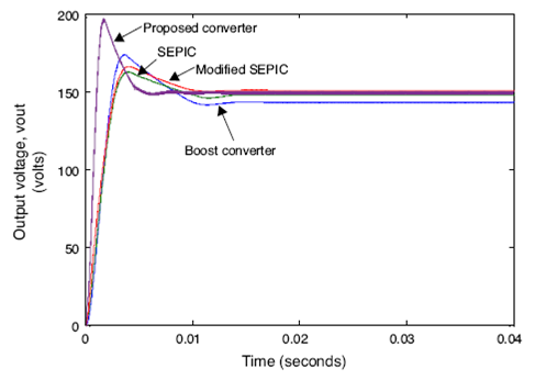
The proposed converter and other converters shown in Figs. 1-4 have been simulated using MATLAB/Simulink tocheck the above design parameters as well as to measure their performance and operations. The output voltages of the boost, SEPIC, modified SEPIC and proposed converter are shown in Fig. 8. From Fig. 8, it is observed that the output voltage of the proposed converter (150 V) increases 4.5% in comparison to that of the boost converter (143.3 V). The performances of the converters stability were verified by varying the duty cycle given to the switches and the output voltage of each converter was noted down. Based on that varying condition, the performance of the proposed converter was validated as discussed below.
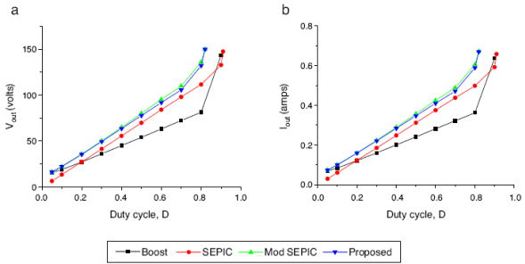
The output voltage and output currents of each converter with respect to various duty cycle were plotted in the graph as shown in Fig. 9(a) and (b). From the graph, it is easily observed thatthe proposed converter and modified SEPIC converter generate the output voltage and current as per the design of converter. But the boost and SEPIC converter gave reduced voltage and current. Also, the duty cycle designed for the boost and SEPIC converters was higher than the proposed converters.
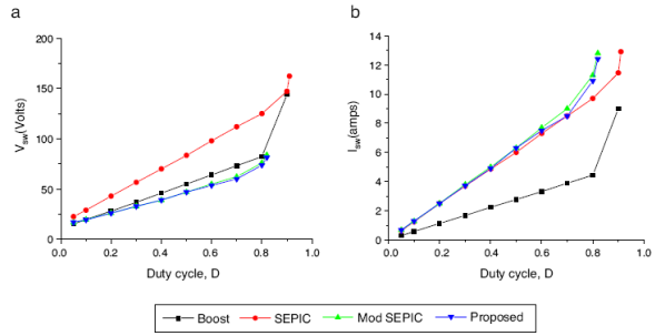
The switching voltage and current of the modeled converters were shown in Fig. 10. The switching voltage of the proposed converter was slightly lower than that of the modified SEPIC converter where as the switching voltage was high in the SEPIC and boost converter. Because of this lower switching voltage, the losses also decreased and the converter worked more efficiently in the high step up operation.
The input current and input peak current values are plotted in Fig. 11. When the input current flows through inductor L1, thecurrent ripple increases. This reduces the overall efficiency ofthe converter and also makes the converter to require high rating components. The proposed converter shows low input current ripple compared to the boost, SEPIC and modified SEPIC converters. In addition, the peak current of the proposed converter is comparatively lower than that of the other converters. The comparative results of the measured parameters of the proposed and compared converters are listed in Table 3.
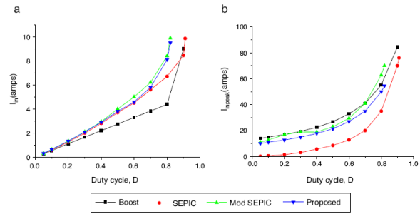
Table 3 Performance measured of proposed and other converters.
| Parameters/Components | Boost converter | SEPIC | Modified SEPIC | Proposed converter |
| Output voltage (V out) | 143.3 V | 147.5 V | 150 V | 150 V |
| Switch voltage (V s) | 144.1 V | 162.3 V | 83.8 V | 81.3 V |
| Inductor starting current (I in) | 84.5 A | 76 A | 70 A | 54.5 A |
| Output current (I out) | 0.6372 A | 0.6577 A | 0.6715 A | 0.6699 A |
| Output power (Pout) | 91.31 W | 97 W | 100 W | 100 W |
The time responses of the output voltage for the converters were analyzed and the settling time and peak time of the output voltage are plotted in Fig. 12(a) and (b). From the analysis, it is clear that the proposed converter operates with fast settling and less peak time compared to other converters; because of that, the converter gives a quicker response for the required application.
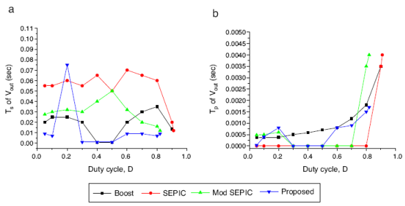
Similarly, the time response characteristics of the input current were analyzed and are shown in Fig. 13(a) and (b). As the peak time of the proposed converter decreased, the in rush current magnitude also decreased with a quicker response. These analyses show the advantages and the performance improvement of the proposed converter when compared with the other analyzed converter models. Even though the proposed converter has several advantages compared with other converters, it requires more complex technology.
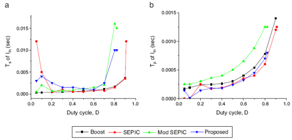
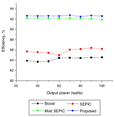
Fig. 14 shows the obtained efficiency of the various converters along with the proposed one. The graph clearly shows that the proposed converter has more efficiency than the other ones. The proposed converter operates a fast response with low input current for the system. The proposed converter efficiency is equal to 92.5% at full load condition for 100 W where as for the same condition, the boost, SEPIC and modified SEPIC converters achieve 84.2%, 86.4% and 91.7%, respectively.
5. Conclusion
A high step up non-isolated DC-DC converter is presented in this paper. The proposed converter uses two loading capacitors with equal rating instead of one capacitor in the SEPIC model.These capacitors share the voltage stress and the in rush current.Furthermore, the time response characteristics of the output load voltage improve by reducing the settling and peak times. The performance of the proposed converter model is analyzed undervarious parameters. The efficiency of the proposed converter is equal to 92.5% with an input voltage of 15 V, an output voltaje of 150 V and an output power of 100 W. The proposed converter analysis shows that it has a reduced switching voltage of 81.3 Vand reduced starting current of 54.5A. The time response analysis of the proposed converter shows that the output current and voltage characteristics settle to the steady state value quicker in 9 ms. Also, the peak time of the voltage and current of the proposed converter is 1.7 ms.
The validation of the proposed converter concludes that its performance is better than the one of the compared converter models and that it can be a good choice for many of the renewable energy system applications with simple design and high efficiency.

