


 nueva página del texto (beta)
 Inglés (pdf)
 Artículo en XML
 Referencias del artículo
 Enviar artículo por email
 Citado por SciELO
  Similares en
SciELO
Similares en
SciELO 
 Permalink
1. Introduction
The mainstay of any digital system, interacting with real world, is the data acquisition of the signals from various systems. The requirement for data acquisition is to quantify an electrical or physical phenomenon such as voltage, current, temperature, pressure or sound. Though every data acquisition system (DAS) is defined by its application requirements, every system shares a common goal of acquiring, analyzing, and presenting information. DASs blend signals, sensors, actuators, signal conditioning, data acquisition devices and application software (Abdallah & Elkeelany, 2009; Marino, Poza, Otero, & Dominguez, 2010). Data acquisition involves amassing analog signals from measurement sources and digitizing the signal for storage, analysis, and presentation or control. Generally, sensors provide continuous data about a particular aspect of a process such as voltage, current, temperature and so forth in an analog form which needs to be converted into digital form and also need further processing after acquisition. Consequently, analog signal is converted into digital through analog to digital converter (ADC). The obtained data may now be transmitted on a digital bus to the central processing unit for further analysis. Digital transmission is more immune to noise than analog data from the sensors (Abdallah, Elkeelany, & Alouani, 2011; Siddiqui, Grosvenor, & Prickett, 2015).
Existing DAS are bulky, expensive and/or require design redundancy to attain high reliability and high speed acquisition. Therefore, embedded processors must be used to reduce system size, evade design redundancy, lessen cost and power consumption. Field Programmable Gate Array (FPGA) is one such innovation in embedded systems arena which is more expedient due to high degree of parallelism, low power consumption, input and output (I/O) capabilities. Its computational throughput can be higher than typical digital signal processors (DSPs) at a much reduced cost because hardware resources of FPGA can be configured to adapt to the demands of specific application (Monmasson et al., 2011).
In general, DAS can acquire single channel or multi-channel signals. An instinctive usage of multi-channel A/D conversion is to use a dedicated ADC for each channel or to use a single ADC with time division multiplexing. Most of the ADCs use time division multiplex, wherein the number of channels is less. Majority of FPGA boards have lesser number of ADC channels which constrains them to intake large number of external analog signals, subsequently their function as controllers in DAS.
Further, proper communication between the devices plays a crucial role in establishing automation in any system. Communication through global system for mobile communication (GSM) is rapidly growing albeit being completely dependent on the service provider thus making it prone to network failures very often whereas communication through Ethernet is an independent network and highly reliable. There exists a wide range of network protocols available in the market and according to the application, a suitable protocol can be chosen and utilized in establishing reliable communication and data transfer (Anish, Kowshick, & Moorthi, 2013; Fischmeister, Trausmuth, & Lee, 2009; Uchida, Fujii, Nagasaka, & Tanaka, 2006). Taking the importance of communication and monitoring after data acquisition into consideration, it is vital to combine data acquisition, monitoring and communication and design a universal platform such that it is universally flexible for any sort of system. To this end, this paper proposes a method for FPGA boards with lesser number of onboard ADC channels to intake higher number of signals thereby extending their functionalities in DAS. Further, an embedded platform is proposed which integrates data acquisition, monitoring and allows communication between the FPGA boards in a network. Ethernet interface has been used for one to one communication between FPGA boards where one acts as server and other as client. The status of the appliances connected to the client are passed onto the server for monitoring. This enables easy supervisory and control of appliances situated in remote location. The developed platform is tested with Altium Nanoboard (NB3000) FPGA board which has a four channel onboard ADC and XILINX SPARTAN 3AN FPGA. The onboard FPGA chip has TSK3000A (32-bit soft-core) processor inside it. The proposed embedded platform utilizes both hard core digital components and softcore processor available inside single FPGA for data acquisition, monitoring and communication. This FPGA along with softcore processor has several advantages over standard microcontroller because of their features such as high flexibility, fast computation, less design time to market with moderate cost and most importantly the hardware holds the feature of dynamic reconfiguration. Also, the softcore processors provide access beyond the FPGA chip through integrated standards or custom-made interfaces such as Ethernet, graphical user interface (GUI), etc. (Joost & Salomon, 2005). In the proposed work, hard core digital components programmed with very high scale integrated circuits (VHSIC) hardware descriptive language (VHDL) has been used for data acquisition. Softcore processor programmed with embedded C has been used for monitoring the data and Ethernet communication.
2. Proposed embedded platform
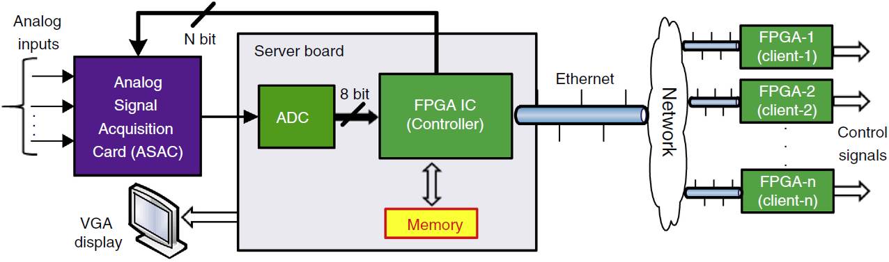
The block diagram of the proposed embedded platform is shown in Figure 1 which acquires the data, monitors the data and provides one to one communication between the FPGA boards connected in a network through Ethernet interface. The proposed platform is divided into three parts. (A) Data acquisition, (B) Monitoring and (C) Ethernet communication, which are discussed below.
2.1. Data acquisition
In order to enhance the functionalities of the FPGA boards with lesser number of onboard ADC channels in DAS, a scheme has been proposed in which an analog signal acquisition card (ASAC) is connected to FPGA board thereby enhancing the external analog signal accessibility of the board. ASAC is an integration of analog multiplexer with each channel of onboard ADC of host FPGA board in which the value of selection bits (Y) for analog multiplexer is furnished and controlled from the embedded block developed inside FPGA. A counter is devised inside FPGA, which provides selection bits for analog multiplexer through I/O pins of host FPGA board.
The conceptual design of proposed system is illustrated in Figure 2 in which ASAC is integrated with the host FPGA board. In this figure, 2 N (or less) analog input signals are connected to an analog multiplexer which in turn select one of them depending on N-bit combination of selection lines. The output of each multiplexer is given to one particular channel of onboard ADC and multiplexer controller is embedded inside FPGA as well.
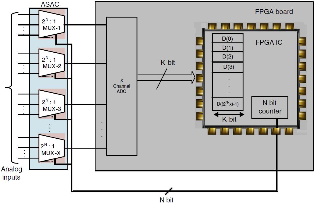
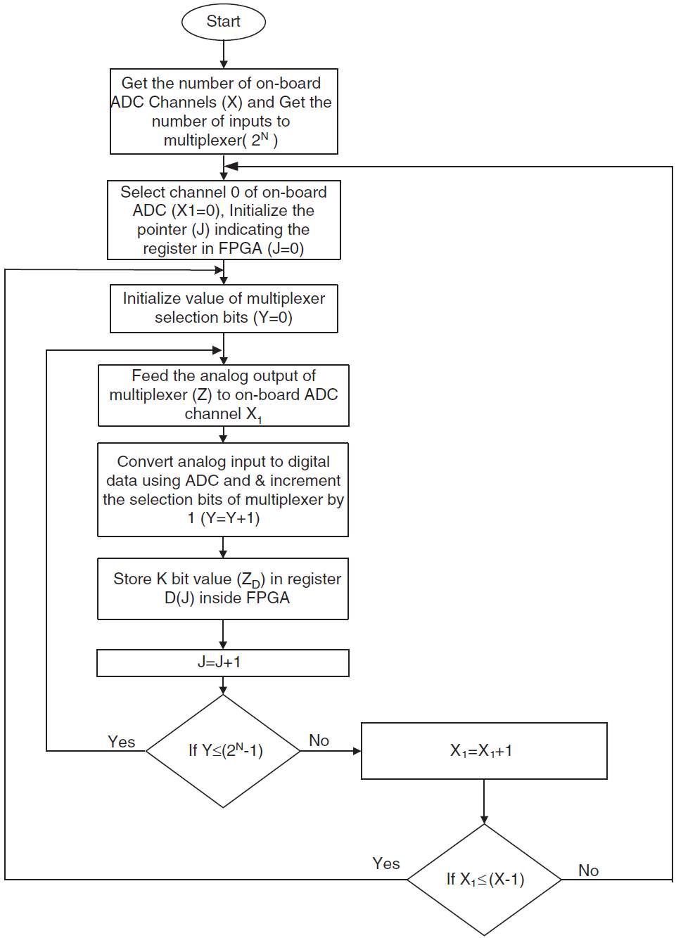
A generalized flowchart of the algorithm implemented in FPGA is shown in Figure 3. For instance, a host FPGA board with X number of ADC channels may be considered. By including a 2 N : 1 multiplexer in each channel, the number of channels accessed by FPGA increases to 2 N *X. Let X 1 be the present channel accessed by the FPGA (if X = 4, then X 1 = 0, 1, 2, 3). As a first measure, X 1 and the selection bits given to multiplexer are set to zero. Presently, the analog signal corresponding to the first input of first multiplexer is read through ADC during its acquisition time. The counter meant for selection bits is incremented by one during the conversion time of ADC. Thus providing ample amount of settling time for the analog input to settle at its output. The value of the counter is made to zero, once 2 N channels of the present multiplexer are read by FPGA. Then the next ADC channel is selected (X 1 = X 1 + 1). Once X 1 reaches its maximum value (X), it is reset and the process is rehashed for continuously reading the signals.
The maximum sampling frequency that embedded platform can achieve depends upon the maximum sampling frequency of the ADC and also on the number channels to which it has to be enhanced. For e.g. if Z is the maximum sampling frequency of the ADC and N is the number of channels to which it has to be enhanced, then the sampling frequency of system that can be achieved is (Z/N).
2.2. Monitoring
The hardware requirements for displaying the information on VGA monitor from FPGA board include a soft-core processor inside FPGA (TSK 3000A - 32 bit RISC processor), VGA controller and SRAM controller. The TSK3000A processor executes the native software code to boot up the FPGA board and initialization of other software wrappers apart from executing user written software code. The VGA controller provides the interface between the hardware controller elements on the FPGA board and the software wrappers to bring up and initialize the VGA monitor. The SRAM controller provides memory for the display operations in terms of data buffers where the data is stored before it is sent to the VGA monitor.
The flowchart for the software code, which runs for the display of information on VGA monitor, is shown in Figure 4. The graphics t structure (inbuilt) initializes the display driver on the FPGA board further it activates all hardware components and runs all associated software wrappers, which deal with initializing the display drivers on the FPGA board and the VGA monitor. The canvas t structure (inbuilt) helps the user in initializing in a way it has to be displayed in the monitor. Once the graphics driver and canvas are initialized, the canvas is filled with any background color and is set to visible. Thereafter, information is passed onto the monitor for display in terms of a string, x and y coordinates of position of display, text color and styles. Since the developed display system is an online monitoring system, the program runs individually for all the data that has to be monitored. Whenever there is a change in the monitoring data such as change in measured parameters, the display is updated after erasing the existing data.

2.3. Ethernet communication
Ethernet is a common name given to various closely related network standards. Many systems employ TCP/IP suite as it offers reliable, ordered, and error-checked delivery of the stream of packets between the devices running over an Internet Protocol (IP) network. In TCP/IP suite, Transmission Control Protocol (TCP) is responsible for breaking down data into small packets before they can be sent over a network at the sending end, and for assembling the packets again when they arrive at the receiving end. IP takes care of the communication between devices and it is responsible for addressing, sending and receiving the data packets over the internet.
The TCP/IP protocol is designed such that each computer or device in a network has a unique IP address and each IP address can open and communicate over up to 65,535 different ports for sending and receiving data between any other network device. The IP address uniquely identifies the device on the network and port number indicates a specific connection between one device and another (i.e. between two IP addresses). A TCP/IP port can be thought of as a private two-way communications line where the port number is used to identify a unique connection between two devices.
Once the IP address is assigned for each FPGA device and port number for communication between the FPGA devices, a client/server model is used. In client/server mode, a TCP/IP client initiates communication with the TCP/IP server by sending a request packet. When the server receives the request, it processes it and responds. Once connection through a TCP/IP port has been established between client and server, data can be sent in either direction and is open until either the client or the server terminates the connection. One extremely good benefit of the client/server TCP/IP protocol is that the low level drivers that implement the sending and receiving of data perform error checking on all data and it is guaranteed that there will be no errors in any data sent or received.
In the present scheme, TCP/IP suite has been used for establishing Ethernet communication between two FPGA boards in which one acts as a master/server and other as slave/client. The server controls the client by sending the switching commands for the operation of appliances which are connected to the client. The client then processes the commands received and translates them into actions of switching particular appliances ON or OFF. This type of control system gives the liberty for control of appliances from remote locations connected through Ethernet. Further, the status of appliances are displayed at server end for monitoring.
Implementation of the Ethernet communication on Altium Nanoboard involves peripherals such as Random Access Memory (RAM), Ethernet port, Serial Peripheral Interface (SPI) master controller and I/O port which are interfaced with TSK3000A processor. The TSK3000A is a Reduced Instruction Set Computing (RISC) processor compatible with the Wishbone bus system. The Ethernet family of peripheral devices provide an interface between a processor and a physical layer device through the provision of the IEEE802.3 Media Independent Interface (MII). Communication with multiple slave SPI peripherals are controlled by the SPI master controller. The I/O port block is a Wishbone-compliant, configurable parallel port unit, offering a simple register interface for storing data to be transferred to/from other devices in a design.
3. Test case
To test the functionality of the proposed embedded platform in real time application, a prototype of standalone micro-grid has been built in the laboratory which is elaborated in this section.
3.1. Micro-grid
Micro-grid system is a small-scale power system consisting of distributed renewable energy sources and loads (Park & Candelaria, 2013; Venkatraman et al., 2016). Due to the distributed nature of the micro-grid approach, the connection to the central dispatch utility can be removed or minimized so that the power quality to sensitive loads can be enhanced. Generally, micro-grid has two modes of operation: stand-alone (islanded) mode and grid-connected mode. Further, micro-grid systems can be divided into AC bus and DC bus systems based on the bus to which the component systems are connected (Chen, Wu, Song, & Chen, 2013; Di Silvestre, Graditi, & Sanseverino, 2014; Natsheh, Natsheh, & Albarbar, 2013).
A stand-alone micro-grid is formed by integrating multiple types of renewable energy sources, namely, wind and solar along with diesel generator (DG) as well as energy storage system. The overall schematic is shown in Figure 5 and the hardware setup for the same is shown in Figure 6. A DC bus is formed using wind energy conversion system (WECS), battery bank and PV array with DC-DC converter. A diesel generator is connected in parallel with the output of inverter. Furthermore, loads are classified as critical load (CL) and non-critical load (NCL) depending on the priority assigned for shedding the loads.


Since the monitoring places of resources (sources and loads) are widely distributed geographically, two FPGA controllers, source FPGA controller and load FPGA controller have been used which are connected through an Ethernet interface employing TCP/IP suite.
In micro-grid implementation and controlling, the source controller has to entree photo voltaic array voltage and current (V PV and I PV), wind generator voltage and current (V W and I W), battery voltage and current (V B and I B), three-phase AC load voltage and current (v lr, v ly, v lb and i lr, i ly, i lb) and three-phase AC diesel generator voltage and current (v dr, v dy, v db and i dr, i dy, i db). Consequently, a total of 18 signals have to be given to the source controller. The load and DG voltages are balanced, so reading any one of the three-phase voltages is sufficient for calculating the power. Thus, the number of analog signals fed to source controller reduces to 14. The host FPGA board has only four ADC channels. Therefore, a 4:1 multiplexer has been added to each channel of the onboard ADC of the source controller. By implementing the DAS proposed in Section 2, a total of sixteen input lines will be available. The 14 signals required for controlling and monitoring the micro-grid are fed to the source FPGA using the enhanced sixteen input lines.
The source FPGA controller after acquiring the voltage and current signals from various energy sources and loads, computes the generated and load power respectively. Based on the power imbalances between the generation and demand, the source controller decides upon switching ON/OFF the non-critical loads and the decision is communicated to the load FPGA controller through Ethernet interface.
The load FPGA controller controls different non-critical loads as per the command given by the source controller in accordance with the priority assigned to the loads. Based on the control activity provided by the load controller and the available power, the source controller disconnects the DG by activating/de-activating the relevant contactor. The electrical quantities, the status of the sources and the loads are displayed using a monitoring system for visualization. An algorithm has been developed to realize the above logic of the controllers and the flow chart of the developed source and the load control algorithm is presented in Figure 7.

As per the flowchart, the control logic can be summarized as follows:
Initial State:
Diesel Generator (PDG) : OFF and
All loads are ON
The power calculations are carried out as follows:
The logic of load control:
If PL > PG ⇒ SWITCH OFF NCL2
If still PL > PG ⇒ SWITCH OFF NCL1
The generated power and battery will supply the CL alone. If P G increases, and if
PG > PL ⇒ Switch ON NCL1
Still, if PG > PL ⇒ Switch ON NCL2
The logic of source control:
If PG < PL and both NCL1, NCL2 are OFF and
If
The steps involved in the Ethernet communication between the controllers are shown in Figure 8(a) and (b). The communication algorithm that runs in the source controller starts with the initialization of related Application Programming Interface (API), creation of a socket and binding to it. This step is followed by accepting the connection from the load controller. The statuses of the sources (amount of power generated, ON/OFF condition) are sensed, digitized using ADC, updated and displayed on the display unit. The control packet based on the status is sent to the load controller. Based on the control packet information, the load controller will switch ON/OFF the non-critical loads as per priority to equal the total power generated with the load power. Similarly, based on the packet received from the load controller, the control signals will be sent by the source controller to switch ON/OFF the DG to match the total power generated with the load power. The status information will be updated time to time (periodically) in the display unit connected with the source controller. The act of source and load controllers will be in such a way that source controller will act as a master/server and the load controller as a slave/client. Figure 9 presents a photograph of the display of micro-grid monitoring system wherein the values of all parameters are displayed which ascertains the efficient functioning of the proposed embedded platform.

Fig. 8 (a) Flowchart of program running in source FPGA controller. (b) Flowchart of program running in load FPGA controller.

4. Conclusion
A comprehensive embedded platform for data acquisition, monitoring and communication between the FPGA boards has been proposed. Further, a method to enhance the functionality of the FPGA boards with lesser number of channels in data acquisition system is proposed. The developed platform successfully utilizes server/client architecture mode for Ethernet communication between the FPGAs in which the control signals for the appliances connected to the client are controlled by the server and the status of appliances are displayed at server end for online monitoring. Data acquisition has been programmed using VHDL and for graphical interface and Ethernet communication embedded C has been used. The proposed embedded platform also works without a dedicated personal computer. The real time capability of the embedded platform is validated through the prototype of micro-grid developed in the laboratory.

