


 nova página do texto(beta)
 Inglês (pdf)
 Artigo em XML
 Referências do artigo
 Enviar este artigo por email
 Citado por SciELO
  Similares em
SciELO
Similares em
SciELO 
 Permalink
1. Introduction
The rapid expansion and revolution of wireless technology has drawn new demands for integrated components including antennas. Antenna is one of the main components of the integrated low-profile wireless communication systems; therefore, antennas miniaturization is necessary to achieve the optimal design. Some wireless applications of antennas are desired to operate simultaneously for Wireless LAN, Worldwide Interoperability for Microwave Access (WiMAX) and some next generation wireless technologies.
The basic geometry and configuration of the U-slot antenna was introduced in 1995 by Huynh and Lee as a single-layer, single-patch wideband linearly polarized microstrip patch antenna. Multiband antennas (Lee, Luk, Mak, & Yang, 2011) can cover multiple wireless technologies; however, in microstrip patch antennas, the U-slot was mainly used for bandwidth enhancement rather than introducing a band notch and it has been shown that the U-slot technique can be used to design patch antennas with dual and multi-band characteristics. The studies reported (Lee, Steven Yang, Kishk, & Luk, 2010; Singh, Ali, Singh, & Ayub, 2013) on U-slot patch antenna showed that, it can be intended not only for wideband applications, but also for multiband (dual and triple-band) applications. It is even more complex to integrate multiple bands for wireless technologies (Vedaprabhu & Vinoy, 2010) such as AWS (Advanced Wireless Services), GSM (Global System for Mobile) and various WiMAX and WLAN bands operating at several frequency ranges. Design of multi-band microstrip patch antennas even with narrow bandwidths is challenging. Patch antennas with properly designed slits or slots are useful in this perspective.
Bandwidth can be increased at the cost of size of the patch. To overcome this problem, a multiple layer dielectric substrate has been used to improve the bandwidth (Rao & Kumar, 2011). The multi layer structure not only offers the enhanced impedance bandwidth but also possesses the same characteristics over desired frequency band (Kushwah, Dubey, & Singhal, 2006).
The techniques such as multilayer microstrip antennas using low dielectric constant substrate improve the impedance bandwidth and multiple (Ghassemi, Neshati, & Rashed-Mohassel, 2007) frequency band of operation. Design of multilayer stacked patch antennas provides bandwidths for broadband applications (Hoorfar, 1992). The two resonant frequencies approach each other when the (Lee & Nalbandian, 1993) air gap length increases. The resonant behavior can be considered as a coupling between two resonating modes in the dielectric regions through the air gap.
Many works had reported on the design of low-profile multiband antennas. In this paper design of triple-layer double U-slot patch antenna is proposed to get multiple bands and wide bandwidth.
2. Antenna design and configuration
Many researchers reported design of microstrip patch antennas based on either incorporating slots or introducing multiple layers. Design of the proposed antenna is a combination of double U-slot and multilayer structure with air gap as one of the layer. To design coaxial probe feed rectangular patch antennas, there are some essential parameters to be considered. Firstly, the resonant frequency (f 0 ) of the antenna must be selected appropriately. The dimensions of the microstrip patch antenna are derived at the center frequency of f 0 (Balanis, 2005) using Eq. (1). The Return Loss (RL) and VSWR values are calculated using Eqs. (2) and (3).
 (1)
(1)
where L is the length of the patch, C is the velocity of light in free space and ∈ reff is an effective dielectric constant.
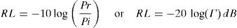 (2)
(2)
where Pi is an incident power; Pr is the reflected power and Γ is the reflection coefficient.
 (3)
(3)
The dielectric material of FR-4 Epoxy with 1.6 mm thickness is selected for this design and has a dielectric constant of 4.4(ε r ) and loss tangent equal to 0.002. Low dielectric constant is used in the prototype design because it gives better efficiency and higher bandwidth (Balanis, 2005; Ramesh, Prakash, Inder, & Apisak, 2001; Wong, 2002) and it increases the fringing field at the patch periphery and thus increases the radiated power. The small loss tangent was neglected in the simulation. Substrate thickness is another important design parameter. Thick substrate increases the fringing field at the patch periphery like low dielectric constant and thus increases the radiated power (Kraus, 1988; Raju, 2005).
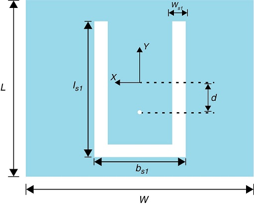
The proposed antenna is simulated using HFSS and the practical results are obtained by testing the fabricated antenna using Vector Network Analyzer (E5071C). The design of single U-slot antenna structure is presented in Fig. 1 and corresponding dimensions are length of the patch (L ) is 52 mm, width of the patch (W ) is 71 mm, length of vertical outer slot (ls 1 ) is 40 mm, length of horizontal outer U-slot (bs 1 ) is 18 mm, width of outer slot (ws 1 ) is 4 mm, and offset feed length (d ) is 9 mm.
2.1 Simulated results of single U-slot structure
Initially a single or primary U-slot is introduced on the patch as shown in Fig. 1 and the simulation results are shown in Fig. 2.
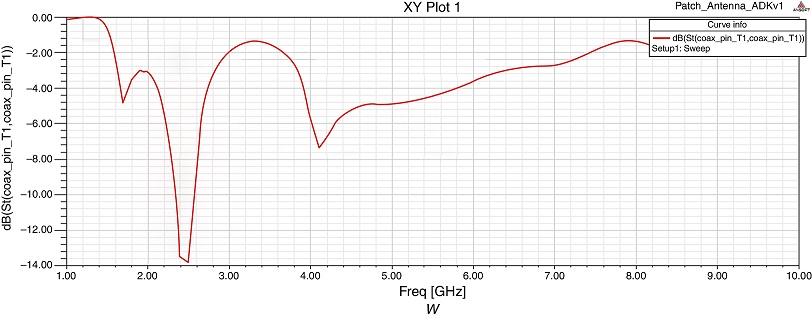
Fig. 2 shows the S11 versus frequency plot. The antenna with primary U-slot resonates at the frequency 2.5 GHz.
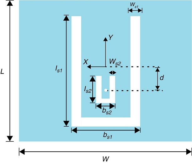
One more U-slot (secondary U-slot) is introduced inside the primary U-slot. The dimensions of the secondary U-slot are ls 2 = 13 mm, bs 2 = 4 mm, and ws 2 = 1 mm as shown in Fig. 3.
2.2 Simulated results of double U-slot structure
The patch antenna with primary U-slot resonates at single frequency. The introduction of secondary U-slot as shown in Fig. 3 provides dual band frequencies.
Fig. 4 shows the Return Loss curve of double U-slot structure. It is observed that the incorporation of secondary U-slot gives dual resonant frequencies at 1.9 GHz and 5.5 GHz.

2.3 Simulation of results by varying offset position (d)
Feed position plays a major role in the design. Probe feed is used to provide the feed to the antenna. The characteristics of antenna vary with the probe position from center of the patch toward secondary U-slot and the corresponding results are tabulated in Table 1.
Table 1 Variation of gain and frequency with feed position.
| Offset feed (d )Position (mm) | Gain (dB) | ResonantFrequencies (GHz) |
|---|---|---|
| At center (d = 0) | 5.34 | 2 |
| Moving downwards (d = 1) | 5.41 | 2, 3.1 |
| Moving downwards (d = 4) | 5.63 | 2.2, 4.8 |
| Moving downwards (d = 9) | 6.80 | 1.9, 2.1, 5.4 |
Fig. 5 shows the Return Loss curve when the feed position is at center (d = 0). It is observed that the resonant frequency is 2 GHz when feed is at the center.

The observations from the Figs. 4 and 5 and Table 1 are that the primary U-slot gives single band, secondary U-slot provides two bands and multiple bands are obtained for offset feed position (d = 9) with a gain of 6.80 dB. The gain is increasing with increase in offset feed position (d ) as shown in Table 1.
3. Triple-layer structure of the proposed antenna
The proposed design of the antenna is a combination of two U-slots and triple-layer structure as shown in Fig. 6. The height of dielectric substrate employed in this design of antenna is h = 1.6 mm for top and bottom layers. The middle layer among the three layers is taken as air and the gap between first and third layers is taken as 8.5 mm.

4. Parametric study and discussion of results
4.1 Variation of substrate material
Fig. 7 shows the S11 versus frequency plot of triple-layer structure. The effect on gain with respect to single and triple-layer is tabulated in Table 2 along with variation of substrate material.

Table 2 Comparison of gain values with substrate material and number of layers.
| Substrate material | Gain (dB)(Triple-layer) | Gain (dB)(Single layer) |
|---|---|---|
| Arlon | 7.4742 | 6.8016 |
| Dupont | 7.5634 | 5.7975 |
| FR4 | 6.5829 | 3.6454 |
| Nelco | 7.4161 | 5.6314 |
| Neltec | 7.5869 | 5.8316 |
| Taconic | 7.6323 | 6.1268 |
| Diamond pl_cvd | 7.6948 | 6.7759 |
| Polymide | 7.5561 | 6.3556 |
From Table 2 it is observed that the triple-layer structure possesses increased gain around 7.5 dB for various substrate materials like Arlon, Diamond pl_cvd and polymide, etc. Due to the non-availability and high cost of the materials, the proposed antenna is fabricated using FR4 substrate material.
4.2 Variation of gap between primary and secondary U-slots
Fig. 8 shows the Return Loss of the antenna when the gap is 5 mm and the obtained dual band frequencies are 2.2 GHz and 4.2 GHz. The effect of gain and corresponding resonant frequencies are tabulated in Table 3 with the variation of gap between primary and secondary U-slots.
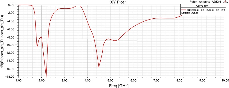
Table 3 Effect of gain and resonant frequencies with variation of gap between two U-slots.
| Gap (mm) | Gain (dB) | ResonantFrequencies (GHz) |
|---|---|---|
| 5 | 6.61 | 2.2, 4.2 |
| 4 | 6.42 | 2.1, 4.4 |
| 3 | 7.21 | 2.2, 4.5, 5.7 |
| 2 | 6.81 | 2.1, 4.8, 5.4 |
From Table 3 it is observed that when the gap is reduced from 5 mm to 1 mm successively the gain is varied around 6.6-7.5 dB and provides multiple bands at various gap dimensions.
4.3 Variation of double U-slot structure position on substrate
Varying the double U-slot structure position on substrate from center of the substrate to both upward and downward directions, and by keeping the optimum values of length, feed position, substrate material and gap between U-slots, the following results are obtained.
Fig. 9 shows the Return Loss of the antenna when the gap between patch (primary slot) and bottom edge of substrate (shifted 2 mm downwards) is 12 mm.
From Table 4 it is observed that when the gap increases the gain improved and in the same way multiple (triple and double) frequency bands are obtained.
Table 4 Effect of double U-slot structure position with respect to substrate and corresponding gain and resonant frequencies.
| Gap (mm) | Gain (dB) | ResonantFrequencies (GHz) |
|---|---|---|
| 16.00 | 7.66 | 2.2, 5.9 |
| 15.00 | 7.34 | 2.2, 4.4, 5.7 |
| 14.75 | 7.17 | 1.8, 2.2, 5.6 |
| 14.50 | 7.53 | 2.2, 4.5, 6.0 |
| 14.25 | 7.46 | 2.24, 4.5, 5.6 |
| 13.75 | 7.15 | 2.2, 4.5, 5.6 |
| 13.50 | 7.14 | 2.2, 4.8 |
| 13.00 | 6.81 | 2.2, 4.4 |
| 12.00 | 6.60 | 2.2, 4.7 |
4.4 Simulated results of variable substrate thickness
Varying the thickness of the substrate for top and bottom layers, the dual-band and sufficient impedance bandwidth characteristics are obtained. The optimum thickness of the substrate is 0.6 mm. But practically, fabrication of antenna with such less thickness is complex, so the thickness of 1.6 mm is considered. Fig. 10 and Fig. 11 show the Return Loss of antenna with thickness of 0.6 mm and 1.6 mm respectively.


From Fig. 10 the Return Loss is −17.41 dB at 1.8 GHz, −17.42 dB at 2.2 GHz and −12.1 dB at 4.8 GHz. The impedance bandwidth obtained is 800 MHz with substrate thickness of 0.6 mm. From Fig. 11 it is observed that with substrate thickness of 1.6 mm the resonant frequencies of 1.6 GHz, 1.9 GHz and 3.8 GHz are obtained.
Fig. 12 shows that the VSWR values of the proposed antenna are 1.8113 at 1.6 GHz, 1.3814 at 1.9 GHz and 1.2180 at 3.8 GHz.

From Figs. 10 and Fig. 11 it is observed that, with the variation of substrate thickness triple bands are obtained with improved bandwidth. It is difficult to provide the substrate with 0.6 mm thickness, so the design of antenna is carried out with substrate thickness of 1.6 mm. Fig. 12 shows that the VSWR is lesser than 2 at consequent resonant frequencies.
5. Fabricated structure and practical results
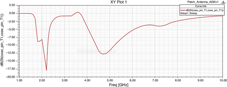
The fabricated antenna with three layers is shown in Figs. 13-15 with patch and ground planes. Fig. 16 shows the experimental setup with Vector Network Analyzer (VNA).
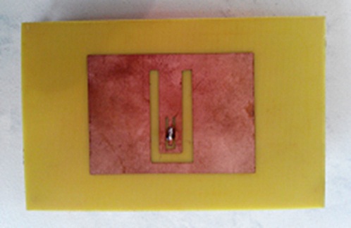
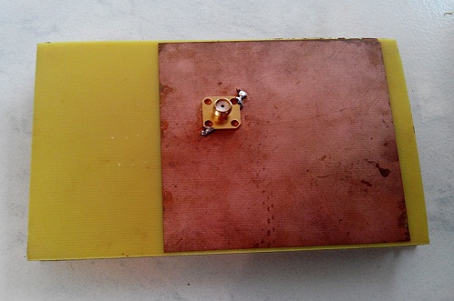
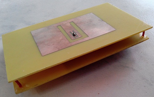

Fig. 17 shows the Return Loss curve of fabricated antenna displayed on VNA. The obtained simulated resonant frequencies are 1.6 GHz, 1.9 GHz and 3.8 GHz. The tested results of fabricated antenna with Vector Network Analyzer (VNA) are nearly same as the simulated results and they are 1.54 GHz, 1.89 GHz and 3.81 GHz. The obtained impedance bandwidth of fabricated antenna is 600 MHz from 3.6 GHz to 4.2 GHz at center frequency 3.8 GHz.
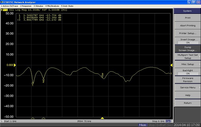
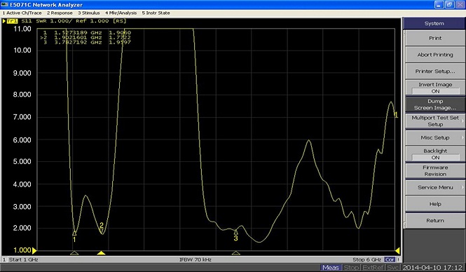
Fig. 18 shows that the VSWR values at 1.54 GHz, 1.9 GHz and 3.78 GHz are 1.906, 1.722 and 1.909 respectively.
6. Conclusions
The design of multilayer microstrip patch antenna has been proposed in this paper. The proposed triple-layer structure of the antenna can be used for multiple wireless applications. The inclusion of three layers in the antenna structure increases the bandwidth and it leads to the more coverage of frequencies. The proposed triple-layer double U-slot patch antenna is simulated in HFSS solver and fabricated using thermo-lithography process. It is observed from the extensive parametric study that the antenna possesses triple bands in most of the cases. The proposed antenna has triple bands at 1.6 GHz, 1.9 GHz and 3.8 GHz and a bandwidth of 600 MHz. The experimental results are in close agreement with the simulated results.

