


 nueva página del texto (beta)
 Inglés (pdf)
 Artículo en XML
 Referencias del artículo
 Enviar artículo por email
 Citado por SciELO
  Similares en
SciELO
Similares en
SciELO 
 Permalink
1. Introduction
CA/CA power electronic converters are highly demanded on the industry, transport and service sectors. Usually these converters have been implemented by using a two stage conversion process: a CA/CD converter followed by another CD/CA resulting in a DC bus link which needs storage energy elements such as an inductor whether the converter works as a current source converter, or a capacitor if it works as a voltage source converter.
Another way of CA/CA conversion is the Matrix Converter (MC) which is comprised by bidirectional switches (Wheeler, Clare, Empringham, Apap, & Bland, 2003). The conversion in this converter is straightforward without a DC link. Pulse width modulation (PWM) to control the switching sequence is used for the conversion process. One of the main advantages of the MC is that as it has no DC link the volume and weight of the converter are reduced due to the removal of electrolytic capacitors which contributes with 30-50% of the total volume in a conventional converter (Wheeler et al., 2003).
The use of MCs is currently limited. The main reasons are: (1) limited availability of the bidirectional power electronic devices working at high frequencies, (2) control implementation is complex, (3) the output voltage is only 86.6% of the input voltage, (4) the cost of the protection systems for the bidirectional switches is high (Podlesak et al., 2005). However with the technology progress it is expected that the MC will become a real alternative to the traditional voltage source converter (VSC). An experimental 150 kV A matrix converter has been reported in Podlesak et al. (2005). The MCs are currently used in applications such as wind power generators (Cha & Enjeti, 2003), no break energy sources (Ratanapanachote, Cha, & Enjeti, 2004), motor drives (Chekhet, Sobolev, & Shapoval, 2000) and marine propulsion drives (Dalal, Syam, & Chattopadhyay, 2006).
Simulation and experimental results of a 3 × 3 MC with input and output filters are presented and discussed in this paper. A particular four-step space vector modulation (SVM) sequence is used. Tracking (TC) and repetitive controls (RC) are used to regulate the output voltage under balanced and unbalanced load conditions.
2. 3 × 3 Matrix converter
Fig. 1 shows a 3 × 3 MC comprised by a 9 bidirectional switch array which connects the output phases a, b, or c with the input phases A, B or C. Input and output filters are illustrated as well.

Bidirectional switches are controlled under the following constraints:
As the converter is fed by a three-phase voltage source, only a bidirectional switch per output phase can be turned on to avoid a short circuit between two input phases.
As the loads are usually inductive it must be guaranteed that an output phase must be connected to an input phase at any time and abrupt changes of current must be avoided for not generating high dv /dt that may damage the switches.
Bearing in mind these two constraints an open-loop control based on SVM and a four-step switching strategy was implemented. Input and output filters were used to avoid injecting harmonic currents into the mains and harmonic voltages into the load. The SVM, four-step switching strategy, input and output filter designs are detailed next.
2.1 Space vector PWM
Space vector PWM is used in this work because it has some advantages to reduce harmonic content (THD) on the input current and output voltage (Casadei, Serra, & Tani, 1998; Casadei, Serra, Tani, & Zarri, 2009), being feasible to compensate unbalanced voltages by means of applying instantaneous voltage vectors which are calculated from the states of the switches (Casadei, Serra, Tani, & Zarri, 2002; Grzegorz, 2009; Huber & Borojevic, 1995).
2.2 Four-step current commutation
Constraints stated above must be accomplished during the commutation of one of the input phases to another input phase having the same output phase. By means of external current sensors the sense of the output-phase current of the converter is deduced, that current sense is needed to implement the commutation strategy. The commutation strategy is illustrated in Fig. 2 (Deihimi & Khoshnevis, 2009; Empringham, Wheeler, & Clare, 1998).

The procedure to disconnect input-phase A and connect input-phase B to the output-phase a accounting for the current sense illustrated in Fig. 2 (i o > 0) is as follows:
Disconnect SAa2. The load current is not interrupted.
Connect SBa1. Allowing the current to flow from input-phase B to output-phase a .
Disconnect SAa1. The switch SBa1 is closed allowing the flow of the output current.
Connect SBa2. Phase B is connected to phase a .
Delay times (t 1, t 2 and t 3) are included between step and step (see Fig. 3).
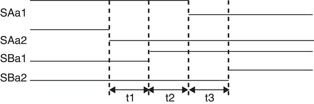
A similar analysis can be carried out for the condition i o < 0.
The switching sequence of the bidirectional switches is illustrated on the right side of Fig. 2. The state of each one of the 6 transistors is represented by "1" when the transistor is on and "0" when the transistor is off.
2.3 Input filter
In order to minimize the current harmonics injected to the mains an input filter is used (see Fig. 1). Fig. 4 illustrates the equivalent filter circuit per phase, where L and C are the inductance and capacitance of the filter, R L is the internal resistance of the inductor and R is a damping resistance (Wheeler & Grant, 1997).

The values of the components in the input filter are: L = 0.7 mH, C = 26 μF, R L = 50 mΩ, and R = 56 Ω. The transfer function (TF) of the filter is:
 (1)
(1)
Fig. 5 illustrates the Bode plot of the filter using three different damping resistances.
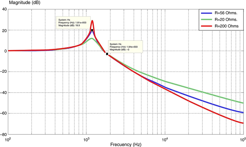
For a damping resistance of R = 56 Ω the resonance frequency is fr = 1.18 kHz and the gain is of 20 dB. Taking into account that the switching frequency of the MC is 12.8 kHz an attenuation of −40 dB is achieved. The value of R chosen results in a good balance between the amplification at frequencies close to the resonance frequency and attenuation at high frequencies.
2.4 Output filter
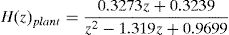
The output filter is used to reduce the voltage harmonics in the load due to the commutation of the bidirectional switches. Fig. 6 illustrates the equivalent circuit per phase for the output filter (Dewan & Ziogas, 1979; Kim, Choi, & Hong, 2000).

The values of the components in the output filter are: L = 0.128 mH, C = 68 μF and R L = 50 mΩ. The TF of the filter is:
 (2)
(2)
Fig. 7 illustrates the Bode plot of the TF, it can be seen that the cutoff frequency is 2.65 kHz for the capacitor value proposed and the resonant frequency is 1.71 kHz with a gain of 28.5 dB.

If the capacitor value is increased as shown in Fig. 7, the width band is reduced being that the reason to choose a capacitor of 68 μF.
3. Control of the matrix converter
In order to control the output voltage of the MC and to compensate the unbalanced output voltages for unbalanced loads, two different types of controllers: tracking and repetitive controllers are implemented.
3.1 Tracking control
The output voltage is the variable to be controlled with the tracking control (TC) its value is measured at the terminals of the output-filter capacitor and it is the feedback signal. The TF of the output filter (Eq. (2)) is considered as the plant for the TC. Applying z -transform to Eq. (2) results as follows:
 (3)
(3)
From Eq. (3) the characteristic equation can be obtained being theirs poles p 1,2 = 0.4949 ± 1.0237j which are located out of the unit circle. In order to improve the control system stability these poles have to be canceled with the zeros of the controller resulting in a TF for the controller with new stable poles as follows:
 (4)
(4)
Sisotools of Matlab v7.6 was used for the TC design. Fig. 8 illustrates the block diagram of the TC.

Fig. 9 shows the Bode plot of the controller. It can be seen that the controller attenuates the peak value of the gain (see Fig. 7) at the resonance frequency of 1.71 kHz of the output filter (plant).

From Eq. (4) and the block diagram of Fig. 8 a recursive equation (Eq. (5)) can be deduced. The MC control is based on Eq. (5) which is programmed in a DSP.
 (5)
(5)
where
 (6)
(6)
k - is an integer value (number of sample), V (k ) ref , V (k ) fb - are the reference and output values respectively for a k sample, U (k ) - is the subtraction of V (k ) ref , from V (k ) fb , Y (k ) - is the output variable of the controller.
3.2 Repetitive control
Repetitive control (RC) is used to change the reference value applied to the TC to reduce the noise at the output and diminish the periodical errors that can appear in the control loop (Inoue, 1990; Yeh & Tzou, 1995). Fig. 10 shows a block diagram of the RC where: r (z ) is the reference signal, e (z ) is the error signal, Z − N is the delay in the feedback loop, N is the number of samples in a period of the fundamental frequency, Q (z ) is a constant, S (z ) is a low-pass filter that works as compensator providing robustness to the control system and improving the stability margin, Z − k is a delay to make the output signal of the block C (z ) to be in-phase with the input signal r (z ), K r is the gain of the RC, r c (z ) is the modified reference, P (z ) is the TF of the TC and it is considered as the plant (output filter) of the control, C (z ) is the polynomial transfer function for the RC and Y (z ) is the output.

The polynomial C (z ) is as follows:
 (7)
(7)
The value of Q (z ) in Fig. 10 is a constant equal to 0.95 (Zhang, Kang, Xiong, & Chen, 2003). The compensator S (z ) is a second order IIR filter (García-Cerrada, Pinzón-Ardila, Feliu-Batlle, Roncero-Sánchez, & García-González, 2007) with a cutoff frequency of 400 Hz (fundamental frequency of the MC output) and a sampling frequency of 12.8 kHz which is equal to the switching frequency of the MC. The Matlab toolbox "fdatool" is used for the design of the filter. The TF of the filter is:
 (8)
(8)
Fig. 11 shows its Bode plot. The value of N is the ratio between the switching and fundamental frequencies. N = 12,800/400 = 32. The value of K r is 0.6 (García-Cerrada et al., 2007; Zhang et al., 2003). The procedure for computing the value of k is based on a simulation where the output of C (z ) and the reference signal r (z ) are compared (Fig. 10), k is adjusted until the mismatch between C (z ) and r (z ) is compensated. The value of k found is equal to 23 therefore Z − k = Z −23.

The final diagram of the RC is shown in Fig. 12. A delay Z −1 is added to the reference signal to guarantee that this signal is in-phase with the feedback signal.
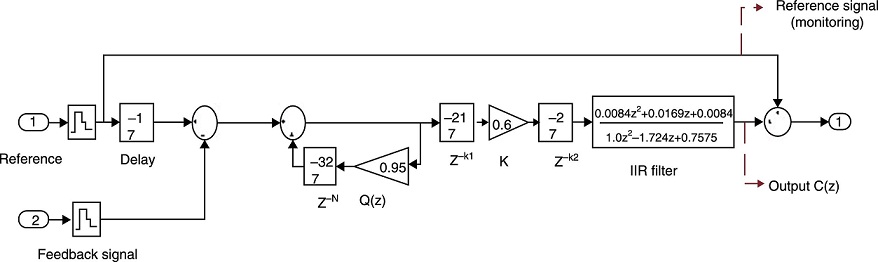
By splitting Fig. 12 in three sections the recursive equations are deduced as follows:

 (9)
(9)

 (10)
(10)

 (11)
(11)
4. Simulation results
The 3 × 3 MC was simulated in Matlab/Simulink v.7.6. Fig. 13 illustrates the a-phase current and the switch states for a 4-step commutation (see Fig. 1). Fig. 14 shows the MC output voltages per phase, a three-phase unbalanced star connected resistive load of 4 Ω, 8 Ω and 10 Ω was used.


Fig. 14 Open loop output voltages with unbalanced load and filters (a), adding TC (b), adding TC+RC (c); output currents with TC+RC (d).
Fig. 14a shows the output voltages per phase of the MC in open loop, the output and input filters are connected. This figure shows the unbalanced shape of the voltages due to the unbalanced load.
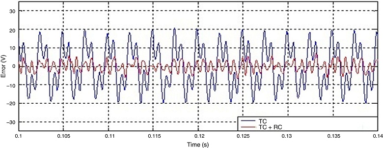
Fig. 14b shows the results after adding a TC to control the output voltage. The stability was improved as it was pointed out above however the waveforms are still unbalanced. Finally Fig. 14c illustrates the results of adding an RC to control the output voltage. A balanced output voltage is achieved despite the unbalanced load used. The output currents with TC + RC are shown in Fig. 14d. In addition to get balanced output-voltages when RC is added to the control system a reduction on the error of the output voltage of the MC is achieved. Fig. 15 illustrates the output voltage error under TC and TC + RC. The error is calculated as the subtraction of the output voltage measured at the output capacitor from the reference voltage.
5. Hardware implementation
With the aims of validating the control of the MC a laboratory prototype was built. Fig. 16 shows the laboratory setup. It can be seen the input and output filters, the MC and the control boards which are comprised by a development kit DSP TMS320C6713, communication board HPI (Host Port Interface) and an FPGA board. The printed circuit board of the MC and FPGA were designed by The Nottingham University in the UK (Buso & Mattave, 2006) and these were acquired for this project. The communication board HPI allows the data transmission between PC and DSP using an USB port being possible the monitoring of different variables in de DSP by using an interface developed in Matlab. The rated output power of the MC is of 7.5 kW. It is comprised by 12 bidirectional switches in a matrix array of three rows by four columns (only three columns were used in this work). Each bidirectional switch is comprised by two IGBT transistors and isolated gate drivers. Each output phase has attached a current sensor used to implement the 4-step commutation.

6. Experimental results
Fig. 17 shows the experimental results for the MC without input and output filters. It can be seen a high frequency harmonic content due to the switching devices. Fig. 18a shows the phase voltage and output line-currents with a Y-connected resistive load. Fig. 18b illustrates a phase of the input current. Input and output filters are connected to the MC for results of Fig. 18 and Fig.19 show output voltages and currents per-phase for an unbalanced 3-phase Y-connected resistive load of 4 Ω, 8 Ω and 10 Ω. By analyzing this figure it can be seen that the voltage peak values are of 80 V being of the same value as the reference value validating the simulating results shown in Fig. 14c.

Fig. 17 Output signals without filters: phase voltage (a), currents (b), line voltage (c), input current (d).


The output currents have different maximum values: 13.9 A, 10.6 A and 9.3 A due to an unbalanced load and their values correlate well with those shown in Fig. 14d.
7. Conclusions
The AC/AC power conversion in a MC is straightforward without needing to carry out a two-stage conversion process resulting in a converter without a DC bus link and in consequence a storage energy element is needless. MC is comprised by a bidirectional switch-array; the number of switches relies on the type of matrix. The bidirectional switches need a high performance switching control to avoid operational fails. In this work the simulation and experimental validation of a 3 × 3 MC were carried out assessing the output voltage regulation for balanced and unbalanced loads. A 4-step commutation was assessed resulting in a safe operation in the MC. Input and output filters were used to avoid injecting harmonic currents into the mains and harmonic voltages into the load. The compensation of the voltage control loop was carried out by a TC where the poles of the TF of the output filter were canceled with the zeros of the controller increasing the system stability. By means of the RC the reference signal applied to the TC can be varied to reduce the noise at the output and diminish the periodical errors that can appear in the control loop. The experimental results illustrate that the output voltage amplitudes correlate well with the reference signal when TC + RC are used even though unbalanced loads are connected.

