


 nueva página del texto (beta)
 Inglés (pdf)
 Artículo en XML
 Referencias del artículo
 Enviar artículo por email
 Citado por SciELO
  Similares en
SciELO
Similares en
SciELO 
 Permalink
1. Introduction
Nowadays, most successful implementations obtained in asynchronous microprocessors have been developed at the ASIC level. Asynchronous design has been used from the beginning of the computer age, even before the VLSI technology was possible. Due to the introduction and advances of integrated circuits, the paradigm of synchronous design became popular and came to be the dominant design style (Chu & Lo, 2013). However, in recent years, asynchronous design has had a comeback in ASIC implementations (Beerel, 2002; Lavagno & Singh, 2011; Smith, Al-Assadi, & Di, 2010).
Programmable devices are an excellent option for developing cheaper and faster digital circuit prototypes, due to their great integration capability and flexibility. In that context, asynchronous design can be performed using FPGAs devices. To make this platform practical and useful to the asynchronous design, some Self-Timed (ST) control block techniques and steady/latch delays are required. This allows us to build the ST synchronization circuits. Most of the microprocessors are made with a global clock synchronization system, in which the whole or part of the circuit is subject to a unique pulse line, which distributes and synchronizes data transfer. In addition, synchronous microprocessors that use a single clock can bring about various problems due to the high demand of processing. To overcome this problem, asynchronous systems are proposed, since in an ST synchronization system, the control of data transfer between blocks is regulated through local signing lines that indicate the request and data transfer between contiguous blocks. Since these types of systems do not depend on a global clock, they take full advantage of the speed and energy consumption when implemented in programmable devices. Asynchronous systems are relatively new, but they present better performance than their homologous synchronous systems. Moreover, microprocessors with asynchronous systems can be easily implemented in FPGAs (Ortega-Cisneros, Raygoza-Panduro, & de la Mora-Gálvez, 2007; Tranchero & Reyneri, 2008).
This paper presents the design, implementation, and experimental results of an asynchronous 32-bit microprocessor implemented in a Xilinx FPGA Virtex 5 that are developed in a platform designed exclusively for synchronous circuits (Xilinx Inc., 2015). The FPGAs uses synchronous components, such as DCM (digital clock manager) and DLL (delay-locked loop) utilized by the software tools in order to synthesize a design. This implementation can be performed by means of a ST pipeline as an activation signal generator block, as well as the hard macro needed to generate the delay time for the ST asynchronous protocol.
2. Background of Self-Timed circuits
The potential benefits of asynchronous logic have caused a resurgence of interest in the design methodology of these systems, which have received an important boost in recent years (Edwars & Toms, 2003; Geer, 2005). Recent initiatives in the industrial field include smart cards from Philips (Yoshida, 2003), Sun (Johnson, 2001), and Sharp (Terada, Miyata, & Iwata, 1999). There are many important research groups specializing in asynchronous microprocessors (Werner & Akella, 1997). This section describes the architecture and design style of some of these. Table 1 summarizes the main features.
Table 1 Asynchronous microprocessors.
| Microprocessor | Architecture | Technology | Performance |
|---|---|---|---|
| Caltech (Martin, Burns, Lee, Borkovic, & Hazewindus, 1989) | 4-phase, dual rail, 5-stage pipeline, 16-bit RISC. | 20,000 1.6 μm transistors | 18 MIPS |
| NRS (Brunvand, 1993) | 2-phase, single rail, 5-stage pipeline, 16-bit RISC. | FPGA Actel | 1.3 MIPS |
| AMULET1 (Furber, Day, Garside, Paver, & Woods, 1994) | 2-phase, single rail, 5-stage pipeline, based on a 32-bit ARM. | 60,000 1.0 μm transistors | 9k Dhrystones |
| TICTAC 1 (Murata, 1989) | 2-phase, dual rail, 2-step non-pipeline, 32-bit RISC. | 22,000 1.0 μm transistors | 11.2 MIPS |
| FRED (Richardson & Brunvand, 1996) | 2-phase, single rail, multifunctional pipeline, based on a 16-bit 88100. | Defined in VHDL | 120 MIPS |
| 80C51 (van Gageldonk et al., 1998) | 4-phase, single rail, CPU and peripherals, 8-bit CISC. | 27,4820 1.6 μm transistors | 2.10 MIPS |
| AMULET2 (Furber et al., 1999) | 4-phase, single rail, forwarding pipeline, based on a 32-bit ARM. | 450,000 0.5 μm transistors | 42 MIPS |
| TICTAC 2 (Takamura et al., 1998) | 2-phase, dual rail, 5-stage pipeline, based on a 32-bit MIPS R 3000. | 496,000 0.5 μm transistors | 52.3 VAX MIPS |
| AMULET3 (Furber, Edwards, & Garside, 2000) | 4-phase, single rail, forwarding pipeline, based on a 32-bit ARM. | 113,000 0.35 μm transistors | 120 MIPS |
| BitSNAP (Ekanayake, Nelly, & Manohar, 2005) | 4-phase, dual rail, based on 16, 32, and 64-bit SNAP ISAs | 0.18 μm CMOS | 6-54 MIPS |
| NCTUAC18S (Hung-Yue, Wei-Min, Yuan-Teng, Chang-Jiu, & Fu-Chiung, 2011) | 4-phase, dual rail, 5-stage pipeline, based on and 8-bit PIC18 ISA. | 0.13 μm TSMC | n/a |
The microprocessors described in Table 1 can be broadly divided into two categories:
Those constructed using a conservative time model, suitable for formal synthesis or verification, but with a simple architecture: TITAC.
Those constructed using less care in the time models, with an informal design approach, but with a more ambitious architecture: AMULET, NSR, FRED.
Another consideration that may be taken to evaluate the implementation of asynchronous circuits in the area of microprocessors, is the type of application and implementation:
Microprocessors used in commercial applications: AMULET, Philips 80C51.
Those implemented in full-custom: Caltech, TICTAC.
Those that have only been proposed: FRED.
Fig. 1 shows a power consumption graph, where the power range is between 9 mW and 2 W.

3. Self-Timed microprocessor architecture
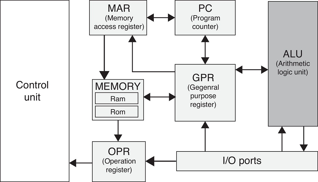
Characteristics and components of the ST microprocessor are defined in this section. The fundamental parts are the delay block and the control unit, which activates all the microprocessor blocks and gives a sequence of how to execute each instruction. Fig. 2 shows the ST microprocessor diagram.
3.1 Asynchronous microprocessor structure
The ST control unit is based on FIFOs that contain micropipelines of asynchronous control blocks (ACB) using the 4-phase single rail protocol (Jung-Lin, Hsu-Ching, Chia-Ming, & Sung-Min, 2006; Ortega, Gurrola, Raygoza, Pedroza, & Terrazas, 2009). This protocol is used because communication is more effective than 2-phase single rail protocol on FPGAs, as it fulfills the necessary characteristics for substituting synchronous FIFOs. The 2-phase protocol uses fewer transactions and requires less energy consumption than the 4-phase. However, the latter ensures a stable asynchronous communication and is better adapted to the requirements of circuits that use latches. The 4-phase protocol occupancy is smaller than 2-phase, because an ACB implementation for the first requires fewer components than the second. Also, single rail requires less hardware than dual rail protocols.
The ST microprocessor developed in this work is a general purpose design. It is controlled with an asynchronous block that orders the data flow through all the logic components. The ST microprocessor is based on micropipeline structures that generate activation pulses toward different modules, using the 4-phase protocol. The first element described is the control unit, shown in Fig. 3. It uses asynchronous control blocks along with delays to adjust the time required for the request signal between each ACB. Compared with synchronous controllers, which depend on the slower process in order to optimize the clock speed, asynchronous versions improve the delay from each individual process to the minimum possible and reduce the program time execution.
3.2 Asynchronous control unit
An explanation of changing synchronous FIFOs for asynchronous is given here. Flip Flops (FF) are replaced by ACBs. Thus, instead of having a clock signal that activates each FF, a request signal is send sequentially to all ACBs.
Fig. 4 shows the asynchronous FIFO that corresponds to the fetch cycle. The time for the request to go through all X signals is determined by a hard macro delay block implemented with the Xilinx FPGA Editor tool. The delay consists of a single LookUp-Table (LUT) assigned as a buffer (Ortega, Raygoza, & Boemo, 2005). With this macro, it is possible to implement Self-Timed designs on synchronous FPGAs. The FIFO uses 4 ACBs in a micropipeline to generate the signals that activate the fetch cycle.

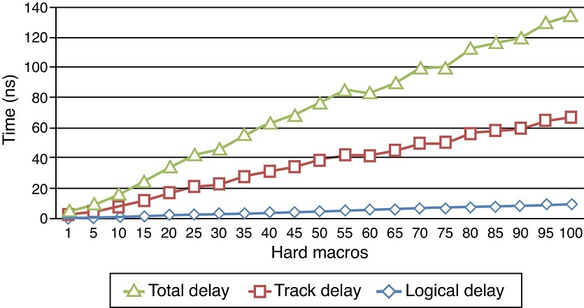
One important problem emerges when the designer uses exactly the same number of delay macros needed to achieve a specific time accorded to a specific delay graph. When trying to implement the design into the FPGA, the time generated from the automatic routing of the software may be different every time. As a consequence, the design will not work properly, since the delay macro time could be lower than the expected value. In order to avoid this problem, a place and route restriction is recommended in order to ensure the same delay time in each design synthesis. In addition, the sum of the logic delay and track delay must be greater than the delay of the processing logic function implemented in order to ensure stability of the output of the synchronizing circuit before a new entry is applied. Fig. 5 exhibits linear logic and non-linear track delays generated by the macros.
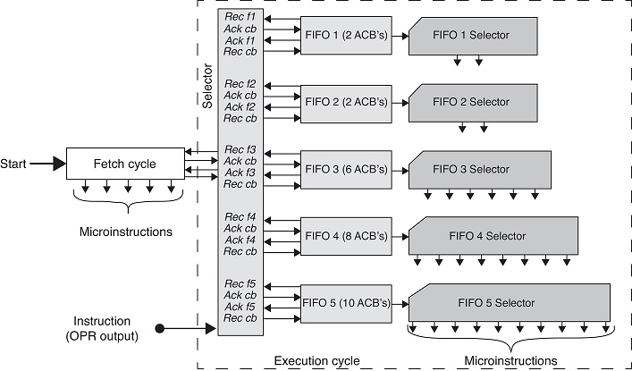
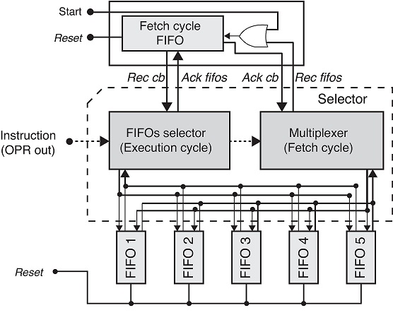
The selector shown in Fig. 6 is a decoder that indicates which of the 5 FIFOs blocks of the executing cycle is going to perform the instruction. This decoder sends a request to the chosen FIFO and awaits the acknowledgment signal; it also transmits the request to the fetch cycle when the execution cycle ends. In the asynchronous controller, this selector also performs the same process as the synchronous controller, i.e., loading a data and an instruction from port Sum (LPS). After the instruction LPS has been performed, the selector returns a request to the execution cycle in order to be able to execute another instruction. FIFOs execution cycle instruction selectors are the same as in the synchronous controller.
3.3 Signals that activate the FIFOs of the asynchronous controller
Since asynchronous FIFOs can wait the necessary time to deliver the next request, they may be optimized. In the synchronous version, some instructions require skipping one clock pulse, because of the waiting time, as the extra period required for complex operations in order to finish their processes. All execution FIFOs have a different quantity of ACBs (or FF for synchronous FIFOs), which depend on the complexity of the instructions and the number of activation signals. Each FIFO is used to execute different instructions in order to save FPGA area or hardware. Fig. 3 shows a microinstruction selector for each FIFO block.
Table 2 shows three examples of instructions with their corresponding FIFOs. From left to right: the mnemonic of the instruction (MNE), the FIFO that can execute the instruction, the number of the ACB that activates each signal, and the activated signals (microinstructions). The instructions presented are: accumulator complement (NAC), load direct memory to accumulator (LDA), and subroutine call (CSR). In order to know the time each fetch or execution cycle takes, it is necessary either to implement the design on the FPGA and get a timing analysis or simulate a program in the microprocessor. This is noteworthy, since in the synchronous design only the clock frequency must be known.
Table 2 Signals that activate asynchronous instructions.
| MNE | FIFO | N° ABC | Signals |
|---|---|---|---|
| NAC | 1 | 1 | Compl_acc |
| 2 | Acc_clk | ||
| LDA | 4 | 1 | Gpr_mar |
| 2 | Mar_clk | ||
| 3 | Ram_clk | ||
| 4 | M_gpr | ||
| 5 | Gpr_clk | ||
| 6 | Time to process | ||
| 7 | Load_gpr | ||
| 8 | Acc_clk | ||
| CSR | 5 | 1 | Gpr_mar |
| 2 | Mar_clk | ||
| 3 | Pc_gpr | ||
| 4 | Gpr_clk | ||
| 5 | Mar_pc | ||
| 6 | Pc_clk | ||
| 7 | W_ram | ||
| 8 | Ram_clk | ||
| 9 | Inc_pc | ||
| 10 | Pc_clk |
4. Microprocessor instructions
4.1 Arithmetic Logic Unit
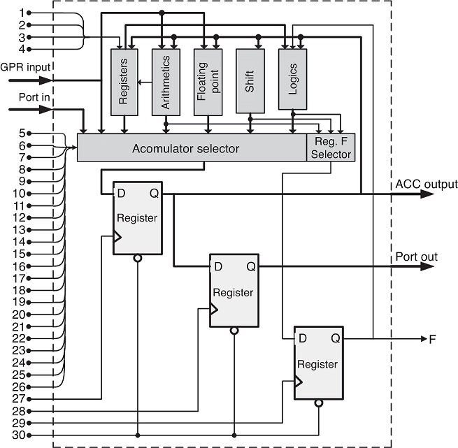
The Arithmetic Logic Unit (ALU) is an important part of the microprocessor, as it develops all the operations between data. These operations are logical, arithmetic, ports and registers access, floating point arithmetic, and bit shifting. These operations are performed in parallel and a selector is used. The result of the desired operation is chosen and the output of this selector is stored in a register called the accumulator (Acc). The ALU uses 32-bit data to perform the operations. Data may be received from the General Purpose Register (GPR), the input port (Port in), and the internal registers. The latter are used to store the information to be processed immediately. Also, the ALU contains a one-bit flag (register F), which stores the carry generated by arithmetic and shift operations. The block diagram of the ALU is shown in Fig. 7.
The ALU was designed to perform 29 operations and the general reset. The operations are shown in Table 3. A brief explanation of the floating point operations that the ALU performs are presented later.
Table 3 Arithmetic Logic Unit operations.
| N° | Signal | Process |
|---|---|---|
| 1 | Regx_clk | RegX = 0, Register X clock |
| 2 | Regy_clk | RegY = 0, Register Y clock |
| 3 | RegHi_clk | RegHi = 0, Register High clock |
| 4 | RegLo_clk | RegLo = 0, Register Low clock |
| 5 | Dec_acc | Acc = Acc − 1 |
| 6 | Add_gpr | Acc = Acc + GPR, F = Carry |
| 7 | Load_gpr | Acc = GPR |
| 8 | Rotate_Right | Acc = {Acc[n-1:0], Acc[n]} |
| 9 | Rotate_Left | Acc = {Acc[0], Acc[n:1]} |
| 10 | Compl_acc | Acc = ∼Acc |
| 11 | Shift_Right | Acc = {Acc[n-1:0], 1′b0}, F = Acc[n] |
| 12 | Comp_regx | Acc = Acc = |
| 13 | Inc_acc | Acc = Acc + 1, F = Carry |
| 14 | Load_regx | Acc = RegX |
| 15 | Load_regy | Acc = RegY |
| 16 | And_xy | Acc = RegX And RegY |
| 17 | Or_xy | Acc = RegX Or RegY |
| 18 | Load_Pin | Acc = Port_in |
| 19 | Subt_gpr | Acc = Acc - GPR |
| 20 | Multp_gpr | {RegHi, RegLo} = Acc * GPR |
| 21 | Shift_Left | Acc = {1′b0, Acc[n:1]}, F = Acc[0] |
| 22 | MultpHi_gpr | Acc = RegHi |
| 23 | MultpLo_gpr | Acc = RegLo |
| 24 | Addpf_gpr | Acc = Acc + GPR, floating point |
| 25 | Subtpf_gpr | Acc = Acc − GPR, floating point |
| 26 | Multppf_gpr | Acc = Acc * GPR, floating point |
| 27 | Acc_clk | Acc = 0, Accumulator clock |
| 28 | Pout_clk | Port_out = Acc |
| 29 | F_clk | RegF = 0, Register F clock |
| 30 | Reset | General Reset |
4.2 Floating point arithmetic operations
The floating point operations that the ALU performs are: addition, subtraction, and multiplication. These operations are based on Floating-Point Arithmetic IEEE 754-2008 (IEEE, 2008) with 32-bit simple precision.
The adder-subtractor design can be seen in Fig. 8 (Raygoza, Ortega, Carrazco, & Pedroza, 2009). The first step is to identify the type of data that are present in the input, as proposed in Table 4. The second step is to send the data to one of the 4 blocks that perform the addition, depending on the type of data. Then, the exponents are aligned with the same value. After that, depending on the sign of the data, addition or subtraction of mantissas is executed. In the special case in which data do not represent any particular number, such as infinite ones, zero and NaN, the recommendation is to employ the symbolic operation block. The final step is to choose the correct output with the multiplexer.
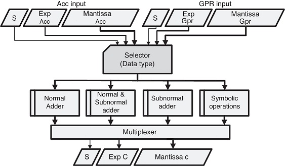
Table 4 Identification of data type in floating point.
| Data type | Identification |
|---|---|
| Zero | 3′b000 |
| Subnormal | 3′b001 |
| Normal | 3′b10X |
| Infinite | 3′b110 |
| NaN | 3′b111 |
The design and steps of the floating point multiplier are shown in Fig. 9 (Ortega, Raygoza, Pedroza, Carrazco, & Loo-Yau, 2010). The first step is to identify the data type. In the second step, the mantissas multiplication and exponent addition are performed. In the case that both inputs are infinite, zeros or NaNs, the multiplication operation is performed through the symbolic operation. In the last step, the data output could be normalized. This adjustment is done with the idea of obtaining a normal number as a result.

Compared to the arithmetic multiplier, the floating point multiplier delivers a 32-bit result. The results of the adder-subtractor and the multiplier go directly to the selector. From there, the accumulator can choose them.
5. Implementation results
This section compares the occupations, power consumption, and components between asynchronous and synchronous microprocessors on a Virtex 5 FPGA (ML501). Simulations are performed and tested in real time. The times the fetch and execution cycles take for each microprocessor are obtained. Performance results of both microprocessors are presented with a test program.
5.1 Occupation
Table 5 reports the occupation only for the control units of the asynchronous and synchronous systems. The common occupations of the other microprocessor components are shown in Table 6. The DSPs blocks are used to accelerate the processes, for example, floating point arithmetic operations in the ALU. The embedded RAM memories from Virtex 5 are used to implement the main memory of both microprocessors. If the main memory is designed using LUTs (distributed RAM), FPGA resources increase considerably. As mentioned above, the PC, GPR, OPR, ALU blocks, and the memory are shared in both processors; consequently the resulted occupations are mentioned only once.
Table 5 FPGA occupation for asynchronous and synchronous control units.
| Component | LUT | Slices | Regs. | Macros |
|---|---|---|---|---|
| Available | 28,800 | 7200 | 28,800 | 28,800 |
| Synchronous | 117 | 30 | 46 | 0 |
| Asynchronous | 197 | 50 | 11 | 163 |
Table 6 Occupation of common components on Virtex 5 FPGA.
| Cmp. | LUTs | Slices | Regs. | DSP | RAM |
|---|---|---|---|---|---|
| Free | 28,800 | 7200 | 28,800 | 48 | 48 |
| PC | 34 | 9 | 32 | 0 | 0 |
| GPR | 40 | 10 | 33 | 0 | 0 |
| MAR | 34 | 9 | 32 | 0 | 0 |
| OPR | 6 | 2 | 6 | 0 | 0 |
| Memory | 0 | 0 | 0 | 0 | 2 |
| ALU | 3410 | 853 | 169 | 6 | 0 |
Table 7 shows the occupation of all elements of the asynchronous and synchronous microprocessors. Note that the differences of the final occupations are considerably lower.
5.2 Simulation
This subsection shows some simulations of both microprocessors on Virtex 5 FPGA. In order to measure the timing of each execution FIFO and the fetch FIFO, signals c_fetch and c_execution were implemented to show the start point of each stage. In these simulations, the OPR, PC, Acc, input and output port were monitored, along with the fetch and execution start signals.
Fig. 10 shows a simulation that includes the measured fetch cycle for the synchronous microprocessor working at 50 MHz. The fetch cycle was 38.988 ns. The process performed in this simulation is as follows: First, from the output port, a data was loaded into the accumulator (instruction 0E); then, the accumulator was complemented (instruction 01); and finally, the result was placed in the output port (instruction 0F).

Fig. 11 shows a simulation that includes the fetch cycle measure for the asynchronous microprocessor. The fetch cycle was 25.648 ns. This time was 13.34 ns less than the synchronous version. The developed process is similar to that in Fig. 10.

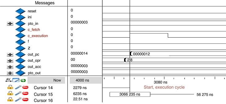
Fig. 12 presents a synchronous microprocessor simulation, in which an instruction carried out by FIFO 5 was used, and the time that it takes to perform the corresponding execution cycle was 100.671 ns. The process this simulation performs is described below. The data were loaded from the output port into the accumulator (instruction 0E); afterwards, using the memory content (zero), an indirectly floating point addition was performed (instruction 28); finally, the result was moved to the output port (instruction 0F).

Fig. 13 shows an asynchronous microprocessor simulation. The time that FIFO 5 takes to realize the corresponding execution is 56.275 ns. The developed process is similar to that in Fig. 12. A complete graph with all FIFOs is shown later.
5.3 Real time implementation
This subsection analyzes fetch and execution cycles of both microprocessors when implemented in real time on Virtex 5. The processes and the instructions that were tested are the same as those used in the simulation of Figs. 10 and 11. In real time, only the last 8 bits are shown (in hexadecimal) for each of the monitored signals, since the card ML501 has only 32 user pins, and the rest are used to connect several peripherals to the FPGA.
Fig. 14 and Fig. 15 present the processes in real time for each microprocessor. They report the timing of the fetch cycles. The time was 40 ns and 16 ns for the synchronous and asynchronous, respectively.
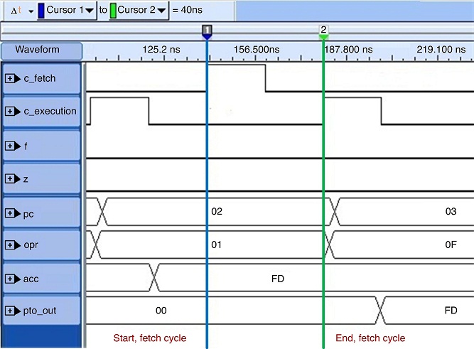
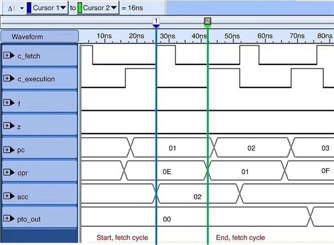
Fig. 16 presents a graph with simulation times for each cycle of both microprocessors as well as in real time. It is worth noting that for the asynchronous microprocessor there is a wider difference between the simulation and the real time, while for the synchronous microprocessor there are not considerable differences, since simulations and real time implementation work at the same clock speed (50 MHz).

The measurements obtained in real time are the most precise, since they were obtained directly from the FPGA. The next performance measures are based on resulted timing from the implementation in real time.
5.4 Power consumption
Table 8 reports the microprocessors power consumption in the FPGA (Hasan & Zafar, 2012). The measurements were performed with the Xpower Analyzer of Xilinx, which delivers measurements of the FPGA in stable state. Table 8 reports a lower consumption in the asynchronous microprocessor. However, this difference is not significant, as both microprocessor occupations in the FPGA are similar. The Xpower Analizer tool present the maximum power consumption.
Table 8 Microprocessors power consumption (mW).
| Measure | Synchronous | Asynchronous |
|---|---|---|
| Clocks | 11.43 | 7.15 |
| Logic | 0.07 | 0 |
| Signals | 1.27 | 1.26 |
| IOs | 2.71 | 0.63 |
| Total idle | 422.53 | 422.44 |
| Total dynamic | 15.47 | 9.04 |
| Total power | 438.01 | 431.48 |
In order to evaluate the power consumption in real time, an instrumentation and measurement workstation is set to obtain a better comparison between both microprocessors. The evaluation includes the ML501 board, and not only the FPGA, as in the Xpower Analyzer case, so the values obtained will be of different ranges. However, the difference in consumption between the two microprocessor versions can be seen in real time.
The power behavior of the circuits implemented in the FPGA is monitored with the current probe and a data graphic is stored. Circuit measurements are performed with the following criteria:
Circuit activity is observed through the current behavior in the main power line of the evaluation card with a current probe and an ammeter.
The capture of instantaneous measurements of current is synchronized with a digital oscilloscope, taking into account the initial trigger generated each time a program is executed.
A connection diagram with the current probe and the evaluation board is shown in Fig. 17. The probes are electrically circuit isolated, i.e., this instrument indirectly detects the current variations through magnetic field changes in the power line.

The current behavior in the evaluation board with the FPGA presents three distinctive levels:
The level without programming the FPGA.
The average level of power consumption when the device is configured.
The level when the microprocessors are working.
Fig. 18 shows a measurement graph, which indicates the three operating levels with the numbers 1, 2, and 3.

Fig. 19 shows the behavior of the asynchronous and synchronous microprocessor currents. In the latter, the activity has a global clock dependence and is more uniform throughout the circuit. In addition, it does not present changes as large as its counterpart asynchronous, i.e., once the synchronous microprocessor executes the program, the trigger levels reach their peak and then the current level falls slightly and continues permanently at a high level. If the two regions under both microprocessors lines are compared, it is seen that the area under the asynchronous microprocessor line is lower than the synchronous.

In the case of the ST microprocessor, activation levels are not dependent on a global line and tend to be more localized and appear only when a program is executed. This quality allows more controlled and optimized levels of activity, thereby enabling the reduction of power consumption.
The average current level when the FPGA is not programming was 600 mA, and 680 mA when the device is configured and inactive. The level when a program is executed in both microprocessor was 890 mA. When the asynchronous microprocessor finished the task, the current consumption was lowered to 680 mA, and in the synchronous version, to 850 mA.
From the current behavior of both circuits, and by the consideration that each microprocessor has a representative current consumption area, as shown in Fig. 20, it can be assumed that the area A st belongs to the asynchronous version and B s represents the synchronous area, therefore, Eq. (1) is the consumption difference.
 (1)
(1)

This represents the power saved by the asynchronous microprocessor.
5.5 Test programs for the synchronous microprocessor
A method to calculate the microprocessor performance is to measure the time that a program takes to be executed on it. For the evaluation, some performance test programs or benchmarks are used. Then, the evaluation continues with a program that consists of several FIFO 1 operations. Table 9 shows the test program instructions, which performs the following steps: first it clears the accumulator, then, it loads a data from the input port and finally, it shifts the accumulator seven times and sends the results to the output port.
Table 9 Test program for the microprocessor.
| N° | Address | Instruction | FIFO |
|---|---|---|---|
| 1 | 000 | 0 → acc | 1 |
| 2 | 001 | pto_in → acc | 1 |
| 3 | 002 | acc → pto_out | 1 |
| 4 | 003 | acc shift left | 1 |
| 5 | 004 | acc → pto_out | 1 |
| 6 | 005 | acc shift left | 1 |
| 7 | 006 | acc → pto_out | 1 |
| 8 | 007 | acc shift left | 1 |
| 9 | 008 | acc → pto_out | 1 |
| 10 | 009 | acc shift left | 1 |
| 11 | 00A | acc → pto_out | 1 |
| 12 | 00B | acc shift left | 1 |
| 13 | 00C | acc → pto_out | 1 |
| 14 | 00D | acc shift left | 1 |
| 15 | 00E | acc → pto_out | 1 |
| 16 | 00F | acc shift left | 1 |
| 17 | 010 | acc → pto_out | 1 |
The following equations were used to evaluate the performance of both microprocessors (Hennessy & Patterson, 2011, Ch. 1).
 (2)
(2)
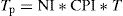
Considering the synchronous test program in Eq. (2), the cycles per instruction (CPI) of each instruction (I) indicates the cycles that FIFO 1 takes to execute the instruction (one cycle) plus the fetch cycle (two cycles). Applying Eq. (2), the CPI was 3.
 (3)
(3)
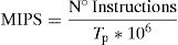
Eq. (3) was used to find the program time (T p ) for the synchronous program test. T is the clock period (20 ns for 50 MHz clock) and NI the number of instructions. The T p obtained was 1.020 μs.
 (4)
(4)
Eq. (4) calculates the MIPS (Millions of Instructions Per Second) applied in order to compare the performance between both microprocessors running the same test program. The MIPS for the asynchronous and synchronous microprocessors were 4.009 and 1.666, respectively.
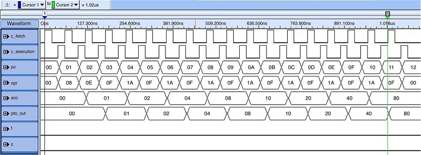
The program in Table 9 was performed in real time, shown in Fig. 21, for the synchronous microprocessor implemented on Virtex 5. Note that the time program (T p ) was 1020 ns, the same obtained by Eq. (3). Fig. 22 shows the same program of Table 9, but now with the asynchronous microprocessor prototyped on Virtex 5. In this case, the T p was 424 ns.

6. Conclusions
This work presents a Self-Timed microprocessor design compared with a synchronous version. Experimental results demonstrated that asynchronous circuits can be implemented in FPGAs, even though design tools for FPGAs are focused on synchronous synthesis, as is the case with the ISE software (from Xilinx). The FPGA editor simplified the asynchronous implementation on FPGAs. With this tool, delay macros can be implemented, which are useful for the asynchronous protocol signals required in order to correctly transfer the data. Moreover, FPGA editor scripts can help in delay designs.
The microprocessor occupation of slices on Virtex 5 was 20.19% for the synchronous version and 22.76% (including delay macros) for asynchronous. Regarding inputs and outputs, the asynchronous microprocessor used 23.64% of FPGA pins versus 23.86% in synchronous (due to clock pin). Occupation of registers was lower in the asynchronous microprocessor (0.92% versus 1.05%). As for memory blocks and DSPs, the occupation was the same for both: 4.17% in RAMs and 12.50% in DSPs. Fetch and execution cycles times were reduced considerably in an asynchronous microprocessor compared with a synchronous microprocessor in real time. The time was reduced from 40 ns to 16 ns in fetch cycle and from 100 ns to 38 ns in execution cycle FIFO with the longest delay steps (the FIFO 5).
The power measurements were taken with the Xpower Analyzer tool, which indicates 431.48 mW of power in the asynchronous microprocessor and 438.01 mW in the synchronous. In real time, the power consumption for the ST microprocessor was lower than that for the synchronous, because when the asynchronous finished processing, the current consumption returned to a low operation level (680 mA), while the synchronous continued at a high level (850 mA).
The asynchronous microprocessor implemented on Virtex 5 finished with a 4 MIPS performance, which outstrips the synchronous at 1.6 MIPS with the same characteristics. We can conclude that, despite the lack of design tools for asynchronous circuits, it is possible to use the tools for synchronous circuits in order to design asynchronous circuits on FPGAs. This can reduce the process time as well as the power consumption, meaning better performance and less cost for electronic circuits.

