


 nova página do texto(beta)
 Inglês (pdf)
 Artigo em XML
 Referências do artigo
 Enviar este artigo por email
 Citado por SciELO
  Similares em
SciELO
Similares em
SciELO 
 Permalink
Introduction
SnO2 has been the most widely used metal oxide in applications such as gas sensor [1,2], and solar cells [3,4]. In particular in the thin film solar cells with superstrate configuration, the SnO2 has been used as buffer layer between the TCO and CdS in particular where the CdTe is used as active compound-absorber [5,6]. SnO2 have been implemented for interface passivation in SnS solar cells. Recombination near the p-SnS/n-Zn(O,S) junction is reduced by inserting a few monolayers of SnO2 between these layers [7]. Recently SnO2 thin film has been used like intermediate layer at Cu2ZnSnS4/CdS interface, studying the interface defect passivation in kesterite thin film solar cells [8]. Sb2Se3, a promising alternative light absorber for photovoltaic application is a new absorber material used in solar cells with superstrate configuration [9-11] and also a strate configuration has been designed in Sb2Se3 solar cell, analogous to CIGS-structure [12]. In both applications only, fluorine-doped tin oxide (FTO) has been used as TCO, therefore the inclusion of a SnO2 buffer layer in this new type of solar cell in the superstrate configuration in an open research. SnO2 has been deposited by different techniques as successive ionic layer adsorption and reaction (SILAR), sputtering, spray pyrolysis, chemical vapor deposition and atomic layer deposition (ALD) [13-17]. Due to its stronger mechanical and chemical stability at high temperature, together with the relative abundance of Sn makes this metal oxide one of the most used with different type of dopants. On the other hand, generally many research groups acquire commercial conductive glasses and others synthesize them to be used as TCO in the processing of solar cells, In the first case the commercial conducting glasses with SnO2:F as TCO, are manufactured for more generic uses than polycrystalline thin film solar cells processing purposes and therefore not always have the suitable morphological properties for this specific use [18]. In this reference, it was clearly demonstrated how a TCO of pessimism morphological quality, completely degrades the properties of the solar cell, using it in the manufacturing process. A buffer layer of SnO2 deposited on a FTO contributes to improve its morphological properties (decrease in the number of pinholes and the roughness), especially if the TCO presents a poor quality in this parameter. To improve this aspect, it has been considered the use of a FTO/SnO2 bilayer as an alternative to the use of a simple TCO as front contact in solar cells processed in the superstrate configuration, where the SnO2 is an intermediate layer between the TCO and the so-called window material, which is usually the CdS.
The PSP technique, is a low-cost and simple method, which has been used during the last three decades, as one of the major techniques to deposit SnO2 thin films, whereas, magnetron sputtering is a mature technique that allows to obtain SnO2 thin films with great reproducibility and good physical properties. In the reference [18] the use of the TCO/buffer layer combination with the thermal treatment on the CdS/CdTe solar properties was studied, showing a reduction of the specific front contact resistance (from 4.72 to 0.4 Ω·cm2), which means a reduction on the series resistance and the improvement of the solar cell efficiency from 4.1 to 11%.
Considering the aforementioned aspects, two objectives have been proposed in this work. To study the properties of two commercial glass that are traditionally used in the processing of solar cells, but which, until our knowledge, are selected arbitrarily. And to evaluate the two methods that are traditionally used in the deposits of thin films of SnO2 used as buffer layer. It is necessary to clarify that the study carried out in this work, not only is applied to the use of a bi-layer TCO/buffer, but also to the use of the SnO2 as high resistive layer (HRL). The importance of band alignment using HRL layers has been studied with different oxides as buffer layers [19-21]. The band alignment means a reduction in the energy barrier at the interface TCO/semiconductor, which is beneficial for the transfer and collection of the charge carriers in solar cells and reduces the minority carrier recombination at the interface.
Experimental details
In the first step T-7 (7 (/sq and 0.38 (m ) and T-15 (15 (/sq and 0.35 (m) commercial conducting glasses (TEC GLASS, Pilkington) were selected for study their properties as TCO. The properties of a TCO are evaluated commonly by the well-known figure of merit of Haccke [22]:
Where Tave is the average transmittance and Rsh is the sheet resistance. This figure of merit only considers the optical an electrical properties of the TCO, however is not sufficient for the use of a TCO in applications related to solar cells, because it does not consider its morphological properties. In order to overcome this limitation, we have defined a modified Haacke’s figure of merit as:
Where R is the roughness of the sample surface, which is a very important requirement for a substrate on which different thin films are deposited (other parameter like the number of pin-holes are usually in this new type of figure of merit). As has been mentioned before, the manufacture of the commercial conducting glasses is based on optimizing the optical and electrical properties without including the morphological one.
In order to evaluated the figure of merit given in Equation (2), in as-grown and annealed samples, a post-thermal annealing in Ar atmosphere during 30 minutes at 500 °C was carried out. The optical, electrical and morphological properties were studied by using a Perkin Elmer Lambda 35 UV/Vis Spectrometer, a home made four probe equipment, a JEOL scanning electron microscope (SEM) (Model: SEM JSM-7800F). The roughness of the samples was investigated by Atomic Force Microscopy (AFM), employing a Solver Next instrument from NT-MDT. The measurements were carried out in tapping mode and low scanning frequency (0.4 Hz). The AFM measurements were performed for 5 points near the center of each sample, to establish an average roughness with scan areas of 30×30 µm2.
Once the commercial conductive glass has been selected, according to the previous study, SnO2 buffer-layers were deposited onto glass substrate by PSP and magnetron sputtering techniques. For the PSP deposition, SnCl4·H2O dissolved in a mixture of ethanol and deionized water (1:1) was sprayed onto glass substrates. The distance between the nozzle and the sample was 30 cm, 40 kPa and 5 ml/min were used as gas pressure and solution flow, respectively and substrate temperature was established at 570 °C. Samples were deposited on areas of 6.25 cm2. For this deposition technique, an automatic spray system was used [23], in which the speed of movement of the nozzle was varied in a range of 4-30 cm/min, taking the heighted speed according to the experimental results (not shown). For the deposition of SnO2 thin films via RF magnetron sputtering, the pure SnO2 target was used and the substrate-to-target distance was 30 cm. The chamber of magnetron sputtering was evacuated to a base pressure of 1×10⁻³ Pa before the deposition. The sputtering power under Ar atmosphere was 80 W, the deposition time of 50 minutes and the working pressure of 2.7 Pa were maintained constant for all depositions. Both the samples deposited onto glass substrate by pneumatic spray pyrolysis (PSP) and by sputtering were submitted to a thermal post-treatment at 400 0C during 45 minutes under O2 atmosphere. The objective of this treatment is to introduce oxygen atoms in the layer to compensate the vacancies of this element in the compound and increase its resistivity.
Finally, SnO2 thin films were deposited onto the as-grown and annealed conducting glass substrate and the TCO/SnO2 bi-layers were divided into two substructures: one with the as-grown SnO2 layer and the other ones with the SnO2 layer annealed in O2 atmosphere under the same conditions explained above. In this way, the as-grown and annealed conducting glass substrate, the as-grown and annealed SnO2 layers and the combined as-grown-annealed conducting glass substrate/SnO2 stack have been studied.
Results and discussion
Characterization of commercial conducting glass
In Figure 1 the transmittance spectra of the commercial conductive glasses are shown. As can be seen from this Figure, two aspects are relevant for these commercial conductive glasses: (a) T15 has a higher transmittance than T7, which is derived from the lower thickness. As known, T~ exp(-αd), where α is the absorption coefficient and d the thickness. On the other hand, the sheet resistance varies with the inverse of the thickness (Rsh=ρ/d).

Figure 1 Optical transmittance spectra of the commercial conducting glasses T-7and T-15: as-grown (dash lines) and annealed in Ar atmosphere (solid lines).
A TCO with a sheet resistance of 7 (/sq. is thicker than a TCO of 15 (/sq. Therefore it will have a smaller transmittance, in correspondence with Figure 1, the thermal treatment does not substantially change the transmittance with respect to the as-grown samples. A band gap value of 3.76 eV was estimated from the derivative of these spectra. The surface morphology of T-7 and T-15 via SEM images is shown in Figure 2.

Figure 2 SEM images of T-7 and T-15 commercial conducting glasses: (a) and (c) as grown samples, (b) and (d) annealed samples.
Larger grain sizes are observed in the as-grown T-7 sample, with respect to those of T-15. The measured thickness of the T-7 was higher than that of T-15 (0.38 and 0.35 µm, respectively). Larger grain sizes may explain lower resistivity of T-7 than T-15, due to the fact that a lower amount of grain boundaries. The grain sizes do not change substantially with the post-thermal annealing in Ar atmosphere, confirming the results of optical transmission shown in Figure 1.
Table 1 shows the influence of the post thermal annealing in Ar atmosphere on the electrical, optical and morphological properties of the T-7 and T-15. Both, Haacke’s figure of merit and the modified one give maximum values for the thermal annealed samples, with higher value corresponding to T15, which means that this TCO is optimized with respect to T7 in its optical, electrical and morphological properties.
Table 1 Comparison of sheet resistance (Rsh), average transmittance (Tave) and roughness (R) expressed through Haacke’s and Haacke’s modified figures of merit and band-gap value (EG) of as-grown and thermal annealed in Ar atmosphere of commercial conducting glass. (The values shown in the table were averaged in five samples in each case).
Commercial conducting glass |
Rsh (Ω/sq) |
Tave (%) |
R (nm) |
T10/Rsh (Ω-1)×10-3 |
(T10/Rsh)·1/R (Ω-1nm-1)×10-5 |
EG (eV) |
T-7-asgrown |
7.8 |
64.6 |
20.2 |
1.6 |
8 |
3.8 |
T-7 annealed |
8.6 |
64.0 |
19.8 |
1.3 |
7 |
3.8 |
T-15-asgrown |
15.0 |
75.9 |
17.2 |
4.2 |
24 |
3.9 |
T-15 annealed |
14.9 |
74.0 |
9.2 |
4.0 |
40 |
3.9 |
From the results shown in Table I it concludes that the T-15 is more appropriate to be used as TCO in the processing of solar cells than the T-7, and therefore this TCO was chosen as a substrate in the following processes.
Characterization of SnO 2 thin films
A buffer layer must have the following properties: (a) highly resistive to eliminate as much as possible the interdiffusion, through it, between the atoms of the adjacent layers; (b) of the smallest possible thickness to reduce its incidence on the series resistance of the device; and (c) a high transmittance. Taking into account the above, we have defined the following figure of merit for buffer layers:
The maximum value of this figure of merit optimizes the three mentioned aspects. Figure 3 shows the transmittance spectra of the SnO2 buffer layers after the thermal annealing. Table 2 summarizes the values of the sheet resistance, average transmittance, thickness, resistivity and the corresponding figure of merit of as-grown and annealed SnO2 samples deposited by PSP and magnetron sputtering techniques on the glass substrates.

Table 2 Sheet resistance (Rsh), average transmittance (Tave), thickness (d) and resistivity (ρ) values of as-grown and annealed SnO2 layers deposited onto glass substrate by PSP and magnetron sputtering techniques.
SnO2 deposition |
Rsh (Ω/sq)×103 |
Tave (%) |
d (nm) |
ρ (Ω.cm) |
Rsh·Tave10/d (Ω/nm)×106 |
PSP as-grown |
1000 |
75.8 |
17 |
1.76 |
3.7 |
PSP annealed |
1100 |
76.3 |
17 |
1.76 |
4.3 |
Sputt. as-grown |
31.7 |
67.6 |
35 |
0.09 |
0.02 |
Sputt. annealed |
70.0 |
64.4 |
31 |
0.2 |
0.02 |
The sheet resistance of the films deposited by PSP is higher than those deposited by sputtering in all cases. These results can be explained as follows: In the PSP method the formation of the compound SnO2 is the result of the reaction between the Sn from the salt with the oxygen of the surrounding air in the growth chamber (the carrier gas used in these deposits is air). The reaction between a salt containing Sn and oxygen using air as a carrier gas in the PSP technique is well known, such that the SnO2 samples grown by this technique are characterized by growing in an oxygen rich environment. A different situation occurs in the sputtering depositions, where the properties of the SnO2 thin films depend on the stoichiometry of the target, the conditions of the environment inside the chamber and the deposit parameters.
In our experimental conditions the deposition is made under Ar atmosphere in the chamber and therefore the oxygen content in the film depends on the stoichiometry of the target and the loss of this element in the deposition process. Reactive sputtering with a flow of oxygen is usually introduced in the chamber to control of oxygen content in the sample [20,21]. Oxygen vacancies give the n-type conductivity character to the SnO2 compound, because the vacancies of oxygen cause that the tin yields its electrons to the crystalline structure. An increase in the number of oxygen vacancies determines an increase in conductivity. In general, thin films with a higher oxygen content should be obtained when the PSP technique is used, respect to the sputtering ones and therefore more resistive samples, as shown in table II. Following the same reasoning, the thermal annealing should not have significant effect on the electrical properties of films deposited by PSP, while in the case of the sample deposited by sputtering the same thermal annealing in oxygen atmosphere is more effective and therefore an increase in the shunt resistance and resistivity is obtained. Concluding, resistive SnO2 films with thickness of 17 nm are obtained by the PSP technique and less resistive with thicknesses of the order of 30 nm by sputtering, which determines that the former better fulfill the properties of buffer layers than the latter, as shows the figure of merit. In the case of films deposited by PSP on a glass substrate, the post-thermal annealing does not change the properties of the films with respect to as-grown one.
Higher average transmittance is obtained in the case of the films deposited by PSP with respect to those deposited by sputtering, due to the thicknesses of the layers and the calculated values of band-gap were approximately the same (4.0 eV). The band-gap varies from 3.54 eV to 4.20 eV according to the values reporting in literature conditions [23,24].
From preliminaries XPS measurements (no shown in this work) the O/Sn ratio value was estimated for layer deposited by PSP and sputtering. The O/Sn ratio value closer to 2 (1.9) for the sample deposited by PSP and 1.65 by sputtering, reveals a more stoichiometry in the case of sample deposited by PSP in comparison with the sputtering ones. It is known that completely stoichiometric SnO2 is an insulator or at most an ionic conductor. However, in practice this material is never stoichiometric and invariably presents defects, fundamentally oxygen vacancy.
Characterization of conducting glass substrate/SnO 2 stacking
In order to compare the properties of the TCO/SnO2 bilayer with those described above in the case of commercial TCO, we have first calculated the equivalent resistance of the bilayers. From the electrical point of view, these bilayers form a parallel resistance system, in which the total resistance of the system is given by the following relationship:
Figure 4 shows the transmittance spectra of the TCO/SnO2 structures, where the buffer layers have been deposited by PSP and sputtering techniques. In both cases the T15 and the buffer layers were subjected to the thermal treatments explained above.
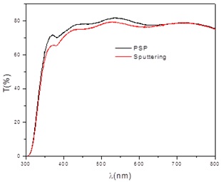
Figure 4 Transmittance spectra of TCO/SnO2 structures, where the buffer layer was deposited by PSP and by sputtering.
Comparing Figures 1 and 4 it is observed that the deposit of the buffer layers, both by PSP and by sputtering on the TCO, does not alter its transmittance, as a consequence of the thicknesses of the buffer layers, significantly lower than the TCO ones. A slight decrease in the thickness of the layers under thermal treatment was observed, probably due to a greater compactness of the grains and a loss of material under this treatment.
The morphological properties obtained from the AFM technique are shown in Figure 5. With the thermal annealing, the film particle of the sample deposited by PSP increases while an opposite process occurs for the sample deposited by sputtering, and the surface roughness was similar for both structures. The post-thermal treatment has a greater effect in reducing the roughness of the structure in the case of the SnO2 layer deposited by sputtering, respecting that deposited by PSP.
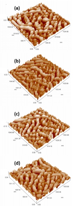
Figure 5 AFM images of samples of TCO/SnO2 structures: (a) as-grown PSP-SnO2; (b) annealed PSP-SnO2; (c) as-grown Sputtering-SnO2; and (d) annealed Sputtering-SnO2.
Finally, the calculated values of RT according with the equation (4) correspond to the measured ones. Table 3 summarizes the values of the shunt resistance, average transmittance, thickness, RMS roughness and Haacke’s modified figure of merit of the TCO/buffer structure.
Table 3 Sheet resistance (Rsh), average transmittance (Tave), thickness of TCO+SnO2 layer(d), RMS roughness (R) and Haacke’s modified figure of merit of the TCO/buffer bi-layers. (Only TCO and SnO2 annealed samples are presented according with the results shown in table II).
T-15/SnO2 conditions |
Rsh (Ω/sq) |
Tave (%) |
d(TCO+ SnO2) (nm) |
R (nm) |
(T10/Rsh)·1/R (Ω-1nm-1)×10-5 |
SnO2 by PSP |
14.1 |
72.9 |
376 |
2.1 |
107 |
SnO2 by Sputtering |
15.3 |
72.5 |
385 |
2.8 |
90 |
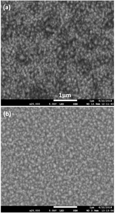
Figure 6 shows the top view SEM micrographs of the surfaces of the TCO/SnO2 bi-layers both with post- thermal annealing. A better uniformity is observed in the layer deposited by sputtering on T15 with a better contrast, according with the higher conductivity. Therefore, a better morphological property is obtained when the SnO2 layer is deposited on the conducting glass substrate T15 by sputtering technique.
Conclusions
Our results show that for photovoltaic applications, commercial conductive glass T15 is better TCO than T7. From the comparison of Tables 1 and 3, the use of the SnO2 as buffer layer improvement the TCO properties. Moreover, if the morphology is considered, the results of Table 3 show that both the PSP and sputtering techniques are appropriate for the deposition of SnO2 as buffer-layers in solar cells with superstrate structure. In reference [18] we show that, if a TCO presents a low morphological quality, the deposit of the buffer layer considerably improves the properties of the TCO and of the solar cells. In this work, we have shown that TCO with good optical, electrical and morphological properties, the deposition of a buffer layer does not produce significant changes in the properties of the TCO. In contrast, with the case of nonhomogeneous TCOs, with many pin-holes and/or high roughness. The results shown in this paper allow an assessment of the type of TCO to be used and its improvement in the processing of high efficiency solar cells in thin film technology.

