


 nova página do texto(beta)
 Inglês (pdf)
 Artigo em XML
 Referências do artigo
 Enviar este artigo por email
 Citado por SciELO
  Similares em
SciELO
Similares em
SciELO 
 Permalink
Introduction
Bismuth (Bi) is a versatile material to be laser processed in thin films. Laser-induced oxidation by CW and pulsed laser irradiation has been reported in Bi thin films by various research groups [1-4]. Additionally, laser-induced surface modification without oxidation has been studied by using laser pulses [5-6]. Recently, the LIPSS formation in Bi thin films grown by DC-sputtering technique was reported for the first time. Polycrystalline Bi thin films were obtained by the sputtering technique. To obtain LIPSS, laser irradiation experiments were done by using ns laser pulses [6]. It is well known that LIPSS formation is determined by the laser parameters such as: wavelength, laser pulses number, per-pulse laser fluence, laser polarization, pulse duration, among others [7].
To date, very little work has been done to investigate the influence of crystal orientation of the laser-processed material on the LIPSS features [8-10]. Recently, by using fs-laser pulses the effects of crystal orientation on the LIPSS formation have been investigated in silicon and nickel. Jiang et al. have demonstrated that the formation of laser-induced periodic surface structures (LIPSS) in silicon depends on the crystal orientation [8]. On the other hand, Seado et al. have found differences on the LIPSS formation in poly crystalline and oriented nickel samples [9]. This means that crystallographic orientation of a material must be taken into account as an important parameter, which affects the formation and orientation of LIPSS. From the best of knowledge, there is a lack of studies on the LIPSS formation on oriented thin films by using ns laser pulses.
There are many thin films deposition techniques to obtain crystallographically oriented thin films, as well as polycrystalline thin films. Deposition of Bi thin films has been reported by several methods such as thermal evaporation, DC and RF magnetron sputtering, molecular beam epitaxy [11], electron-beam evaporation and pulsed laser ablation. Recently, Rodil et al. published a comparative study of the growth of Bi thin films by various PVD techniques [12]. DC and RF sputtering, thermal and electron beam evaporation and pulsed laser deposition were used to deposit Bi films. They found that while by using electron-beam and thermal evaporation, which are low energy deposition techniques, oriented Bi thin films in the (003) direction are obtained; by employing sputtering techniques, polycrystalline Bi films are produced. On the other hand, by means of the PLD technique, crystallographic orientation of the films is dependent of the ion energy in the plasma. In this manner, while bismuth films grow on the (012) preferential orientation for ion energies about 270 eV, the (003) direction is obtained for ion energy values below 120 eV.
In the present work we study for the first time the effects of crystallographic orientation of Bi thin films on the LIPSS generation by using ns laser pulses at per pulse laser fluences below ablation threshold. With this purpose, polycrystalline and oriented thin films were deposited by using the PLD technique. Laser irradiation experiments to generate LIPSS on Bi thin films were carry out taking into account irradiation parameters reported elsewhere [6].
Experimental details
Deposition of bismuth thin films by PLD
For Bi films fabrication, a Nd:YAG laser (9 ns and 10 Hz repetition rate) was used. Ablation experiments were carry out at two different wavelengths: the fundamental line (1064 nm) and its second harmonic (532 nm). The laser beam was focused on a bismuth target (99.9 % purity) inside a vacuum chamber evacuated to a base pressure of 1×10⁻⁴ Pa. Figure 1 illustrates the experimental setup of the system used to deposit the Bi films. The ejected material during the ablation process is condensed and deposited on glass substrates (2 cm × 2 cm) placed in front of the rotated Bi target. The target-substrate distance was 6 cm. The plasma parameters (mean kinetic ion energy, Ek and plasma density, Np) were obtained using a Langmuir planar probe, located at the substrate position, and then removed after the plasma parameters were measured. Details about the acquisition of the plasma parameters were reported elsewhere [12]. The deposition conditions for each wavelength considered in this study are listed in Table 1. All deposits were made at room temperature and at the base pressure.

Table 1 Deposition parameters of Bi thin films by PLD.
Parameter |
Value |
|
Wavelength (nm) |
1064 |
532 |
Energy (mJ) |
22 |
11 |
Per pulse laser fluence (J/cm2) |
1.35 |
0.95 |
Target-substrate distance (cm) |
6 |
|
Deposition time (min) |
10 |
80 |
Deposition rate (nm/min) |
40 |
7.5 |
Maximum Ek(eV) |
40 |
70 |
Maximum Np (cm-3) |
1×10¹² |
8×10¹² |
Bi films characterization
The thickness of the Bi thin films was measured by profilometry (KLA Tencor D-120). Surface morphology of the films was analyzed with a scanning electron microscope (Jeol JSM6510 LV) and the structural characterization was determined by X-Ray diffraction (Bruker D8 Discover).
LIPSS formation
In order to generate LIPSS on the Bi films, a similar experimental setup reported in a previous work was used [6]. The laser used to irradiate the Bi thin films was the same utilized to perform ablation experiments. LIPSS were generated irradiating Bi thin films with the second harmonic emission line of the Nd-YAG laser (532 nm) and 1 Hz repetition rate. The per pulse laser fluence was set at 80 mJ/cm2 and 50 pulses were applied in each spot. The topography of the laser-irradiated zones were characterized by Atomic Force Microscopy using a Nanosurf easyscan 2 microscope, in the tapping mode.
Results and discussion
Figure 2 shows the thickness of two Bi thin films measured by profilometry. These two samples were deposited by using 1064 nm and 532 nm in the ablation experiment. In order to obtain similar thicknesses in the two thin films, the deposition time was varied (see table 1).

Figure 2 Thickness comparison for Bi thin films deposited with 532 nm and 1064 nm. Inset shows a photograph of thin film deposited with 532 nm.
In Figure 3 SEM micrographs corresponding to Bi thin films deposited with 532 and 1064 nm are showed. The micrograph 3a shows the surface of a Bi thin film deposited with λ=1064 nm at a per pulse laser fluence of 1.35 J/cm2. The thin film has droplets with diameters greater than 1 µm (splashing effect). The formation of drops has been observed in the majority of films deposited by PLD technique and in some cases this effect can be viewed as a disadvantage [13]. On the other hand, sub-micrometric particles constitutes the surface of the thin film. Figure 3b corresponds to a deposited thin film with λ = 532 nm at a per pulse laser fluence of 0.95 J/cm2. In this case, it is possible to observe a smoother surface, in which splashed particles exist in smaller proportion. It is clear from SEM micrographs that both, wavelength and the per pulse laser fluence play an important role in the surface quality of the Bi thin films.

The samples characterized by SEM were also analyzed by X-Ray diffraction. Figure 4a shows the X-ray diffraction patterns of a sample deposited with 1064 nm. The reflections (003), (012), (104), (110), (006), (202), (024) and (107) observed in the zoom of the diffractogram (see inset), indicate the polycrystalline nature of the Bi thin film deposited with 1064 nm. Taking into account the XRD card (00-005-0519) of bismuth, all the peaks correspond to polycrystalline pure bismuth. On the other hand, the XRD pattern of the sample deposited with 532 nm is shown in the Figure 4b. The diffractogram in Figure 4b contains only the family planes in the (00l) direction, indicating that the Bi thin films are textured. There are no additional diffraction peaks, as observed in the inset of Figure 4b. Crystallographic orientation of Bi thin films can be achieved by controlling the kinetic energy of plasma ions [12]. Rodil et al. reported crystallographic orientation of Bi films in two ion energy intervals 100-120 eV (low energy) and 260-280 eV (high energy). It is worth noting that in this work, crystallographic orientation is achieved at lower ion energy. An ion energy of 70 eV was obtained during laser ablation with 532 nm.
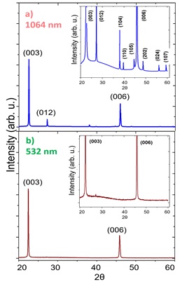
Figure 4 XRD patterns of bismuth films deposited with a) 1064 nm and b) 532nm. Insets shown magnified diffractograms images.
The AFM images of the laser treated zones are shown in the Figure 5. Both AFM micrographs have the same scale and there are six lines in each one. By using a wavelength of 532 nm, 50 pulses at a per pulse laser fluence of 80 mJ/cm2 is possible to generate LIPSS in the two types of Bi films. One can observe that perpendicular LIPSS respect to the laser beam polarization were obtained for the two types of Bi thin films, this is in good agreement to that reported previously in ref. [6]. The crystallographic orientation determines the features of ripples formation. At the top view, differences in the wide (crest and valley) and form of LIPSS can be observed. In the micrograph 5a ripples appear to be like wider curved segments. In contrast, LIPSS in micrograph 5b are almost linear parallel segments with thinner crests and wider valley. In both cases the LIPSS period is near to the irradiation wavelength (532 nm).
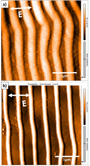
Figure 5 AFM micrographs of LIPSS generated on Bi thin films. a) Polycrystalline thin films and b) textured thin films
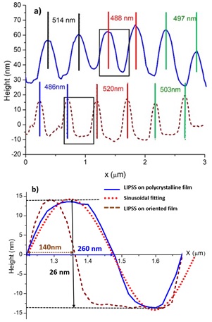
The LIPSS differences can also be identified by analyzing the LIPSS profile obtained from AFM micrographs. Figure 6 shows LIPSS profiles written on polycrystalline and textured Bi thin films. As it can be seen from Figure 6a the ripples period is near to the irradiation laser wavelength, giving in both cases a ripple separation average of around 500 nm ±10 nm. These type of LIPSS are called LSFL (Low Spatial Frequency LIPSS), because their period is near to laser wavelength and are obtained when ns laser pulses are used to perform the LIPSS [14]. In Figure 6b ripples profiles written on polycrystalline and textured Bi thin films are compared to stablish differences between them. In the first place, ripples on polycrystalline films have a sinusoidal-like form (blue dash-dot line). This is confirmed when a sinusoidal fitting y=14.3sin[π(x-763)/232], with parameters in nanometers and a correlation coefficient of 0.97 is applied to the ripple profile (red dotted line). It is clearly observed from Figure 6b, that ripple profile for textured thin films does not obey a sinusoidal-like form. In this case a rectangular-like valley characterizes the majority of LIPSS.
Conclusions
It has been shown that textured and polycrystalline thin films was successfully obtained by pulsed laser ablation when properly deposition parameters are used. Additionally, it has been demonstrated for the first time that crystallographic orientation of bismuth thin films determines some features of LIPSS written with ns laser pulses at a per pulse laser fluence below the ablation threshold. LIPSS were generated perpendicular to the laser polarization and the period of ripples was in the order of the irradiation wavelength, this is in good agreement with LIPSS recorded in sputtered Bi thin films previously reported. Some differences were identified in the features of ripples recorded on polycrystalline and textured Bi thin films. Further work is necessary with the aim to learn more about the crystal orientation influence on the LIPSS characteristics.

