


 nueva página del texto (beta)
 Inglés (pdf)
 Artículo en XML
 Referencias del artículo
 Enviar artículo por email
 Citado por SciELO
  Similares en
SciELO
Similares en
SciELO 
 Permalink
Introduction
Calorimeters are essential tools used to find thermodynamic properties (i.e. changes in enthalpy ΔH, Gibbs free energy ΔG, entropy ΔS and heat capacity ΔC p ) in a wide range of scientific fields such as chemical, biochemical, biology, biotechnology, pharmacology, and nanoscience [1-4]. Usually, microcalorimeters include a reaction chamber, a temperature sensor to measure the heat released or absorbed by the chemical reaction of the samples in the reaction chamber [4] and also include heaters for device calibration; moreover, differential microcalorimeters use an additional chamber as a reference chamber [5]. Some calorimeters use thermistors [6,7] or thermopiles [5,8-9] as thermal sensors, however, thermopiles have higher sensitivity than thermistors due to the absence of an electrical current [4]. Since thermopiles convert thermal energy into electrical, they have zero offset and the flicker noise could not affect static detection [10]. Besides, thermopiles do not require biasing; thus, there is no power dissipation neither interference caused by power supplies [13]. Thermopile’s differential temperature measurements reduce or even remove common-mode interferences such as room temperature fluctuation. In addition, thermopiles have been widely used as thermal vacuum sensor [14] and gas sensing [10,15-17]. In calorimeters, the thermal resistance of thermal sensor converts the heat released by an exothermic chemical reaction into a temperature gradient [17]. Therefore, the thermal resistance must be known to calculate analyte’s concentrations [5,8,17] to model a differential calorimeter and to optimize the thermopile design. Due to the complex geometry of thermal sensors, usually, thermal resistance is experimentally found. Nevertheless, thermal resistance is also obtained by Finite Element Method (FEM) [10,18], thermal sensor models are based on one-dimensional Fourier’s stationary heat equations, so these models frequently divide the thermal sensor in two [15,18] or three zones [10], and take into account radiative power [10,15] or heater power as heat source [18].
The present paper discusses three 3D finite element models analyzed in ANSYS to calculate the thermal resistance of the MEMS thermal sensor. We divided the thermal sensor into four zones, instead of two or three zones as in [10,15,18] and since we added an SU-8 layer, every zone had different thickness. The first model includes all sensor’s layers, the second model settled an equivalent thermal conductivity, and an equivalent thickness for each zone as in [10,15,18]. The third model offers a new approach to reduce the simulation time and to optimize the thermal sensor design parameters, thus besides an equivalent thermal conductivity we propose an equivalent thickness of same height for all zones. Also, we analyzed three different ways to apply or generate heat for the first model: on a surface [10,15,18], in volume, or applying an electrical current to the heater. As well as we consider different thermopile strip widths for the second and third models. This work also describes the thermoelectrical characterization of the thermal sensor to get the device performance parameters and explains some FEM models to find thermopile parameters such as temperature sensitivity and electrical resistance.
Operating principle
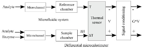
Figure 1 shows a MEMS differential thermal
sensor for analyte measurement (i. e. glucose), which consists of a microfluidic
system and a differential calorimeter. An infusion pump supplies analyte and
enzyme solutions by two different inlets to the microfluidic system, then both
solutions mix to each other through the microchannel, afterwards, the enzymatic
reaction takes place in the reaction chamber. Since the reference chamber holds
its temperature, the thermal sensor measures the temperature gradient and
generates an electrical potential which signal must be filtered and amplified
through a signal conditioning. An enzymatic reaction generates the heat
q proportionally to the reaction molar enthalpy
Heat flow dq/dt or thermal power ΔP is directly proportional to the product formation rate d[C P ]/dt or to the substrate consumed rate -d[C S ]/dt, also known as reaction rate constant or reaction rate coefficient k. When substrate concentration is consumed it has an exponential decay, so heat flow is
Sensor’s thermal resistance R
th
converts the thermal power of the enzymatic reaction to a temperature
gradient as
While thermal resistance is calculated as
Sensor’s performance is determined by several parameters such as device’s
responsivity [5,8] also known as heat power sensitivity [12,14] or thermopile’s electrical sensitivity [10]
Thermal noise is the main thermopile noise source which is given by
Thermal sensor design
The thermal sensor area is a structure of 10 mm×10 mm. Silicon substrate integrates a thermopile and two heaters as a single thermal sensor (Figure 2). The thermopile consists of 78 thin film n-type polysilicon and aluminum thermocouples. Heaters are of n-type polysilicon which can be used for device characterization, chambers temperature control or device calibration. The thermal sensor is over a thin membrane to minimize the sensor’s thermal mass and to reduce the time response [5]. A polymer layer is on top of the thermal sensors to obtain a smooth surface. The thermal sensor includes a small window around the thermopile junctions to preserve the heat nearby the thermopile junctions. Electrical connections are of aluminum.
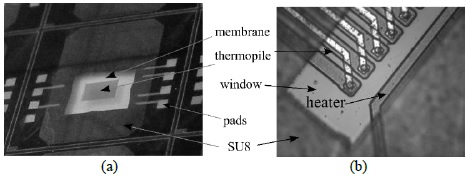
Figure 2 Thermal sensor images of a (a) macroscopic view and (b) hot junction and heater microscopic view.
We used a back side polished p-type wafer with <100> orientation, 100 mm diameter, 500 μm thickness and nominal resistivity 4-40 (-cm in a six-level manufacturing process. At zero level, we formed the membrane layer and back-side layer; a 50 nm SiO2 layer and a 300 nm Si3N4 layer constitute the membrane layer. At first level, we defined polysilicon strips (1.2 μm thickness). At second level, we created contacts definition and a 0.8 μm SiO2 layer for electrical isolation. The third level is metallization, so we added a 0.8 μm Al/Cu layer. At fourth level, we performed passivation etch of a 0.3 μm oxide layer and a 0.5 μm nitride layer. At fifth level, we defined back-side windows. Finally, at sixth level, we added a 25 μm SU-8 layer.
Thermal modeling
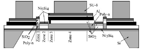
Figure 3 shows the thermal sensor cross-section view. Heater, membrane, insulation and passivation layer represent zone-1, where heater generates heat flux, q 0 . Zone-2 separates the heater and thermopile hot junctions, formed by membrane, insulation and passivation layers. Thermopile’s hot junctions form zone-3, which includes membrane, insulation and passivation layers and thermal elements (n-polySi/Al). Zone-3 layers and an additional SU-8 layer form zone-4. Because of symmetry we only considered the half-length heater, so zone-1 length is 3 μm, zones 2, 3 and 4 have 22 μm, 27 μm and 1944 μm lengths, respectively. Additionally, we defined a width of 1372 μm for all zones, so, we only use length l n and thickness d n , as zone dimensions, where n stands for zone number.
In order to find the sensor’s thermal resistance, we developed three different
models for ANSYS simulations, named ANSYS-TC, ANSYS-4Z, and ANSYS-ME. In
ANSYS-TC model we included all material’s layers. In ANSYS-4Z model we
calculated an equivalent thermal conductivity and equivalent thickness for each
zone. In ANSYS-ME model we calculated an equivalent thermal conductivity and set
up an equivalent thickness where all zones had the same height. The boundary
conditions for all models are ambient temperature of 300 K and air convection
coefficient
Subscript j relates each material layer, wj is the coverage coefficient [12] defined by the material layer and zone width ratios. We applied a heat flow, q0, on the zone-1 lateral surface. Also, we analyzed two different conditions, by using the same width for all layers (ANSYS-4ZwT model) and a different width for the thermopile strips (ANSYS-4ZwTp model). For the ANSYS-ME model we specified the same thickness to all zones, so we settled a new equivalent thickness and a new equivalent thermal conductivity, our innovation. Like ANSYS-4Z model we analyzed two different conditions, the same layer width (ANSYS-MEwT model) and a different width for the thermopile strips (ANSYS-MEwTp model).
Experimental details
Thermoelectrical Characterization
For this work we characterized five chips, labeled A, B, C, D, and E; since only chip D was wire bonding, we tested the other chips using probe station tips. We used an Agilent E3645 power supply and an Agilent 34411A multimeter for electrical resistance measurement of chips A, B, and C. To characterize the chip D, we used a portable infrared camera Fluke( Ti25, an InfiniiVision DSO-X 3054A oscilloscope and an Agilent E3631 power supply. To obtain the electrical resistance of the heather and thermopile of chip D, we applied a voltage range from -5 V to +5 V, with 1 V steps. We got the electrical resistance by the slope of the regression line. By using the four-wire resistance measurement technique, we found the heater and thermopile electrical resistance of chips A, B, C, and E. To obtain the thermal sensor’s heat power and temperature sensitivities we used a joule heating experiment, where a CC source drives the heater next to the hot junction. We only obtained thermopile’s sensitivity for chip D. We applied a voltage range from 2 V to 10 V with 0.5 V steps to the heater, then we measured the temperature with an infrared camera and the thermopile’s voltage using the oscilloscope to obtain device responsivity. In addition to the ANSYS models we described before, we simulated the thermopile to get its electrical resistance and sensitivity, considering two thermopile’s materials.
From literature we got the Seebeck coefficient of -200 µV/K and -1.7 µV/K for n-type polysilicon [21] and aluminum [22], respectively; as well as other material properties such as thermal conductivity, mass density and heat capacity [21]. To obtain the electrical resistance of heather and thermopile we supplied an electrical current of 100 µA to each of them, and we calculated the output voltage according to Ohm’s Law. To get thermopile sensitivity we applied a temperature difference of 100 mK to the hot and cold thermopile’s junctions to measure the thermopile’s output voltage.
Results and discussion
Electrical resistance
We calculated the thermocouple’s electrical resistance of 2.7 kΩ based on its geometry considering an electrical resistivity of 0.032 µΩ·m [22] and 16 µΩ·m [21] of aluminum and n-type polysilicon, respectively, thus the thermopile’s electrical resistance was 209.3 kΩ. Heater’s electrical resistance was 3.5 kΩ considering n-type polysilicon, 6 µm width, 8 µm thickness and 1590 µm length. Since electrical connections are of aluminum we discarded its resistance. Due to thermopile’s complex geometry and our limited computational resources we only could simulate a maximum of 70 thermocouples in ANSYS; therefore, to confirm thermopile’s linearity, we carried out simulations using 1, 10, 30 and 70 thermocouples. In ANSYS we obtained a thermocouple’s electrical resistance of 2.7 kΩ, so thermopile’s electrical resistance was 209.2 kΩ, yielding an error of 0.05% compared to the calculated value. The average electrical resistance we measured was 221.4 kΩ with a standard deviation of 5.5 kΩ, thus the relative error was 5.7%. The heater’s electrical resistance measured was 3.6 kΩ, so the relative error was 0.1%.
Temperature sensitivity
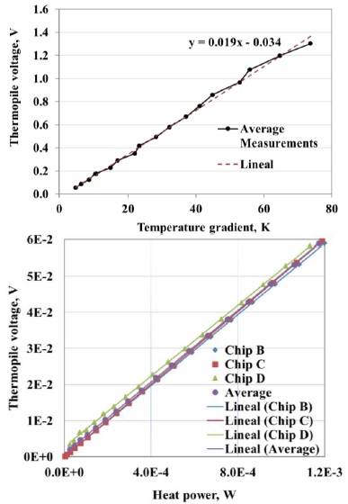
Seebeck coefficient of one thermocouple was 198.3 μV/K, so the calculated thermopile sensitivity was 15.47 mV/K. To experimentally obtain the temperature sensitivity of chip D, we performed three tests, so we got the thermopile’s sensitivity average by the slope of the regression line, which was 18.98 mV/K (Figure 4a), with a relative error of 18.5%. We completed ANSYS thermoelectric analysis using only 70 thermocouples because of thermopile complex geometry and limited computational resources. Nevertheless, Seebeck coefficient is a mass property and has no shape dependency, thus if we reduce thermocouple’s length, its sensitivity remains the same. Therefore, we performed ANSYS simulations for 60 thermocouples of different strip lengths of 1993 μm, 997 μm and 498 μm, getting the same temperature sensitivity of 15.469 mV/K, yielding a 0.01% relative error to the calculated value, also reducing the simulation time from 48 hours, 16 hours to less than 2 hours, respectively.
Heat power sensitivity
Figure 4b shows heat power vs thermopile output voltage for chips B, C, and D, by the slope of the regression line, we found values of 49.3 V/W, 50.2 V/W and 49 V/W, respectively. We also tested a chip without the hole under the thermopile and we got a responsivity of 0.1 V/W, proving that substrate thermal mass reduces the heat power sensitivity.
Thermal resistance
To find the thermal resistance we supplied to the heater of chip D a voltage
range of 2-10 V with 1 V steps and measured the temperature gradient by an
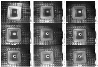
infrared camera; figure 5 depicts the
chip D thermal map, to point out the heater temperature rising we used the
same temperature scale. Figure 6 shows
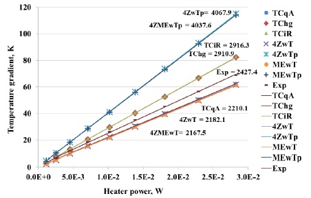
the Chip D thermal resistance by the slope of the regression line plotting
heater power vs temperature gradient, so finding a thermal
resistance of 2427 K/W. Furthermore, we calculated an average thermal
resistance of
ANSYS models
In [10,15,18] used 2-D models to analyze thermal sensors, instead we managed 3-D ANSYS elements to apply an electrical current. In ANSYS-TCqA model, we supplied the heat power to the lateral area of zone 1, finding a thermal resistance of 2210 K/W with a 9% of relative error, which is the lowest error of all models. For ANSYS-TChg and ANSYS-TCiR models the heater volume generated the heat power, showing an analogous behavior, with thermal resistance values of 2911 K/W (TChg) and 2916 K/W (TCiR), respectively, with a relative error of 20%. In ANSYS-4Z models we calculated an equivalent thermal conductivity and an equivalent thickness for each zone as in [10,15,18]. Besides, we considered two different thermopile width dimensions: the same for all layers (ANSYS-4ZwT model) and a different thermopile strips width (ANSYS-4ZwTp model). As a result, we found that the ANSYS-4ZwTp model thermal resistance almost doubled the ANSYS-4ZwT model, 4068 K/W, and 2181 K/W, respectively. Since thermal resistance is inversely proportional to cross-section area where heat transfer takes place if we shorten the thermopile width strips, then the thermal resistance increases. The proposed ANSYS-ME model, besides an equivalent thermal conductivity, defines the same height for all zones specifying a new equivalent thickness. As in ANSYS-4Z models, we analyzed the same conditions considering different widths. Table 1 shows equivalent thermal conductivities of four zones used in ANSYS-4Z and ANSYS-ME models. We used an equivalent thickness of 3.15 μm for ANSYS-ME model. The ANSYS-MEwTp model thermal resistance almost doubled the ANSYS-MEwT model, 4038 K/W, and 2168 K/W, respectively, as in ANSYS-4Z models. ANSYS-TCqA, ANSYS-4ZwT, and ANSYS-MEwT models had the lowest relative error 9%, 10% and 11%, respectively. As a result, heat transfer analysis on the proposed model simplifies complex geometries and reduces simulation time. Besides, we could use 2D elements because these models do not need a 3D heater for heat transfer. ANSYS-TChg and ANSYS-TCiR models had a responsivity of 45 V/W and a 9% relative error. ANSYS-TCqA, ANSYS-4ZwT and ANSYS-MEwT models had a responsivity of 43 V/W, 34 V/W and 33 V/W, with a relative error of 31%, 32% and 32%, respectively. Since responsivity is directly related to thermal resistance, ANSYS-4ZwTp and ANSYS-MEwTp models responsivity almost doubled the ANSYS-4ZwT, and ANSYS-MEwT models, 63 V/W and 62 V/W, respectively; reducing the relative error to 27% and 26%, respectively. Table 2 summarize thermal resistance and responsivity obtained from ANSYS models.
Table 1 Zone’s equivalent thermal conductivity [W/mK] used in ANSYS models.
Zone |
4ZwT |
4ZwTp |
MEwT |
MEwTp |
1 |
21.1 |
21.1 |
21.1 |
21.1 |
2 |
10.7 |
10.7 |
6.6 |
6.6 |
3 |
64.4 |
28.1 |
80.8 |
35.2 |
4 |
9.1 |
4.1 |
83.2 |
37.6 |
Thermal sensor parameters
Table 3 summarizes the thermal sensor parameters. Since ANSYS-MEwT model is our innovation, we compared it to measured values. The lowest temperature gradient that the thermal sensor can measure is 3.2 μK. The least power gradient that the thermal sensor can detect is 1.2 nW. For a temperature gradient of 10 mK, it has a high SNR of 3134. The device resolution bandwidth was 2 nW, which is lower than literature [8,11]. The thermal noise over 1 Hz was 60 nV which is close to previous reports [5,18,13]. In general, thermal sensors used as calorimetric biosensors have less than 10 V/W device responsivities [5,8-9,11,23], because all of them include their microfluidic system for device calibration. On the other hand, IR sensors have higher responsivities as 70 V/W [10], because they considered the air during simulation or experimental measurements. Based on the Seebeck coefficients from the literature we found an 18% relative error for thermopile sensitivity. Since we used the same material properties thermopile electrical resistance obtained by ANSYS and the calculated value were similar.
Table 3 Thermal sensor parameters.
Parameter |
Calculated |
Measured |
Relative error, % |
Thermopile electrical resistance (kΩ) |
209 |
221 |
6 |
Heater electrical resistance (kΩ) |
3.533 |
3.536 |
0.1 |
Thermopile sensitivity (μV/K) |
15 |
19 |
18 |
|
Thermal resistance (K/W) (ANSYS-MEwT model) |
2167 |
2427 |
11 |
|
Responsivity (V/W) (ANSYS-MEwT model) |
33 |
50 |
32 |
|
Thermal noise, (1 Hz)
|
59 |
60 |
3 |
NETD (μK) |
3.8 |
3.2 |
18 |
|
NEP (nW) (ANSYS-MEwT model) |
2 |
1 |
43 |
D
|
57 |
81 |
30 |
SNR ( |
2626 |
3134 |
16 |


Conclusions
We proved that finite element analysis simplifies the operations to get the thermal sensor parameters. Since the aspect ratio of thermopiles needs many nodes to solve, so we proposed to define zones for different layers of material to replace the exact geometry and to define the same height to all zones, to get an equivalent thermal conductivity and an equivalent thickness. Though we got an error of 11% for thermal resistance, we developed a new way to simplify the finite element analysis that we can use to evaluate the design of calorimeters. However, the electrical resistance needs considering the whole thermopile using 3-D thermoelectrical elements. Thermopile linearity allows reducing simulation time by decreasing the number of thermocouples. Likewise, we may get thermocouple’s sensitivity in less time by shortening the thermocouple lengths. Once we experimentally measured heater’s electrical resistance we also got it by finite element analysis, choosing from literature the material properties that yield the lowest error. Finally, parameters such as thermal noise and resolution guarantee that we could use the thermal sensor for glucose measurement. Though, if the thermal sensor includes the microfluidic system the device performance changes.

