


 nova página do texto(beta)
 Inglês (pdf)
 Artigo em XML
 Referências do artigo
 Enviar este artigo por email
 Citado por SciELO
  Similares em
SciELO
Similares em
SciELO 
 Permalink
Introduction
Zinc doped tin oxide thin film semiconductor improves its mechanical properties, suitable for different technology applications. Doped tin oxide is used for solar cells [1], gas sensor [2], photo catalysis [3], pollutants detection [4], anode for ion lithium batteries [5] as quantum dots [6,7], ferromagnetic [8] and photoconductive devices. Nowadays, Zn doped SnO2 show promising applications for high temperature semiconductor [9] and optoelectronics devices [10], both properties are being improved by tuning the amount and type of dopants. In solar energy research, Zn doped SnO2 nanoparticles (NPs) are being used as photo anode material to induce negative shift in the flat-band potential to increase the isoelectric point in dye-sensitized solar cell [11]. Doped tin oxide as thin films show high optical transparency and good electrical conductivity for optoelectronic applications [12], then it is significant to determine its growing, structure, elastic deformation and resistance to permanent deformation. When the mechanical properties (MPs) are known, it can be used effectively in electrochemical, photoconductive devices, transparent conductive oxide electrodes for thin film solar cells and other devices. The mechanical indentation has been the most commonly used technique to measure the MPs of materials due to the easy data acquisition. This traditional indentation test consist in acquiring the optical image of the indent and taking the measurements from it. This method, clearly imposes a lower limit on the deep scale of the indentation test. During the past two decades, the scope of indentation testing has been extended to the nanometer range. This has been achieved mainly through the development of adequate instrumentation with the capacity to measure simultaneously the load and displacement during the indentation process [13,14]. In recent years, the MPs (elastic modulus, hardness, stiffness, and resistance to permanent deformation) study of materials on the nanoscale has expected attention due to these properties, which are dependent on the size [15,16]. These studies have motivated the development of nano-composites and their technology application as thin films, useful for miniaturization the electronic components and for generation of new technologies [17]. On the other hand, a recently developed technique to measure MPs are the continuous stiffness measurement (CSM) method [18], it offers a significant improvement in the thin film nano-indentation testing, this technique gives good accuracy to determine the values and it was used to study our samples.
Several techniques have been employed to synthesize tin oxide based coatings such as sol-gel [19], radio frequency reactive magnetron sputtering [20], chemical vapor deposition [21] and its variants as spray pyrolysis (SP) [22,23]. Among these techniques, SP has proved to be easy, reproducible and technically a good way for adding dopant elements, it has high grown rate and cheap method to mass production of uniform large-scale area coatings, which is desirable for industry and solar cell production. As regards to the dopant presence, by SP is possible to obtain doped and textured thin films growth, then evaluate mechanical properties of the material.
In this report, the aim is to investigate the influence of the Zn dopant concentration on the growing characteristics; surface morphology and microstructure of SnO2 thin films, with exhaustive structural characterization using Rietveld refinement method to process the XRD patterns and correlate with mechanical properties. The studied samples were obtained by SP technique due to the advantages mentioned above.
Experimental details
Highly textured Zn doped SnO2 thin films were synthesized by SP technique; the methodology has been fully described before [24,25]. In summary, we have used a SP system including a mobile platform that provides an oscillatory movement to the spray nozzle. The starting solution was a dilution of tin tetrachloride (0.05M) in methanol. Zinc acetate was used as a dopant source and the atomic ratio between Zn and Sn was varied from 1 up to 33 at%. Corning 7059 (2.5 × 7.5 cm2) glass slides were used as substrate, the synthesis temperature was fixed at 773 ( 5 K. Micro-filtered air was used as a carrier gas; their pressure and flux were kept at 310 kPa and 4 L/min, respectively. The deposition process was intermittent, one sweep movement was spraying dissolution and two without spraying; the effective deposition time was around 4 min in order to get the same thickness among the samples. Table 1 shows the main synthesis parameters values and characteristics for the samples under study.
Table 1 Films synthesis parameters and characteristics. Rietvel refinement results.
Samples |
Zn/Sn in solution |
Zn/Sn in film by EDS |
Agglomerate Size |
Film thickness |
Growth rate |
Results from XRD with Rietvel Refinement |
|||||||
|
Lattice parameters |
a/c ratio |
Domain size by Rietveld |
Domain size by IBF |
Texture direction |
Weight |
Marchs´ parameter |
|||||||
(at%) |
(nm) |
(nm) |
(nm/s) |
a (nm) |
c (nm) |
(nm) |
(hkl) |
(%) |
G1 |
||||
JCPDS |
0.4738 |
0.3187 |
1.486 |
||||||||||
ZN01 |
0.0 |
0 |
323 |
325 |
85 |
0.4729 |
0.3177 |
1.489 |
32 |
35 |
(110) |
33 |
0.425 |
(100) |
33 |
0.426 |
|||||||||||
(211) |
33 |
0.273 |
|||||||||||
ZN02 |
1.0 |
272 |
467 |
121 |
0.4727 |
0.3177 |
1.488 |
25 |
33 |
(200) |
93 |
0.350 |
|
(101) |
7 |
0.334 |
|||||||||||
ZN03 |
2.9 |
191 |
439 |
114 |
0.4746 |
0.3181 |
1.492 |
16 |
23 |
(200) |
55 |
0.288 |
|
(101) |
45 |
0.357 |
|||||||||||
ZN04 |
4.8 |
204 |
390 |
101 |
0.4744 |
0.3175 |
1.494 |
16 |
20 |
(200) |
51 |
0.319 |
|
(101) |
49 |
0.394 |
|||||||||||
ZN05 |
6.5 |
244 |
310 |
85 |
0.4733 |
0.3172 |
1.492 |
16 |
21 |
(200) |
59 |
0.328 |
|
(101) |
41 |
0.381 |
|||||||||||
ZN06 |
9.1 |
208 |
337 |
88 |
0.4743 |
0.3178 |
1.492 |
16 |
21 |
(200) |
44 |
0.328 |
|
(101) |
56 |
0.398 |
|||||||||||
ZN07 |
23.8 |
0.5 |
156 |
274 |
71 |
0.4734 |
0.3167 |
1.495 |
12 |
16 |
(200) |
3 |
0.273 |
(101) |
97 |
0.492 |
|||||||||||
ZN08 |
33.3 |
1 |
154 |
244 |
63 |
0.4703 |
0.3166 |
1.485 |
13 |
19 |
(200) |
8 |
0.316 |
(101) |
92 |
0.458 |
|||||||||||
ND: Not Detected by EDS; JCPDS for reference values. Dopant concentration at% Zn/Sn in solution and in film; Agglomerate size; Film thickness and Growth rate. Rietvel refinement results: Lattice parameters a, c, a/c Ratio; Domain size (by refinement and from intensity broadening fit (IBF)); Texture directions used in Rietveld analysis with their respective weight percentage and first Marchs’ parameters values.
The thickness of the films were determined from near normal reflectance spectrum, acquired by Filmetrix F-20UV reflectance spectrophotometer. Surface morphology of the films were analysed by Field Emission Scanning Electron Microscopy (FESEM) model JEOL JSM-7401F and the microstructure was studied by analytical Transmission Electron Microscopy (TEM) using Philips CM-200 and JEOL JEM-2200FS instruments, the images were acquired in TEM and STEM modes. For TEM study, samples were made by two methods: first one the sample was scratch and immersed in 5% content of flourhydric acid in water, then it was floating directly the film from the glass slide by tension superficial in water and mounted it on a copper grid, and the second one was made using Focus Ion Beam (FIB) milling to study thin films cross section. The FIB equipment to make the sample was Jeol JEM-9320FIB with Ga ion source. The chemical composition of the films were found by X-ray photoelectron spectroscopy (XPS), Escalab 250Xi spectrometer and by X-ray energy dispersive spectroscopy (EDS), attached to both SEM and TEM microscopes. Raman spectra were acquired using a LabRam HR Vis-633 Horiba Micro Raman spectrometer with He-Ne Laser emitting at 632.8 nm. The spectra was acquired from 3 zones and the resultant intensity values were average, the exposure time for each one was 5 min, the microscope objective was 100× and grating was 1800 groves/mm. The atomic force images were acquired by Veeco SPM MultiMode IV working in tapping mode. Nano MPs such as hardness (H) and elastic modulus (E) of the samples were measured by nano-indentation technique using continuous stiffness measurement (CSM) method, by Nano Indenter G200 coupled with a DCM II head. The instrument was calibrated using a standard fused silica sample to find area function constants, being C0 = 24.05, C1 = -186.33, C2 = 6422.20, C3 = -26452.23 and C5 = 18012.30. The calibration of the equipment is very important due to the damage or worn of the Berkovich diamond tip, which can affect the area in which it functions the contact penetration depth h c , A(h c ) [26]. The area function has the following polynomial equation:
The area function for a perfect Berkovich indenter is given by
We use Berkovich diamond indenter with a tip radius of 20 ±5 nm, depth limit of 140 nm and strain rate of 0.05 s−1. The harmonic displacement and frequency was 1 nm and 75 Hz passion’s coefficient of ν = 0.22, respectively. Residual indentation of samples was recorded by AFM Nano Vision system attached to the instrument.
Crystal structure of the materials was evaluated by X-ray diffraction (XRD) in Bragg-Brentano geometry using a Philips X-Pert diffractometer; the patterns were acquired with 40 kV and 30 mA, using Cu K( ((=0.15418 nm) radiation and the scanning angle 2( varied between 20° and 80°, with 0.015° step. Lattice parameters, crystallite sizes, micro strain and preferential growth orientation were obtained through the Rietveld refinement method [27]. The refinement of XRD patterns were performed through the free software Fullprof, the criteria and sequence of refinement was achieved following the method proposed by Fuentes [28]. The starting structural model for SnO2 refinement was built with crystallographic data reported in Inorganic Crystal Structure Database 2004.
Results and discussion
Composition and growth rate
Zinc atomic percentage content in the starting solution and films are listed in Table 1. The dopant concentration in the synthesized materials do not correspond to the same amount in the precursor dilution. Although the dopant do not totally enter into the film but it has strong influence on the growth characteristics and its MPs. The Zn atoms amount in the films were lower than the detection limit by EDS, for the samples ZN02 up to ZN06 (until 9.1 Zn/Sn at% in dilution). In the case of the films obtained with higher Zn content in dilution, it was possible to detect by EDS and it was reported in the Table 1. In the rest of this work, the dopant percentage is referred to the start dilution amount, if not stated otherwise. The thickness growth rate was also influenced by the dopant concentration in the start dilution. First, it was perceived an important increase on the growth rate (44 %) for the sample with 1 at% of Zn/Sn in relation to the undoped sample. Then the growth rate decreased systematically as the Zn content increased in the precursor dilution (see Table 1). The Zn quantity content and grown rate changes on the films could be due to changes in the precursor dilution properties, since the pH changes slightly with the Zn amount content, this type of behavior was also reported by Bilgin et al. [29].
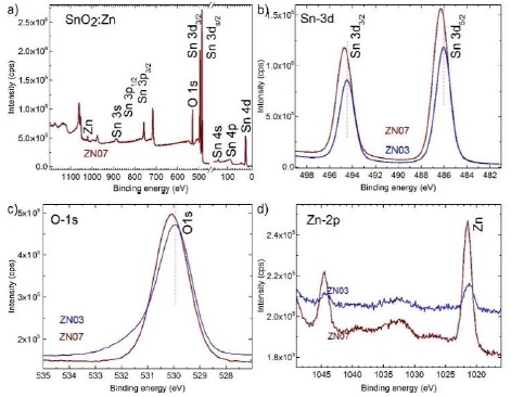
With the purpose to find Zn as a dopant in the SnO2 films, a couple of samples have been analyzed by XPS technique. Figure 1 shows the core level high resolution XPS spectra of Sn-3d, O-1s and Zn-2p for 2.9 and 23.8 at% of Zn/Sn (ZN03 and ZN07) samples. Figure 1a shows the binding energies of the sample, confirming the presence of tin, oxygen and dopant Zn. Figure 1b shows in detail, the binding energy of Sn 3d5/2 and 3d3/2 peaks with spin orbit separation of 8.42 eV, which are localized at 486.06 and 494.48 eV for 2.9 at% of Zn/Sn (sample ZN03); this binding energy of Sn 3d corresponds to Sn+4 ion (oxidative state). Although, the values reported by NIST XPS database for 3d5/2 and 3d3/2 are 486.6 and 494.50 eV, respectively; our measurement values are close. Comparing the binding energy values for Sn 3d5/2 and 3d3/2 intensities, for 2.9 and 23.8 at% of Zn/Sn content samples, there is a 0.24 eV shift toward upper energy for high Zn content sample (ZN07). This binding energy variation of Sn-3d core level with Zn doping can be qualitatively attributed to the formation of Zn-O-Sn bond. The electronegativity of Zn (1.65) is less than of Sn (1.96) and the electrons density around Zn atom in Zn-O-Sn bond is lower than that in Sn-O-Sn bond, which causes the upward shift of the Sn-3d core level energy. Figure 1c shows the O-1s transition peak and also an upward shift from 529.93 to 530.07 eV for the sample with high Zn content, it is another consequence of the Zn-O-Sn bond formation, The energy values is according to reported literature and do not belongs to ZnO, it belongs to O K level binding. Figure 1d shows the binding energy of the Zn 2p3/2 and Zn 2p1/2 transition intensities, which confirms the presence of Zn dopant in the SnO2 films, the relative intensity change shows the Zn amount contents qualitatively. Due to these results it could be concluded that the Zn dopant was incorporated by substitution to Sn atoms into the SnO2 lattice to form Zn-O-Sn bonds.
Structure and texture results
Figure 2a shows the X-ray diffraction patterns, the signal for undoped sample has different intensities and for doped films they changes systematically. It can be noticed a systematic change of patterns intensities, starting strong intensity from (200) toward (101) direction for low and high Zn dopant amount content samples, respectively. All patterns show polycrystalline structure and they index with JCPDS card number 41-1445, it was not detected other phases corresponding to zinc oxide or to new tin-zinc compounds. Taking the pattern intensities for undoped SnO2 as reference, the Zn doped SnO2 films present changes according to the Zn dopant content increase. These results indicate that doped films grew with systematic preferential orientation, according to the Zn content. In addition, the pattern intensities decreases and its wide increases; then the crystallinity of films decreases systematically as the Zn concentration increases. Table 1 shows the summary of the principal parameters obtained from Rietveld refinement for all films analyzed in this work. Figure 2b shows a typical example of the Rietveld refinement methodology results for each XRD patterns, this figure in particular represents the refinement for 2.9 at% Zn/Sn (sample ZN03).
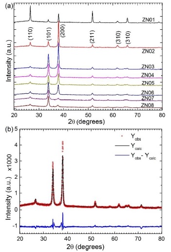
Figure 2 X-Ray diffraction patterns for (a) Zn-doped SnO2 thin films and (b) typical Rietvel refinement spectra for 2.9 at% of Zn/Sn.
The lattice parameters of SnO2 changes slightly as a function of Zn amount content, these values have been obtained from Rietveld refinement (Table 1). Figure 3 shows the lattice parameters difference in comparison with values reported in JCPDS card 41-1445. It can be noticed that the lattice parameter “a” and “c” for films with Zn dopants start increase in order of two thousandth for films contents up to 2.9 at% Zn/Sn and then for higher Zn dopant contents decrease systematically; this change could be due to the unit cell growth orientation relative to the substrate, due to the Zn atom binding (Zn-O-Sn). Therefore, for all films with the exception of ZN08 (33.3 at%) sample, the ratio a/c was less than that of the reference diffraction file; it showed the trend to increase with the Zn content (see Table 1 and Figure 3).
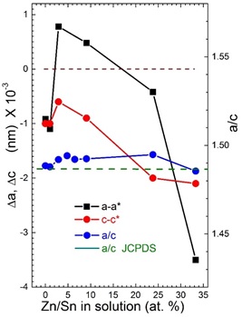
Figure 3 Lattice parameters difference (a-a* and c-c*) as a function of Zn contents. a*=0.47382 nm and c*= 0.31871 nm belongs to JCPDS 41-1445. It is include the a/c ratio variation.
Moreover, we have also obtained the domain size, as a function of Zn amount contents. The average size decreases generally starting from 32 nm for undoped up to 12 nm for 23.8 at% Zn/Sn doped material. These values were determined from the XRD pattern intensity broadening fit (IBF) using the Scherrer equation [23], it was calculated for each most strong diffraction intensities, respectively; the tendency of these values is consistent with that domain size obtained by Rietveld method, as the Table 1 shows. Another remarkable result obtained was the preferred growth orientation of the films, similar to indium doped zinc oxide thin film [22] reported previously. In brief, the Rietveld method calculate diffraction intensities as a function of Bragg reflection angle, Lorentz polarization factors, structure factor, intensity profile function, absorption factor and preferred orientation function or denominate pole density distribution Pg. The Fullprof program could consider as two or three phases of the same compound (same lattice parameters with different texture), using this option was refined the XRD (see Table 1 texture directions and their weight percentages). The Pg was evaluate using March-Dollase function (see Table 1 Marchs’ parameter values), the preferred grown of each studied film was determined evaluating this function, for every texture, then each one was weighted with their percentage; more details in [22]. This semi-quantitative evaluation of the inverse pole figure (IPF), in the normal direction to the substrate surface, was achieved for all observed intensities in the XRD patterns. The IPF determination for (200) intensity, initially increases abruptly for samples up to 6.5 at% Zn/Sn content, then it changed to (101) intensity from samples with 9.1 to 33.3 at% Zn/Sn contents systematically. Figure 4 shows the IPF calculated values for studied samples, the (200) and (101) d-space have a marked tendency to grown parallel to the substrate surface. Therefore, Zn dopant concentration generate changes in the SnO2 films growth orientation, in the (200) or (101) direction. These findings indicate that for higher Zn dopant presence in the started solution modifies the growth direction of the resulting SnO2 material by decelerating slightly the thickness growth rate, decreasing the particles agglomeration and domain size. The SnO2 film thickness growth rate in (200) direction is faster than (101), this is due to the properties changes of the start solution due to the Zn acetate salt quantity contents for doping purpose; the other reason, is the Sn and O atoms rate addition on the (200) and (101) SnO2 surface layer, it could be different due the atomistic affinity. The SnO2 mass densification is in the (200) direction and it is the preferred growth than others intensities by SP technique, being the optimum growing rate at 1 at% Zn/Sn amount content.
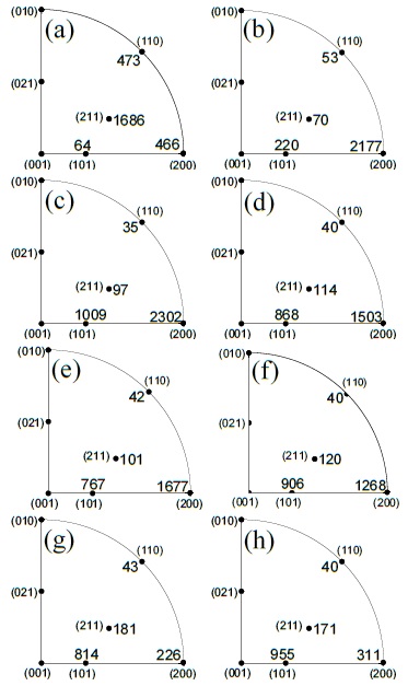
Figure 4 Inverse pole figure for Zn doped SnO2 thin films: (a) undoped, (b) 1, (c) 2.9, (d) 4.8, (e) 6.5, (f) 9.1, (g) 23.8 and (h) 33.3 at% Zn/Sn.
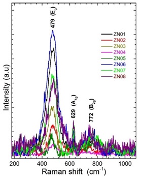
A complementary study about the structure was made by Raman spectroscopy. The spectra for all studied films have similar behavior such as shown in Figure 5. They show the presence of three characteristic vibration bands located at 479, 629 and 772 cm-1 which belongs to Eg, A1g and B2g vibrational modes for SnO2 rutile structure, respectively [30]. Our values is slightly shifted toward the left around 3 cm-1 respect to the reference, it is probably due to the dopant presence. It was do not notice the vibration modes of ZnO for any concentration. The Eg and B2g bands represent the vibration modes with displacement in the direction of the c-axis, A1g show the vibrations with displacements perpendicular to the c-axis and B2g represents asymmetric Sn-O stretching of SnO2. The signals for thin films show strong and wide intensity of Eg band but when the material is powder type show a strong intensity for A1g vibration mode [31]. The Eg vibration intensity decrease for high Zn at% of Zn/Sn, this widening of the intensity shape is due to the nanometric domain size, due to the phonon confinement. These variations in the intensities and shape is another evidence about the presence of Zn as a dopant in the SnO2 films.
Morphology and microstructure
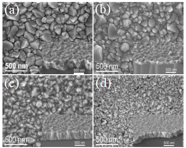
Thin films surface morphology was studied by SEM and AFM but the particle microstructure, shape and cross sectional evolution was studied by TEM. Figure 6 shows SEM images acquired with secondary electrons for different Zn percentages contents samples: (a) undoped; (b) 1; (c) 4.8 and (d) 33.3 at% Zn/Sn. For each one, it was included inset cross section image, both images show in detail the thickness growth and crystals agglomeration. It can be noticed that the film’s microstructure has been influenced by Zn dopant content. Figure 6a shows image from undoped film, the particle agglomerate average size is around 323 nm, this film does not present any noticeable texture, as determine by XRD pattern (Figure 2a). Figure 6b shows the image for sample with 1 at% Zn/Sn, it can be seen a similar morphology than undoped sample but with diminished particle agglomerate average size around 272 nm, this sample has a marked (200) preferential growth orientation, parallel to the substrate. Figure 6c shows the morphology of the sample with 4.8 at% Zn/Sn, it could be see the particle agglomerates size are homogeneous, with average size approximately 204 nm, this sample has a slightly preferential growth in the (101) direction and it starts to change from (200) growth direction. Figure 6d shows the morphology of sample with 33.3 at% Zn/Sn, it can be noticed that the particle agglomerate size decreased to around 154 nm and in this case the preferential growth changed completely to (101) growth direction parallel to the substrate. It is worthwhile to mention that the apparent discrepancy between agglomerate size observed by SEM and the crystallite size determined by the Rietveld method, could be clarified by the fact that X-ray diffraction calculate the mean domain size (crystalline particle) perpendicular to the diffracting plane, i.e. in the normal direction to the substrate surface (in Bragg-Brentano geometry). Instead, in image analysis by SEM we observe the particle agglomerate size (conglomerate domain) projected on the substrate surface. SEM micrographs showed that the particle agglomerate morphology was similar for all the samples, only average size decreased as the percentage of Zn amount dopant increase. The Table 1 shows the agglomerate size and domain size values, both decrease when the Zn dopant quantity increase in SnO2 films.
Thin films roughness was studied by AFM according to the dopant percentage, images are shown in Figure 7. The particle size and the flatness of the surface, decrease according to the Zn dopants content; the top and down distance in these images decrease systematically by the dopants amount increase in the samples. The images shown in Figures. 7a, Figures. 7b, Figures. 7c, Figures. 7d, Figures. 7e and Figures. 7f which are from 0, 1, 4.8, 6.5, 23.8 and 33.3 at% Zn/Sn dopants contents, respectively. The surface roughness values determined by root mean square (RMS) methodology were included in Table 2, these values decrease with the Zn dopant presence, systematically. The roughness for films with higher Zn dopant percentage content is less than for undoped film, this type of coatings are adequate for technology applications such as solar cell buffer layer, transparent conductor and others.
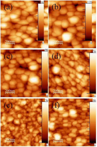
Figure 7 AFM images for (a) undoped, (b) 1, (c) 4.8, (d) 6.5, (e) 23.8 and (f) 33.3 at% Zn/Sn films. The Z direction (perpendicular to substrate) scale are in nm for all images.
Table 2 Roughness and mechanical properties H and E according to the texture direction.
Sample |
[Zn]/[Sn] in Solution (at.%) |
RMS roughness (nm) |
Hardness (H) (GPa) |
Elastic Modulus (E) (GPa) |
Texture Weight (wt%) |
|
(200) |
(101) |
|||||
Substrate |
11 ± 1 |
92 ± 1 |
||||
ZN01 |
0.0 |
17 ± 1.7 |
12 ± 1 |
138 ± 10 |
||
ZN02 |
1.0 |
21 ± 0.5 |
22 ± 1 |
168 ± 5 |
93 |
7 |
ZN03 |
2.9 |
18 ± 1.7 |
21 ± 1 |
195 ± 4 |
55 |
45 |
ZN04 |
4.8 |
15 ± 1.8 |
23 ± 1 |
195 ± 7 |
51 |
49 |
ZN05 |
6.5 |
11 ± 0.2 |
23 ± 2 |
176 ± 6 |
59 |
41 |
ZN06 |
9.1 |
20 ± 1 |
158 ± 5 |
44 |
56 |
|
ZN07 |
23.8 |
9 ± 1.1 |
19 ± 2 |
140 ± 6 |
3 |
97 |
ZN08 |
33.3 |
8 ± 0.3 |
20 ± 3 |
147 ± 4 |
8 |
92 |
The domain shapes and crystallinity were studied by TEM techniques, Figure 8 shows the micrographs and their corresponding Selected Area Electron Diffraction (SAED) patterns are include. Figure 8a shows bright field TEM image for undoped SnO2 film, without texture and its domain morphology exhibit different particle shapes, such as: globular (R), elongated (E), twinned (T) and quadrilateral (Q), each type were labeled in the micrograph. Figure 8b shows dark field and bright field (inset) TEM micrographs for film with 1 at% of Zn/Sn, this film is textured in the (200) direction; in this case most of crystallites have globular shape. Figures 8c and 8d show bright field and dark field micrographs TEM for sample with 4.8 at% Zn/Sn, respectively. In this case most of the domain crystallites are elongated, this sample has texture in the (200) and (101) direction, these elongated particles growth in the (101) direction such as it can be seen in the atomic resolution image (Figure 9c)

Figure 8 TEM micrographs at bright and dark field for (a) undoped, (b) 1 dark field, (c) 4.8 bright field, (d) 4.8 dark field, (e) 23.8 and (f) 33.3 at% Zn/Sn. inset images at higher magnification and SAED patterns
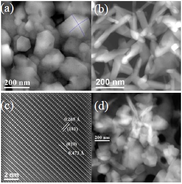
Figure 8e shows bright field TEM micrograph of the film with 23.8 at% Zn/Sn, in this image can be noticed the presence of two different types of domain particles: globular and short-extended, the texture of this sample is almost (101). Finally, Figure 8f displays bright field TEM micrograph of sample with 33.3 at% Zn/Sn, it can be appreciated that most of the domain particles have globular or quadrilateral shape, the texture of this sample is (101) direction completely. There is no direct correlation between the shape of particles and texture growth direction of the samples according to TEM and XRD results. It is interesting to observe changes in the films’ microstructure, all of them showed well-defined domain particle, each one had a dominant shape of particles and these changes are due to the Zn dopant quantity content. The selected area electron diffraction (SAED) are include inset of these images, all of them index well with SnO2.
The shape of the domains could be visualized better by STEM technique. Figure 9 shows STEM images acquired with HAADF detector (Z contrast), these images show apparently 3D shape of the particles. The micrograph in the Figure 9a is for undoped sample, it shows clearly the quadrilateral shape particles, which are squared base pyramids, this particle morphology has been visualized due to the HAADF detector, and it generates clear thickness contrast. The images in Figures 9b and Figures 9c are for 4.8 at% Zn/Sn sample, it can be remarked that these elongated particles are not flat, they have thickness with different wide values and the end of them have a tip without well-defined shape. This changes in morphology let us understand the influence of Zn as dopant in the material. The micrograph 9c shows the atomic resolution image with Z contrast in a STEM mode, this image present 0.473 nm and 0.265 nm d-spaces values which belongs to (010) and (101) directions, respectively. The last image (Figure 9d), shows the domain particles for 23.8 at% Zn/Sn sample, it shows two types of particles, globular and elongated, these particles do not show a clear shape.
Thin film d-spaces parallel to the substrate was visualized by images acquired with STEM technique. Figure 10 shows the cross section images for samples with 1 and 23.8 at% Zn/Sn, which are textured along (200) and (101) direction, respectively. The samples were made by FIB, for this reason it was previously covered with Au layer (protection for sample preparation). Micrographs in Figures. 10a and 10b are for 1 at% Zn/Sn doped sample, which has texture in the (200) direction. The image in Figure 10b shows 2.39 Å SAED pattern inset show two spots with the highest intensity that belong to (200) direction; there are other diffraction patterns spots, but they have less strong intensity. The images in Figures. 10c and Figure 10d are for 23.8 at % Zn/Sn doped sample, this film has (101) direction texture, the lattice distance shows (101) d-spaces parallel to the substrate; The SAED pattern is inset in the same image, it shows symmetric strong pattern intensity in the (101) direction. These thin films cross section images confirm the textured direction due to the Zn dopant quantity content.
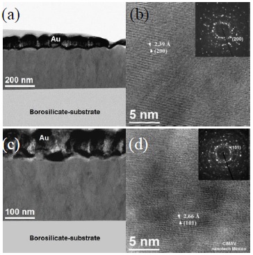
Figure 10 STEM cross-sectional view images for textured samples: (a) low mag and (b) HREM image for 1 at% Zn/Sn; (c) low mag and (d) HREM for 23.8 at% Zn/Sn; inset are the SAED patterns.
According to the domain particles’ shapes of the Zn doped SnO2 thin films, the detected texture by XRD patterns is related with a specific morphology, which were revealed by electron microscope images acquired at different modes. According to this characteristics, we studied the influence in their MPS and results are shown at the next item.
Nano-mechanical properties
The hardness (H) and elastic module (E) were determined for each studied sample in nine positions, including for the glass substrate without thin film as reference. Figure 11a shows AFM image with nine residuals indentation positions matrix. The typical results were shown in Figure 11b, it is the characteristic behavior between force and displacement penetration depth. The basic nanoindentation analysis from the load-displacement curve (F-h) was established based on the elastic contact theory given by Sneddon [32] and Doerner et al [33] considering the glass substrate (corning 7059 without thin film) as a bulk. The H and E measurement values for the substrate was 11 ( 0.5 GPa and 92 (0.5 GPa, respectively.
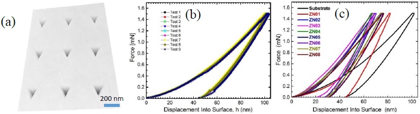
Figure 11 AFM image of (a) residual matrix indent and (b) characteristics depth vs force curves from nanoindentation tests for substrate (Corning 7059). Variation of depth vs force curves for (c) all samples.
On the other hand, the H and E values for Zn doped SnO2 thin film were measured by Continuous Stiffness Measurement (CSM) methodology [34]. This is accomplished by superimposing a small oscillation on the primary loading signal and then analyzing the response of the system by means of a frequency-specific amplifier; this was done to measure the MPs of the films without the influence of the substrate. The equation to determine the stiffness (S) in CSM test is the following:
In this experiment the excitation frequency (ω) value is set. Thus S was evaluated by measuring the displacement amplitude (Z0), phase angle (φ) and the excitation amplitude (F0). Other parameters such as load-frame stiffness Kf, the stiffness of the support springs Ks and mass m are known previously for a specific measurement instrument. With a CSM method the H and E are measured as a function of penetration (h). The measurement for each sample was taken from 9 different zones (Figure 11a) to determine the average value, it was made to detect some mechanical properties’ changes. The H and E values previously measured for the alone substrate and the values for undoped SnO2 sample were used as a reference to determine the influence of Zn quantity content in the MPs of Zn doped SnO2 films.
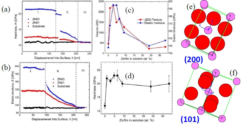
Figure 11c shows the characteristic load-penetration curves for each study samples. In this figure, we can see the variation of depth penetration. The mechanical behavior is elastic-plastic for all samples due to the shape of graphics [35]. The hardness and elastic modulus as a function of the penetration depth is presented in figure 12a and 12b, respectively. Figure 12a shows the hardness behavior for three representative samples as a function of penetration depth (substrate, ZN01 and ZN03). In these figures, we can distinguish three interval: region I which correspond to the thin film hardness only (0 - 125 nm penetration depth), in this region there is no influence from substrate; being this methodology well-established criterion in the literature [36]. Thus, the hardness of the samples ZN01 and ZN03 correspond to 12 and 21 GPa, respectively. In the case of substrate (reference) it remains constant at H = 11 GPa. In the region II the hardness of the thin film is influenced by the substrate, it is due to both values start decrease. Finally, in Region III the hardness is completely influenced by the substrate, that is to say depth penetration reached to the substrate.
On the elastic modulus, Figure 12b shows its behavior as a function of penetration depth for both samples and substrate, it has analogous behavior to the hardness. These elastic modulus for films ZN01 and ZN03 correspond to 137 and 195 GPa, respectively. Table 2 shows the H and E values behavior as a function of Zn dopant content. In general, the presence of Zn atoms in SnO2 thin film enhanced their MPs, these values are higher than undoped sample. The highest hardness and elastic modulus are obtained when the dopant level is around 4.8 at% of Zn/Sn, with hardness 23 ± 1 GPa (see Table 2), this value is 95 % higher than undoped sample; related to the elastic modulus it reaches 195 ± 7 GPa, it being 42 % higher than undoped sample. However, for Zn dopant quantity with higher content than 4.8 at%, it is detrimental to the mechanical property; but the values are still higher than pure SnO2 sample. Using similar methodology, the MPs values for F doped SnO2 films obtained by chemical vapor deposition show 5.1 and 71.1 GPa for hardness and elastic modulus, respectively [37]. In our case, H and E values for Zn doped sample are higher than F doped SnO2. According to these values, our measurements are in the range.
The main influence in the MPs is due to the textured direction of the grown thin film, as a consequence of Zn dopant quantity content in the SnO2. Figure 12c shows the behavior of elastic modules and (200) texture direction (IPF values) as a function of Zn dopant content in SnO2 thin film; these IPF values show high correlation with the elastic modulus measurements, it means the E value is related with the crystal orientation. Figure 12d shows the hardness values versus the amount of the Zn dopant in the SnO2 thin films; it can be noticed that for all dopant contents, samples show higher H value than undoped sample. From these performance, it can be noticed clearly that around 5 % at. Zn/Sn content sample present highest H and E values. This behavior is due to the textured direction of the thin film; it means the orientation of the unit cell on the substrate film is important to improve mechanical properties of SnO2 as thin film. Figures. 12e and 12f show the atoms arrangement according to the unit cell orientation along (200) and (101) texture direction, respectively. The atoms organization when the growth is along (200) direction are more compact than for (101) direction grown; it means, according to these atoms arrangement, the material change its MPs. Therefore, it could be concluded the ZN03 and ZN04 samples show better texturization (parallel to the substrate). Among the studies samples set in this report, they have better MPs due to the presence of both (200) and (101) crystal orientation direction with the same proportion (see Table 2 texture weight percentage column).
Conclusions
Textured films were synthesized by the spray pyrolysis technique, using an alcoholic solution of SnCl4.5H2O and zinc acetate. It was demonstrated that this synthesis technique provides a powerful tool for creating a specific film structure orientation; it was shown that the influence of dopant concentration in start dilution affects the texture and shape of domain particles. A semi quantitative evaluation of inverse pole figure in the normal direction to the surfaces was obtained; d-spaces in the direction (200) and (101) have a marked tendency to grow parallel to the substrate; according to the Zn dopants content. The measured Young´s module and Hardness values are higher than undoped materials; being this synthesis method adequate to change MPs of the SnO2 film. The measured Young´s module show high correlation with the (200) growth texture direction. The MPs in this material is anisotropic, it changes according to the unit cell orientation on the substrate. These thin films with mechanical properties improved are ready to many technological applications.

