


 nueva página del texto (beta)
 Inglés (pdf)
 Artículo en XML
 Referencias del artículo
 Enviar artículo por email
 Citado por SciELO
  Similares en
SciELO
Similares en
SciELO 
 Permalink
Introduction
Spintronics is a branch of electronics that in addition to the use of the electron's charge, it also uses the electron's spin known as an additionally degree of freedom. The use of both the spin and the charge of the electron allows the fabrication of new functional devices with improved characteristics compared to those where only the electron's charge is used [1], such as spin valves, magnetic tunnel junctions and spinfield effect transistors (spin-FET) [2]. The design of these devices is based on the magnetic characteristics of the materials employed for their fabrication. One of the major challenges on the design of spintronic devices, as the spin-FET, is the achievement of spin injection into a semiconductor at room temperature (RT) [3]. The efficiency depends on the quality of interfaces. For this purpose diluted magnetic semiconductors (DMS) seems to be a good solution as there are no crystallograpic interfaces between a semiconductor and a DMS based on the same matrix of the substrate [4]. However, the low Curie temperature (TC) and also the formation of precipitates is a limitation for their use at RT [5-7]. On the other hand, the use of tunneling oxide barriers such as Al2O3 or MgO has provided a solution for the growth of ferromagnetic layers on IV-group semiconductors. In this case, the limitation is due to the several interfaces that the electrons have to overcome from the ferromagnetic (FM) injector to the semiconductor through a tunneling barrier, leading to a loss of the spin coherence [8]. Spin injection by tunneling into a semiconductor, via a schottky barrier, can be achieved by a FM material directly grown on a IV-group semiconductor [9]. A material that has been proposed for an efficient spin injection is the Ge(001)/Mn5Ge3 heterostructure [10,11].
Mn5Ge3 is a FM compound with a magnetization of 1200 kAm-1 a polarization of 42% and a TC = 296 K [12,13]. Mn5Ge3 has a hexagonal crystal structure P63/mcm, and lattice parameters a = 7.184 Å and c = 5.053 Å, which allows the epitaxial growth on Ge(111) substrates within a lattice mismatch of 3.7% [14-16]. The crystal structure is formed by two Mn sublattices, Mnl with atomic positions at (0.236, 0, 1/4), MnlI with atomic positions at (1/3, 2/3, 0) and Ge at (0.5991, 0, 1/4).
Mn5Ge3 is the unique FM phase in the Mn-Ge phase diagram [17]. The theoretical magnetic moment per Mn atom is m = 2.99 μΒ that is in agreement with the experimental value m = 2.6 µΒ [18]. The origin of ferromagnetism in the compound is mainly due to the MnII sublattice. A way to increase the TC is through carbon doping, where the C atoms are placed interstitially in the center of the octahedron formed by the MnII atoms. The role of carbon atoms is to modify the electronic structure of Mn5Ge3 and secondarily an enhancement of the super-exchange interactions [14,19,20].
To successfully integrate Mn5Ge3 into the Si technology it is necessary to grow the compound on Ge(001) substrates, which are compatible with Si(001) [21]. The integration can be achieved within the following stack Si(001)/GeSi(001)/Ge(001), thus Ge(001)/Mn5Ge3 is an important candidate to be used as an spin injector into IV-group semiconductors, which are widely used in most of the microelectronic devices [22].
In this paper we report on the growth of Mn5Ge3 on Ge(001) substrates in a range of temperatures between 650 and 850 °C. Above 750 °C a small amount of Mn5Ge2 is formed. Regarding the C-doping the TC was increased form 296 to 390 K in a concentration of Mn5Ge3C0.06. The low magnetization is a desirable characteristic to allow faster spin-transfer torque (STT) process on spin-FETs.
Experimental methodology
Substrates preparation
Prior to the introduction of the samples to the growth chamber an ex-situ wet chemical cleaning is carried out with trichlorethylene, acetone and ethanol in sequential ultrasonic baths. The samples are rinsed with deionized water and dried with air. Then an in-situ thermal cleaning inside the growth chamber consists in degassing the sample at 450 °C for 3 h, followed by a biased plasma etching on the substrate at 40 W for 20 min, to remove the native germanium oxide from the surface. Finally, a high temperature annealing at ~750 ° C for a few minutes is performed until a 2×1 substrate reconstruction is observed by means of reflection high-energy electron diffraction (RHEED), which indicates that the substrate surface is atomically clean and flat, which is a necessary condition for epitaxial growth.
Deposition technique and methods
Magnetron-sputtering technique is used for the growth of Ge(001)/Mn5Ge3 thin films with a nominal thickness of 50 nm. The Mn5Ge3 thin films were grown by codeposition of Mn and Ge at different temperatures using radio-frequency power sources operating at 45 and 30 W, respectively. The Mn5Ge3 rate deposition is 2.9 nm/min. The codeposition of Mn and Ge at different substrate temperatures (Ts) is known as the reactive deposition epitaxy (RDE) method as the solid reaction between add-atoms takes place at the moment they reach the substrate surface.
Results and discussion
X-ray diffraction
The X-ray diffraction (XRD) patterns, performed in grazing incidence of the samples synthesized at 650, 750 and 850 °C and the C-doped sample grown at 750 °C are shown in Figure 1. The XRD patterns reveal mainly the existence of the Mn5Ge3 phase. At temperatures between 650 and 750 °C one can observe the existence of small Mn11Ge8 clusters, however as shown later in the magnetic M-T measurements, there is no measurable signal attributed to this phase. Additionally, the hexagonal Mn5Ge2 phase, which is also antiferromagnetic, is observed for the growth at 850 °C and for the C-doped sample at 750 °C. Matsui et al., also reported that T s higher than 700 °C favors the growth of the Mn5Ge3 phase while the Mn11Ge8 phase disappears [23] (as shown in the inset in Figure 1). It can be established that in the sample grown at 850 °C and the C-doped sample grown at 750 °C, a majority Mn5Ge3 phase is obtained in form of thin films on Ge(001) with a small amount of Mn5Ge2 nanoclusters. Regarding the Mn-Ge phase diagram the Mn11Ge8 phase, which is antiferromagnetic, is formed between 350 and 750 °C. It can also be noted that at higher temperatures (i.e. 796 °C) Mn5Ge3 dominates the phase formation.

Atomic force microscopy
The atomic force microscopy (AFM) images shown in Figures 2(a) to 2(c) reveal the surface topography of the samples synthesized at 650, 750, 850 °C and the topography of the C-doped sample grown at 750 °C is shown in Figures 2(e) and 2(f). The root mean square (RMS) roughness of the samples increases with increasing Ts, RMS = 32, 51 and 96 nm for the growth at 650, 750, 850 °C, respectively. The C-doped sample grown at 750 °C compared to the undoped sample grown at the same temperature shows a RMS roughness of 24 nm, this roughness reduction (i.e. from 51 to 24 nm) is accompanied with a grain size reduction from ~450 nm for the undoped sample to ~100 for the C-doped sample. The line profile of the AFM micrograph of the C-doped samples Figure 2(g) shows a close-packed arrangement of the grains implying a continuous coverage growth obeying to a Volmer-Weber growth mode. On the other hand, the undoped samples obey also to a Volmer -Weber growth mode but as seen on the line profile scan in Figure 2(d) it is clear that Mn5Ge3 do not cover homogeneously the Ge substrate, only 3-dimensional islands are observed [Figures 2(a)-2(c) ]. Two diagrams describing the Volmer-Weber growth modes of the undoped and doped samples are shown in Figures 2(h) and 2(i), respectively. Finally, the scanning electron micrograph of a cross section of the C-doped sample confirms the suggestion of the growth mode [Figure 2(j) ]. The surface free energy of the Ge(001) substrate is 1710 erg/cm-2, the fact that C-doped Mn5Ge3 forms a close-packed grain arrangement on the Ge surface implies a higher surface free energy than that of the undoped compound, but still lower than that of the substrate. According to the Young's equation, a continuous film is obtained if y s ≥ у int + yf where γ represents the surface energy of the f (film), s (substrate) and int (interface). If y s < y int + yf, the growth corresponds to a 3-dimensional island-like growth leading to bare substrate regions surrounding the islands as in the case illustrated in Figures 2(a)-2(c). Thinner films may exhibit a lower surface roughness allowing nanolithography patterning for the fabrication of for example the source and drain of a spin-FET transistor.
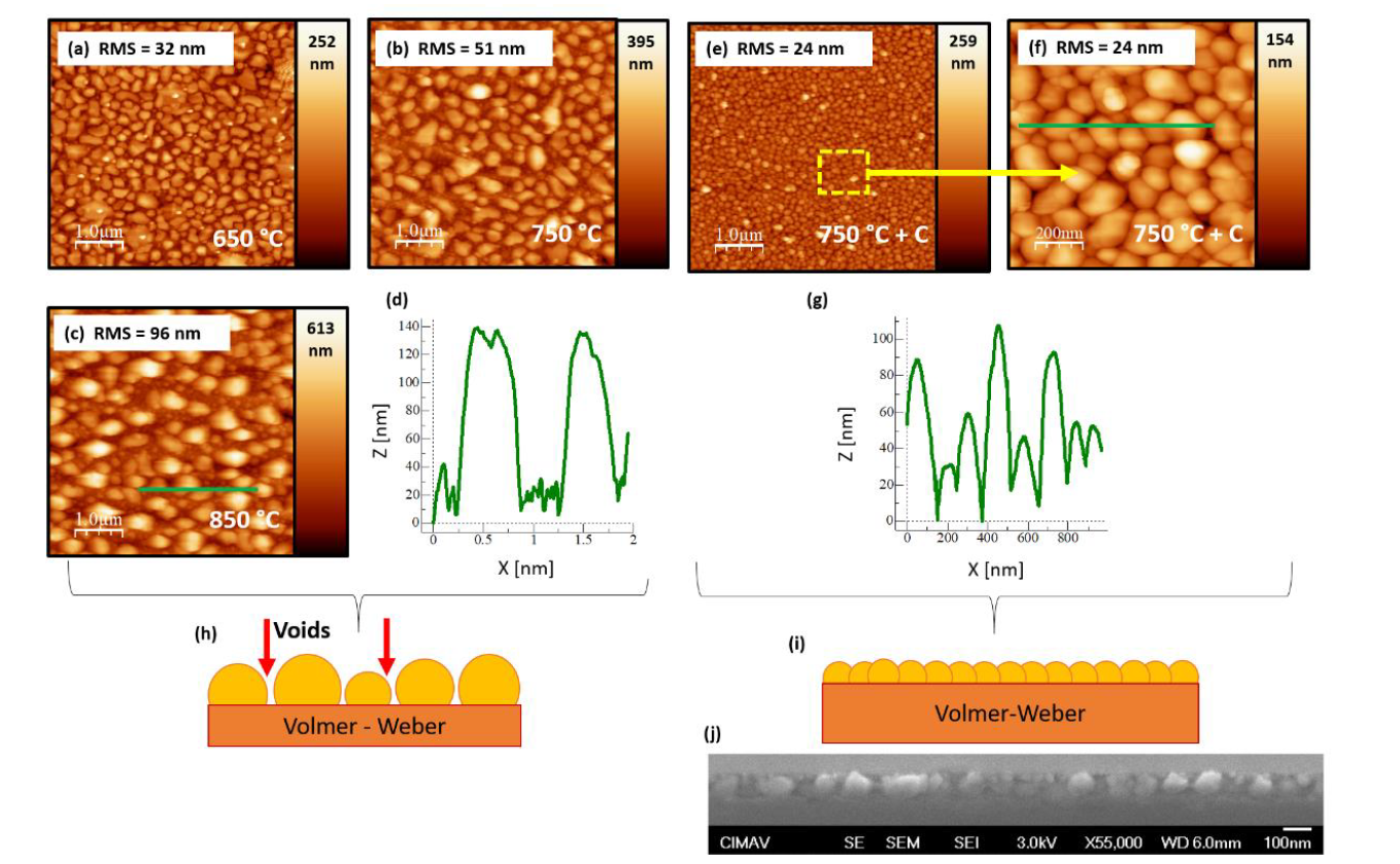
Figure 2 Atomic force microscopy images of the films grown at (a) 650 °C, (b) 750 °C, (c) 850 °C and (d) the C-doped sample grown at 750 °C. (e) The Volmer-Weber growth mode representation for the undoped samples and (f) the Stranki-Krastanov growth mode for the C-doped sample.
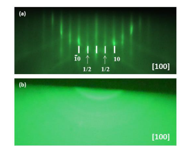
Figure 3(a) shows a RHEED pattern of a 2x1 reconstructed Ge(001) surface along the [100] direction indicating that the surface is atomically smooth prior to thin film growth. Figure 3(b) reveals the RHEED pattern taken inmediately after the initial stage of the deposition, the diffusive nature of the pattern indicates that the surface is rough due to the 3-dimensional island growth, confirming the information obtained from the AFM experiments, concluding that the growth obeys a Volmer-Weber growth mode.
Magnetic properties
Figure 4 shows the M-T plots, under an applied magnetic field of 2 T, ensuring saturation of the films, for all samples. It can be observed that the C-doped sample has the highest Tc = 390 K compared to ~300 K for the undoped samples. The Tc was determined by the fit of the experimental data with the equation:
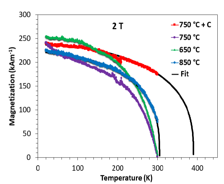
Figure 4 M-T of all samples. The T C was obtained from the fit of the experimental data using Eq. 1. The C-doped sample has a T C of 390 K.
where m = M s /M o and τ = T/Tc are the reduced spontaneous magnetization and reduced temperature, respectively, and s and p are parameters with p > 3/2 and s > 0 [24]. Furthermore, the saturation magnetization obtained in this sample Ms = 250 kAm-1 is much lower than that of samples grown at 250 °C, grown by magnetron sputtering reported earlier (Ms = 633 kAm1, Ref. 13) and lower than 1200 kAm-1 for Mn5Ge3 thin films grown on Ge(111). The reduction of Ms may be due to the formation of dead magnetic phases, usually appearing at the interface with the substrate but also at the surface of the film (when high roughness) and at the intergrain boundaries. This achievement is considered a great advantage over the samples grown at lower T s . STT is a mechanism where a spin-polarized electric pulse switches the magnetic orientation of a FM layer, a requirement to reduce the magnitude of the electric pulse and the required time to achieve the switch is a low Ms of the FM material. Additionally the material has been grown on Ge(001) substrates which are compatible with the Si(001)-complementary metal-oxide-semiconductor (CMOS) technology. This feature combined with the enhancement of the T c up to 390 K, makes Ge(001)/Mn5Ge3C0.6 grown at 750 °C a perfect candidate for spintronic applications. Hence, materials with low magnetizations are required for the fabrication of magnetic tunnel junctions with low energy consumption. The shape of the curves in the M-T graph corresponds to ferromagnetic materials, as no additional peaks characteristic of the antiferromagnetic-FM transition of Mn11Ge8 are observed along the decreasing curve.
Conclusions
Mn5Ge3 epitaxially thin films were grown on Ge(001) substrates by reaction deposition epitaxy method. Undoped Mn5Ge3 thin films grew in a 3-dimensional mode while the effect of C-doping at a concentration of Mn5Ge3C0.6 allows a closed-packed grain arrangement leading to a low roughness and a homogeneous grain size; the growth mechanism corresponds to a Volmer-Weber growth mode. At high temperatures the Mn5Ge3 phase appears accompanied with small nanoclusters of Mn5Ge2, which are antiferromagnetic. The carbon doped sample showed an increase from 296 K, for undoped samples, to 390 K. The value of the saturation magnetization is ~250 kAm-1, which represents an advantage in the development of low power consumption spintronic devices using the spin-transfer torque process that requires of low current pulses and hence a rapid switching based on low magnetization devices.

