


 nueva página del texto (beta)
 Inglés (pdf)
 Artículo en XML
 Referencias del artículo
 Enviar artículo por email
 Citado por SciELO
  Similares en
SciELO
Similares en
SciELO 
 Permalink
Introduction
Self-Assembled Quantum Dots (SAQDs) have been intensively investigated due to the interest from a fundamental physics point of view [1-3] and for their potential in technological applications [4-7], such as lasers [7-9], photodetectors [10-12], light emitting diodes [13,14], THz emission devices [15] and solar cells [16-18]. One of the systems most studied consists in InAs/GaAs quantum dots grown by Molecular Beam Epitaxy MBE [19].
The optical properties of InAs/GaAs QDs have been investigated via photoluminescence (PL) and photoluminescence excited (PLE) techniques [20-22], but the information obtained is often limited to only the lower energy states, which does not allow a deduction of the shape of QD potential. However, other methods, such as electroreflectance (ER) [23-25], reflectance-difference [26] and photoreflectance (PR) [16,23-24,27-28] techniques can detect higher energy transitions in the QD and other layers.
Investigations have focused on optical transitions around the quantum dots [29] and the wetting layer, while few works have been done considering the effect of photoexcited free carriers in buffer layer traveling to the surface, i. e., towards QDs [28,30].
The signals under consideration in the measured PR spectra were GaAs band gap transition and higher-energy transitions associated to Franz-Keldysh Oscillations (FKOs). It is known that PR spectra can be classified depending on the electric field strength in depletion region [24,28], and thus, the appearance of FKOs in the PR spectrum indicates medium field regimen. These spectra were fitted by using a damped FKO above the gap originating from the epitaxial GaAs surface. From analysis we obtained the electric field, broadening parameter and electro-optical energy for InAs/GaAs QDs sample and a GaAs commercial sample. FKOs periods are related also to the effective mass µ [25]. Alperovich et al. [31] and Wang et al. [32] proposed that sharp Higher Holes (HH) and Light Holes (LH) transition peaks can be observed after taking the fast fourier transform (FFT) to the FKOs line shapes [25]. The ratio of the square root of the HH and LH reduced mas, µLµH)1/2, was obtained from the relationship of the main frequencies [33]. Also the band bending energies were studied in both, InAs/GaAs and GaAs samples. The electric field, broadening parameter, electro-optical energy, the reduced mass effective and the band bending energy are important parameters when developing optoelectronic devices due to they could affect the photoresponse. Similarly, in the development of optoelectronic and electronic devices, an important feature that allows evaluating performance is the response time. One of the mechanisms that influence the response time of a device is the interaction between the density of surface traps and free carriers, known as the trap-filling time (τ) [34,35], as recently reported by our group [11], in the same systems (GaAs and InAs/GaAs QDs), finding that the presence of QDs increases the value of τ.
Therefore, in this work we present PR spectra measured at room temperature in an InAs QDs layer grown over a 200 nm GaAs buffer layer in a GaAs substrate and a GaAs commercial sample. We also discussed the buffer layer effect as host for InAs QDs.
Experimental and theoretical details
InAs self-assembled quantum dots (SAQDs) were grown by Molecular Beam Epitaxy (MBE) through the Stranski-Krastanow process. QDs are formed by depositing a few InAs monolayers on an InAs wetting layer with 2D growth, which copies the network of the GaAs (1 0 0) substrate, and then, it is stressed up to a critical thickness (~1.7 monolayers -ML-) to form three-dimensional quantum structures (sample Q.dots90) [36], as shown in the AFM image in Figure 1a). In Figure 1b) it is observed the histogram with the number of dots in a selected area (red in Figure 1a) in relation with their height in Å. GaAs is an undoped sample from a commercial wafer with an orientation (1 0 0) ± 0.1°, acquired from Wafer Technology.

Figure 1 a) AFM image of quantum dots. b) Histogram with the number of dots in relation with its height.
Photoreflectance technique experimental set-up for optical characterization is presented in Figure 2. It consists of an optical set-up for focusing and positioning the probe and the modulated beams, a device for measuring the reflected probe beam intensity, and several electronic devices for detecting the signal and driving the experiment. The sample is located onto a holder. The two light beams illuminate the sample in the same place. A monochromator, by using a 250 W tungsten lamp as a probe source, is controlled by a PC and generates the first beam (probe beam), which is continuous and arrives focused onto the sample surface. Its wavelength runs within a range depending on what will be measured, in our case, from 820 nm to 960 nm. The modulated beam is a continuous Ar+ laser whose maximum power is 21 mW. Its intensity is modulated by a mechanical chopper operated at frequencies up to 3000 Hz. This is the beam responsible for modulating the sample surface electric field.

The probe beam reflected by the sample surface is detected by a photodiode. An optical filter prevents any influence of light scattered from laser in the detector. The output signal of the detector is sensed by a lock-in amplifier, phase and frequency sensitive, in order to separate from background signal, the response of the sample that has a frequency matching the modulation frequency [11,37,38]. This is achieved tuning the lock-in amplifier to the frequency and phase of the chopper. The information delivered by the amplifier corresponds to the change of reflectivity AR. The output signal of the detector is also sensed by and a milivoltmeter which takes the constant value of the signal corresponding to the Reflectivity R. ΔR/R is the value plotted over the photon energy. All measurements were carried out at room temperature.
Theory
The mechanism of PR technique is the modulation of the surface electric field by generating electron-hole pairs, which modify the distribution of surface electric charge changing the curvature of the energy bands [39].
Photoreflectance spectroscopy is a powerful tool, contactless and nondestructive method for characterization of optical transitions in semiconductors; it gives useful information about electronic structure of investigated materials. In particular, it is possible to determine the energy and broadening parameter of the observed features that appear at energies corresponding to the band gap critical point. Even weak features, which are not clearly visible in usual, stationary reflection spectra, can be strongly enhanced in PR even at room temperature [40], so they can be determined with accurately for transitions from a detailed lineshape fit to the experimental data. In most PR experiments, where the low-field limit is performed, the critical-point energy is determined by fitting the shape of the signal at the band edge with the third-derivative (TDFF) Aspnes model [41,42]:
where Eg is energy band gap, C is broadening parameter, θ is the phase factor and Γ is the broadening parameter. Parameter n depends on the critical point type and the derivative order [38].
For higher values of the electric field, oscillations appear in the spectrum at higher energy values than the critical point. These oscillations are known as Franz-Keldysh Oscillations and when becoming prominent indicate the field is in the intermediate field regimen. Aspnes found that this is possible if |ħΩ | ≥ Γ [43], ħΩ is the electro-optical energy.
For the analysis of the experimental data on the middle-field regime, Aspnes and Studna [42] propose that the PR spectrum can be described by:
where Φ is a phase factor which depends on the strength of electron-hole interaction, processes of short-range dispersion and the critical point dimensionality, ħΩ represents the energy gained by photoexcited carriers due to the applied electric field modifies the bending of the bands on the material surface. It is related to the electric field F by:
where e represents the electron charge, µ is the reduced interband effective mass in the direction of F, ħ is the Planck constant and Eg is the band gap energy [43].
Whereas the laser light beam is responsible for the modulation of the bands in the semiconductor material, ΔR/R depends upon the beam intensity and considering photovoltaic effects, this dependence can be expressed [44]:
where K is the Boltzmann constant, γ is the quantum efficiency of the material, hv is the modulator beam energy, T is temperature in K, R is the reflectivity on the surface on which the beam strikes, Pm is the modulator beam power, eVs is the band bending energy, e is the electron charge and C = (A*T2)/e, A is the Richardson effective constant.
Results and discussion
Figure 3a) shows PR spectra in InAs/GaAs quantum dots at 300K fitted by using expression (2). Energy gap associated to GaAs is observed in 1.42 eV, and the Franz-Keldysh Oscillations (inset) appear in the spectrum at higher energy values than the critical point, as expected. In Figure 3b) is presented the FFT from InAs/GaAs PR spectrum, and it is observed the value for the frequency of light and heavy holes in 38.7 eV-3/2 and 58.9 eV-3/2, respectively.

Figure 3 a) InAs/GaAs PR spectrum fitted by using expression (2). b) FFT from InAs/GaAs PR spectrum.
PR spectra fitted with expression (1) in commercial GaAs is shown in Figure 4a). The value of the energy bandgap is observed in 1.42 eV, and highly damped Franz-Keldysh Oscillations are observed. Figure 4b) shows the FFT GaAs PR spectrum and we determined the frequency of light and heavy holes values of 23.9 eV-3/2 and 32.7 eV-3/2, respectively. Table 1 presents the values calculated.

Table 1 Electric field, broadening parameter, electro-optical energy and the reduced mass of the HH and LH values in the studied samples.
| Sample | P | fchop | F | Г | ħΩ | fLH | fHH | (µL/µH)1/ 2 |
| (mW) | (Hz) | (kV/cm | (meV) | (meV) | eV3/2) | (eV3/2) | ||
| InAs/Gas | 7.87 | 3.26 | 7.21 | 38.69 | 58.9 | 0.66 | ||
| 20 | 255 | |||||||
| GaAs | 11.12 | 9.70 | 9.10 | 23.9 | 32.7 | 0.73 |
Table 1 also presents electric field values on the surface for both samples, and it is observed a weak reduction in the value obtained for InAs/GaAs quantum dots of one order of magnitude compared to the one obtained for GaAs. The presence of these nanostructures could generate effects of localized carriers' confinement in the buffer layer and homogenize the surface electric field, inducing surface passivation.
Figures 5a) and 5c) show the PR spectra in InAs/GaAs quantum dots and GaAs samples for different powers of the modulator beam at 255 Hz. From analysis of these spectra we obtained the PR intensities. The modulator beam power dependence with the PR intensities is presented in Figures 5b) and 5d). These results were fitted by using expression (4) and we determined the band bending energy eVs values as presented in Table 2, and agree with recent report [45]. We found when increasing the modulator beam power, PR intensities increase due to variation of band bending energy at temperature fixed. The difference between Figures 5b) and 5d) can be attributed to a slight increase in the band bending energy value in InAs/GaAs, as shown in Table 2, possibly associated to local changes in the bands energy offset.
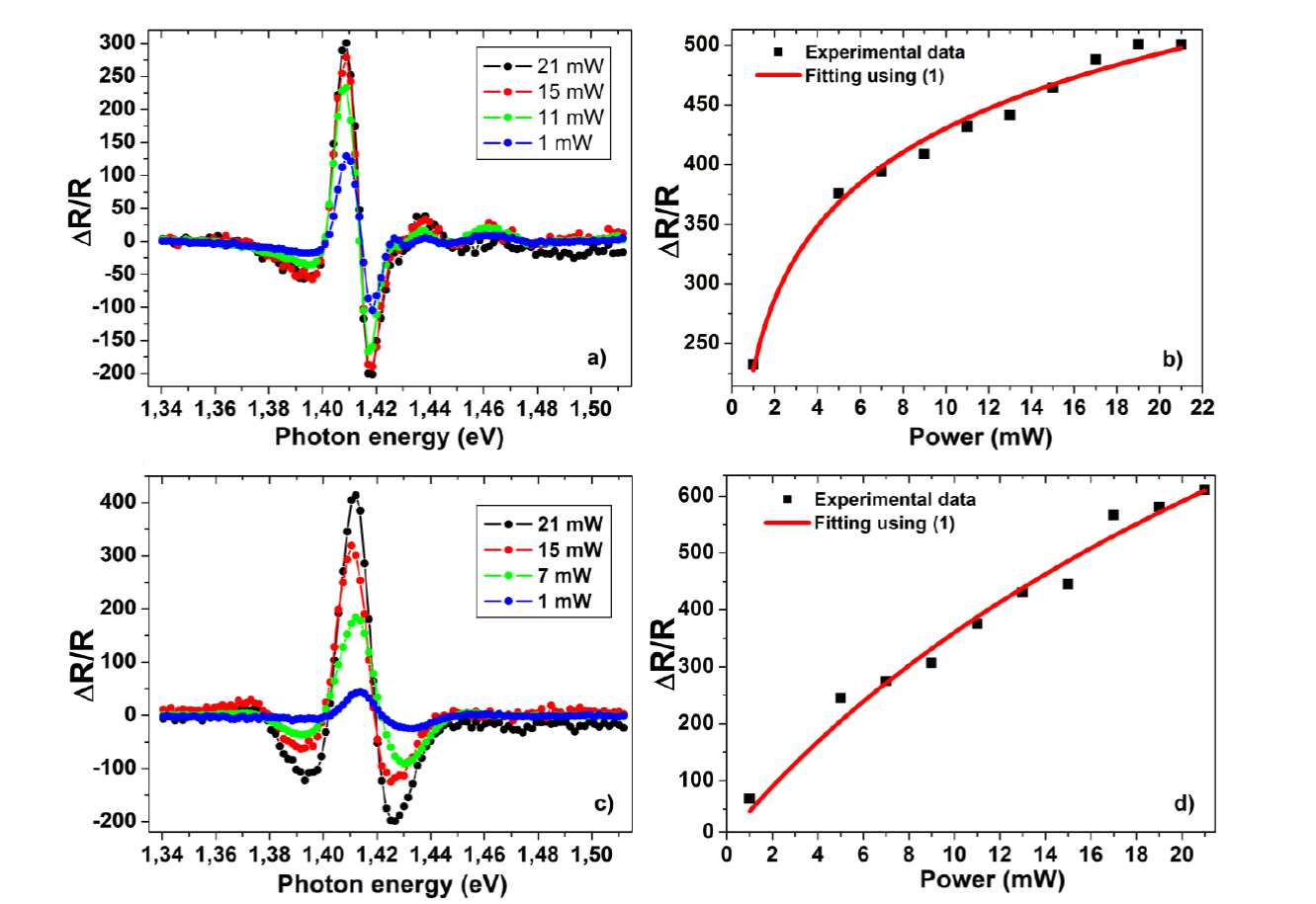
Figure 5 a) InAs/GaAs PR spectra for several modulator beam intensities at 255Hz. b) PR intensities as a function of the modulator beam power in InAs/GaAs PR spectrum. c) GaAs PR spectra for several modulator beam intensities at 255Hz. d) Modulator beam power dependence with the PR intensities in GaAs PR spectrum.
Conclusions
InAs/GaAs QDs sample PR spectra were obtained and compared with a commercial GaAs sample PR spectrum, and they were analyzed by using the derivative Lorentzian functions as proposed by Aspnes in the middle field regimen. The parameters analyzed were the electric field on the surface, the broadening parameter, the energy gained by photoexcited carriers due to the electric field applied, the frequency of light and heavy holes and the bending energy values. The results suggest that the presence of InAs quantum dots increases the light and heavy holes' frequencies and the bending energy values and decreases the electric field on the surface, the broadening parameter and the energy gained by photoexcited carriers. We found that InAs QDs presence modifies the surface electrical field around one order of magnitude in the GaAs buffer layer and this behavior can be attributed to surface passivation.

