


 nova página do texto(beta)
 Inglês (pdf)
 Artigo em XML
 Referências do artigo
 Enviar este artigo por email
 Citado por SciELO
  Similares em
SciELO
Similares em
SciELO 
 Permalink
Introduction
The MEMS (Micro-Electro-Mechanical Systems) acronym is commonly used to describe mechanical structures of micrometric dimensions performing an electronically controlled preset function [1]. Currently, the MEMS (mechanical-microstructures) offered by manufacturers usually consist of sensors and/or actuators that are separately fabricated and then bring to interaction with electronic circuitry (hybrid integration); such hybrid systems show many functional drawbacks mainly due to external wiring [2]. Nevertheless, MEMS is an evolving technology and includes more than just mechanical structures, also includes a wide number and variety of microcomponents (chemical, thermal, magnetic, mechanical, etc.) and electronic circuits. According to the nature of the microcomponents, the full potential of MEMS products has been possible only by its proper integration with a specific conditioning electronic circuit. In this sense, nowadays MEMS designers are facing different possibilities for integrating a monolithic system (combining sensors/actuators and electronic devices on a single substrate) based on the careful selection of both modules: micro-structures/components and CMOS circuits [2]. MEMS designers can choose from Pre-CMOS, Post-CMOS and Intra-CMOS approaches. Each one of these approaches includes a set of fabrication steps to fulfill the desired requirements of an integrated MEMS process. The development of a better integration approach is the way to achieve a better system performance and new applications. Currently, some studies consider that a half of all existing MEMS categories are fabricated using a monolithic integration approach, some examples are print-heads, accelerometers, and recently frequency control [3,4] devices. This kind of integration offers a less expensive (from the point of view of interconnection between two different devices mainly) alternative in the reduction of parasitic elements and at the same time increasing signal detection sensitivity of the conditioning circuitry.
A generic integrated fabrication process is one that can fabricate more than a single device. The CMOS technology proposed in this work is a generic one. However, specific microcomponents technology usually results quite limited by some specific applications. The goal of LIMEMS-INAOE laboratory [5] is to develop a generic and modular process capable of integrating intelligent and varied microstructures by exploiting their fabrication capabilities. Hence in this work, the design of a generic and modular integrated MEMS fabrication process is presented. The manufacturing base modules are fully detailed in section 2. In Section 3 the proposed generic and modular fabrication process is described. The design of the test chip is presented in section 4. Finally, the conclusions drawn from this work are summarized in section 5.
MEMS Technology
The integration of a new MEMS technology is required for the design and development of systems satisfying the need of more and accurate functionality at lower cost. The long-term goal will be the development of a multipurpose MEMS technology, which considers other related microcomponents. The monolithic integration approach presented in this work will be developed considering a polysilicon surface micromachining module and a CMOS module, whose integration is designed considering 10 - 20 Ω - cm (~ 5 × 1014 cm-3), p-type, 6-inch diameter, (0 0 1), silicon wafers.
A. Microstructures Module: PolyMEMS-INAOE Technology
The PolyMEMS® technology [8,9] uses polysilicon films as structural material, and it is featured by a surface micromachining sub-module developed for the fabrication of electrostatic and electrothermal sensors and actuators. Such sub-module offers two structural levels, phospho-silicate glass (PSG) films as sacrifice material, and aluminum films for interconnections [6]. The PolyMEMS® process uses 3 mask and 4 lithography steps. In Figure 1 the Poly-MEMS® process scheme is shown. Next each module is described.

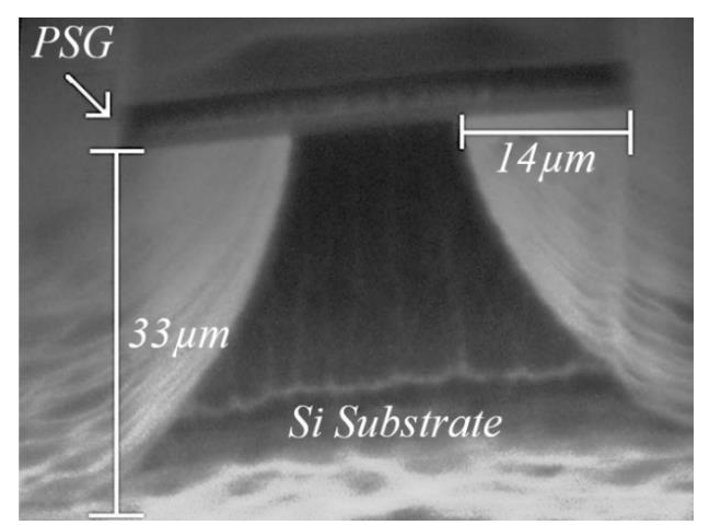
The PolyMEMS® fabrication process begins with the growth of silicon oxide 2000 Â at a temperature of 1000 °C; then a deposition of 0.5 μm undoped polysilicon by LPCVD at 650 °C. Phosphorus Silicate Glass (PSG) film of 2 μm thick is deposited by APCVD (Figure 1a). Using one lithography mask to etch the PSG and open windows, the anchoring of structures is conducted. The PSG is etched by RIE dry etching with CF4. The masking used is the AZ - 2070 negative photoresist (Figure 1b). The polysilicon deposition is performed by LPCVD at 650 °C, the film is n+ doped with Phosphorus at 1000 °C; the thickness deposited are 1, 2 and 3μm in different samples (Figure 1c). Using the mask 2, the test structures are defined by dry etching in RIE. The gases used are SF6 and O2 in a ratio of 1.5:1. For masking a SiO2 film of 2000 Â is used (Figure 1d). A 1000 Â film of aluminum is then deposited (Figure 1e). The lithography for the aluminum is conducted using mask 3. This film is used as electrode material and to improve the mechanical stability of the anchored material. The aluminum is etched using a wet process with Al-Etch (Figure 1f). For releasing the structures, the last step is the removing of sacrificial material (PSG). By the use of mask 3, a 2 μm of photoresist film is the protecting material to avoid the etch of aluminum during the sacrificial etch. The release step is performed by wet etching process in a 49 % HF solution. A series of alternating washes of isopropanol, DI water and isopropanol is performed to remove HF residues. Finally, the samples are dried in a convection oven at 120 °C. Figure 2 shows a cross section of a microstructure using the PolyMEMS® fabrication process.
B. CMOS Technology Module
The CMOS module is under development with the purpose of fabricate electronic circuits with 3 μm length as minimum feature and ± 5 supply voltage. For matching the threshold voltage transistors, a twin-well diffusion and latch up-free structure were used [7]. In addition, the CMOS process uses a self-aligned titanium silicide-polysilicon gate, which also serves as local interconnect, polysilicon and aluminum for interconnection. These different interconnection levels are enough to obtain and to ensure the required intercommunication without an increase in difficulty or cost. In Figure 3 the CMOS process steeps designed represented in schematic form are shown [10]. The CMOS module consists of 9 masks and 12 lithography steps. The main blocks are briefly discussed in the following: Initially the formation of the N- and P- wells, as twin wells, are ion implanted and the drive-in thermal diffusion is performed at 1200 °C. The junction depth (3.5 μm) is designed to be deep enough to avoid vertical punch-trough. The active areas are defined by using Poly buffered local oxidation of silicon (PBLOCOS) for a precise feature definition.
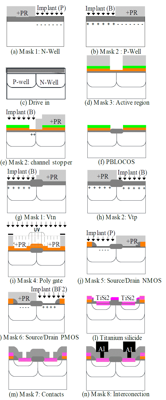
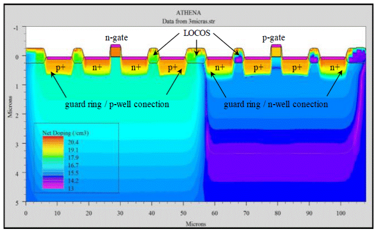
A p-channel stopper is used to reduce the spacing between devices and providing better isolation. A 200 Å gate oxide is thermally grown at 900 °C in dry oxidation. 400 nm of Poly films are low-pressure chemically vapor-deposited (LPCVD) at 650 °C, after that a 1000 °C phosphorus doping is performed during 30 minutes. This process is designed with shallow source/drain junctions (0.7 μm) as well as low gate and drain/source sheet resistances to minimize the delay and increase the current drive of the devices. The titanium silicide (TiSi2) electrodes are defined using a self-aligned process realized at 900 °C in nitrogen ambient. A precise low-dose of boron ions is implanted for threshold adjusting of CMOS transistors. Interconnecting aluminum film is deposited and patterned, and finally a 450 °C sintering is performed. The main process specifications are summarized in Table 1. Figure 4 shows a cross section for the CMOS architecture obtained from a simulation of the process using the Athena environment from SILVACO® suite [11]. The process is designed with a first alignment mask process (not illustrated) to correctly align the subsequent photolithography steps.
Table 1 CMOS Module specifications
| Parameter | Symbol | Value |
|---|---|---|
| Threshold Voltage N/P channels | Vto | 700 mV |
| Gate Oxide Thickness | Tox | 200 Å |
| N-Well Depth | Xnwell | ~ 3.5 μm |
| N-Well Surface Concentration | Nnwell | ~ 4.5 x 1015 cm-3 |
| P-Well Depth | Xpwell | ~ 3.5 μm |
| P-Well Surface Concentration | Npwell | ~ 9 x 1016 cm-3 |
| Poly Gate thickness | Tg | 0.4 μm |
| Source/Drain Junction Depth | Xj | 0.7 μm |
A Monolithically Integrated MEMS Technology
The monolithic integration is performed in a single wafer which includes circuits and microstructures. A classification of the step process with several materials and chemical ambient must be correlated with some type of MEMS integration: Post, Pre, and Intra-CMOSapproaches [12-14].
The PolyMEMS INAOE® technology has a thermal budget limited to 1000 °C, and according to the CMOS thermal budget shown in Figure 5, a Pre-CMOS approach is unsuitable due to the eventually long time increment required to adjust the twin-well drive-in from 1200 °C to 1000 °C. A Post-CMOS approach using the current PolyMEMS INAOE module cannot be compatible due to the requirements for the LPCVD Poly films, which are doped and thermally annealed at 1000 °C for a time longer than 30 minutes. Given the above considerations, as alternative we focus on the Intra-CMOS integration, keeping safe the CMOS module, since the INAOE has its own facility for device fabrication, adapt and optimize the required process flow to minimize both electronic and mechanical degradation in accordance with the thermal budget.
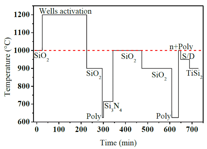
Figure 5 Thermal budget for 3 μm CMOS process. The dashed line limits the allowed temperature for fabrication process of microstructures for an intra-CMOS approach.
A. thermal Analysis on CMOS Process Design
In the developing of a practical intra-CMOS process, it is necessary to consider that the CMOS module is extremely sensitive to thermal treatments than the polysilicon microstructures. Because the goal is the integration of these different fabrication modules, a thermal study related with dopant profiles is required. For the analytical study, all the CMOS doping profiles was considered resulting in a wide range of overall annealing time to be included. Simulation routines were performed using Athena and Atlas environments from SILVACO®, in which the tuning of all the modules was performed with the data obtained from the characterization of the 3 μm CMOS technology developed.
For example, the final part of the CMOS module is designed with a silicon/silicide interface for electrical interconnection, which imposes limitations to the post thermal cycles to a 900 °C maximum range, for avoiding structural interface damages due to titanium silicide (TiSi2) reactivity [15]. On the other hand, at the initial part the P/N wells drive-in require a 1200 °C annealing temperature. At this high range temperature, we have identified a breaking step, where the CMOS sequence could be interrupted as a secure practical way to avoid undesirable post-thermal side effects on the CMOS architecture. The overall mechanical module may be fabricated after P/N well annealing and ending with the rest of CMOS steps without affecting the overall sequence.
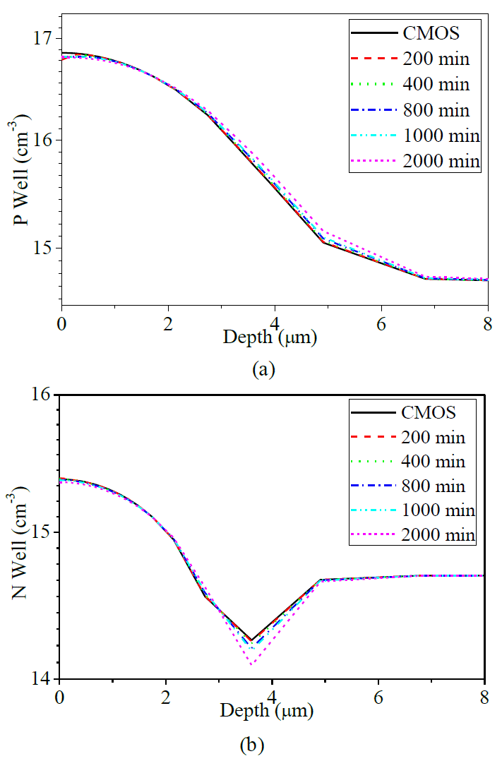
A thermal simulation was performed to demonstrate the invariance and robustness of the P/N wells after a long annealing time at 1000 °C as that required for the microstructure fabrication. Figure 6 shows the simulated post-annealing effect on the P/N wells after 200, 400, 800, 1000 and 2000 minutes of thermal annealing under nitrogen ambient at 1000 °C. From the Figure 6 can be observed that P-well and N-well show a 3.5 - μm junction depth after 1200 °C annealing. From Figure 6 it can be seen that both impurity profiles remain almost unchanged with annealing time; also the annealing time was set with the intention to demonstrate that any type of microstructure, that may require a very long annealing time at 1000 °C, could really be considered. The most significant issue observed after the very long post-annealing treatments, was a slight surface concentration variation at both wells, which is due to boron and phosphorus segregation at both wells/capping oxide interfaces [16].
B. Trench for Microstructures
The way for the electronic-mechanical coupling is another key step in the design of the integrated process. Figure 7a shows the step height h of some poly-microstructure facing the surface CMOS diffusions. It can be observed the high aspect ratio of the microstructures. In the intra-CMOS approach, the microstructures will be fabricated before completing the CMOS steps, this means the CMOS photolithography steps will be affected by the height of the already defined microstructures.
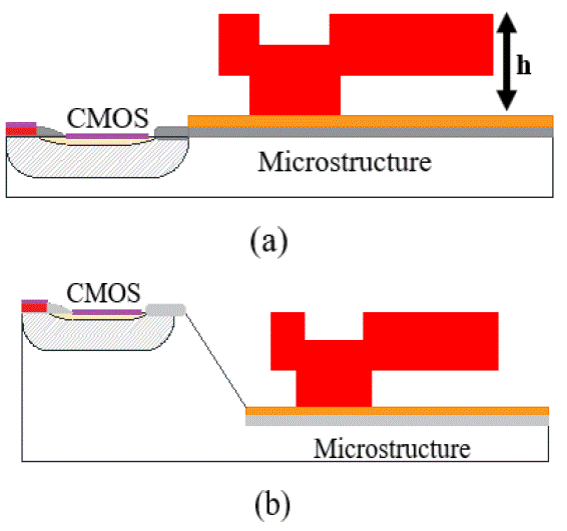
Figure 7 (a) Schematic of an integrated microstructure besides surface CMOS diffusions showing the resulting aspect ratio differences, (b) Cross section of the generic integrated MEMS process here proposed.
It is well known that CMOS features are directly affected by some process variations like misalignments, film thickness variations due to deposition techniques or step coverage. Our integration approach is designed to be developed without some planarization technique; hence the microstructures depicted in Figure 7(a) will cause some lateral size shift during the photolithography steps for developing the CMOS devices.
In our proposed approach, we are considering the case when the microstructures are placed inside a shallow trench. In a general trace, Figure 7(b) shows a graphical representation for this approach; the trenched microstructures result uncritical for the minimum feature definition, considering the subsequent CMOS photolithography steps and the final interconnection with the microstructures. The depth of the trench is directly related with the specific microstructure arrangement but is no deeper than 6 microns. We are using P-type and (0 0 1) silicon wafers, hence when the shallow trench is etched with aqueous Tetramethylammonium hydroxide (TMAH) the of four-fold symmetry wall-sloped allows the deposition interconnecting stripes.
Considering general aspects for a trench some morphology requirements must be carefully considered. In our approach without planarization step, the presence of material stacking around the trench complicates the subsequent photolithography process but also results more difficult to define geometries over the PSG at the bottom of the trench. To compensate the lack of planarization step we propose the use of an extra fabrication mask to etch the materials around the trench. By using this extra mask, the height h will disappear and both the CMOS and microstructure definition become easier.
C. The proposed Generic and Modular Monolithic Integrated MEMS Process.
Figure 8 shows the fabrication steps, obtained using the Athena environment, of the entire integrated MEMS process designed. This monolithic integrated MEMS fabrication process is divided into four main sections; the entire fabrication sequence is carried out with 13 masks and 16 photolithography steps in a p-type (1 0 0) silicon wafer (Figure 8a):
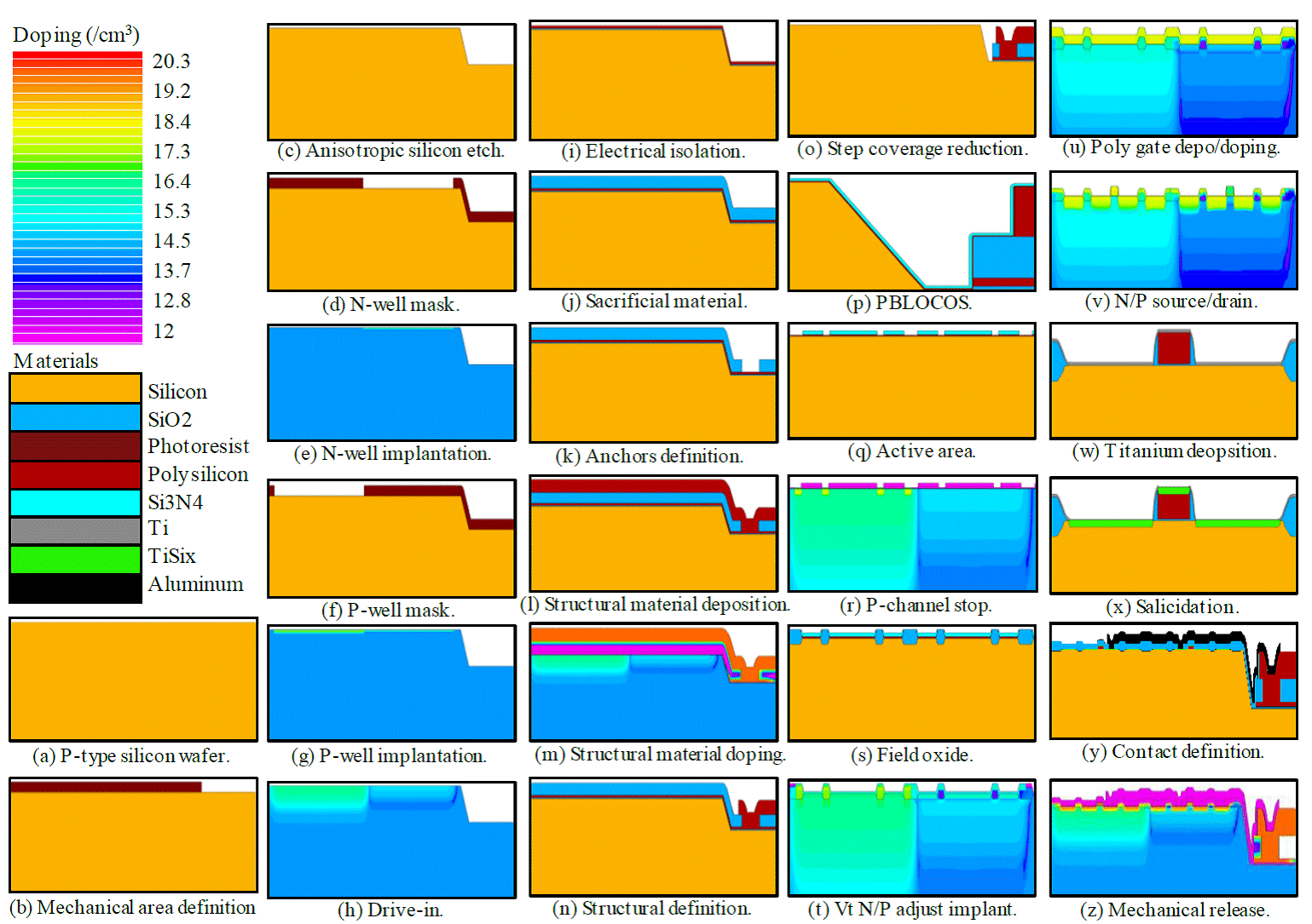
1) CMOS Part I: The process starts with an initial thin oxide (~ 200 Å) to define the alignment marks and then the trenches are defined by using aqueous TMAH solution for CMOS compatibility. Low dose ion implantation for P and N wells and immediately a thermal drive-in at 1200 °C is performed in nitrogen ambient during 200 minutes. These steps are listed below:
Process Step:
1. Initial Oxidation, T = 1000 °C, dry O2, Tox = 20 nm.
2. Mark alignment and TMAH silicon etch at 60 °C, using the initial oxide as masking material (Figure 8b)
3. Phosphorous implantation, Dose = 6.5 × 1010 cm-2, (N-well). Energy = 100 KeV (Figure 8d,e).
4. Boron implantation, Dose =1.5 ×1013 cm-2, (P-well). Energy = 80 KeV (Figure 8f, g).
5. Drive-in at 1200 °C, 200 minutes, N2 ambient (Figure 8h).
6. Etching of initial oxide.
2) Polysilicon Microstructures: An insulator film is deposited for electrical isolation between the microstructures and the surface wafer. Then a sacrificial material is deposited followed by the deposition, doping and patterning of the structural material inside the trenches. A thermal treatment is realized at 1000 °C to minimize the residual stress.
Process Step:
7. Thermal oxide, T = 1000 °C, Tox = 0.3 μm, (Figure 8i).
8. LPCVD intrinsic polysilicon, T = 650 °C, Tpoly = 0.5 μm, (Figure 8i).
9. Sacrificial oxide deposition, Tox = 3.0 μm, (Figure 8j).
10. Structural material deposition, Tox = 2.0 μm, (Figure 8I).
11. Thermal annealing and doping at 1000 °C, t = 120 minutes in N2, (Figure 8m).
12. By the use of an additional mask, the material outside the trench is etched, (Figure 8o).
3) CMOS Part II: The After the complete definition of the microstructures, the CMOS process sequence is realized in the top surface of the wafer. The standard PBLOCOS CMOS process is realized and the microstructures remain covered by the stacked materials from the local oxidation process. Field oxidation has a thermal cycle of 1000 °C for 2 hours, and serves as a stress reduction thermal cycle for the microstructures. The following fabrication sequence is listed below.
Process Step:
13. PBLOCOS. Deposition of a stacked silicon dioxide, polysilicon and nitride films. This step protects the microstructures, (Figure 8p).
14. Active area definition, (Figure 8q).
15. Channel stopper implantation, (Figure 8r).
16. Field oxide growing at 1000 °C. Tox = 0.58 μm, t = 2 hour, (Figure 8s).
17. VTn boron adjust implantation, (Figure 8t).
18. VTp boron adjust implantation, (Figure 8t).
19. Gate oxide T = 900 °C, Tox = 20 nm, (Figure 8u).
20. LPCVD Gate Poly, Tpoly = 400 nm, (Figure 8u).
21. Poly phosphorus doping at 1000 °C, 10 Ω/□, (Figure 8u).
22. Source/Drain implantation, (Figure 8v).
23. Dopant activation at 950 °C, (Figure 8v).
24. Titanium deposition and self-aligned silicidation at 900 °C, (Figure 8w, x).
4) Interconnections and Releasing: The passivation layer is deposited to protect both the CMOS and microstructures devices. The interconnection between the CMOS and the microstructures is carried out in the metallization step by using a sputtered aluminum film to ensure proper step coverage from the top of the wafer (CMOS area) to the bottom of the trench (microstructure area). The final step in the fabrication process is the sacrificial etch to release the microstructures (Figure 8z). The last etching process depends on the specific microstructure geometries, and it can be done by some dry or wet etching technique.
Process Step:
25. Passivation film deposition, (Figure 8y).
26. Aluminum deposition and patterning (simultaneous interconnection), (Figure 8y).
27. Sintering at 450 °C (gas forming)
D. Simulation Results
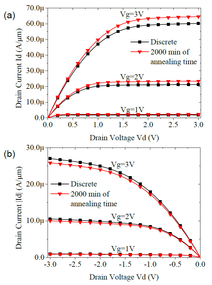
Figure 9 shows a cross-section of the simulated MEMS fabrication process; inside the trench are the main devices for this technology. The modeled and simulated transistors have a length of 3 μm (minimal dimension), and the current in all the sirnulations is norrnalized to a width of 1μm.Figure 10 shows the simulated drain current (I d ) versus gate voltage (V d ) curves for both types of transistors; the behavior of transistors was obtained at V d = 100 mV with an interface charge of 5 × 10¹⁰ C/cm2.The change in I d current after annealing of the devices at 1000 °C at different period of time. It can be seen that I d -V d characteristics of the transistors remain almost unchanged, indicating their robustness to the intra process fabrication of the micromechanical structures. In order to demonstrate the robustness of the CMOS process to the thermal treatments needed for completion of the MEMS fabrication, Figure 11 shows the impact of the annealing time on the threshold voltage of the devices. Figure 12 shows the simulated drain current (Id) versus drain voltage (Vd) curves at different gate voltage, for discrete transistors and after 2000 minutes of annealing time. The slight variations for the drain current Id are corresponding with the graphs shown in the Figure 10 and Figure 11, such Id variations are attributed to the slight variations on the surface dopant concentration of the P/N wells/oxide interfaces previously analyzed in Figure 3. The overall result is that the CMOS devices and microstructures can be fabricated on the same substrate with minimal variation in the electronic-mechanical performance even after 2000 minutes of annealing time.
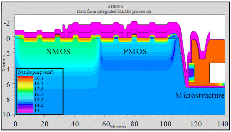
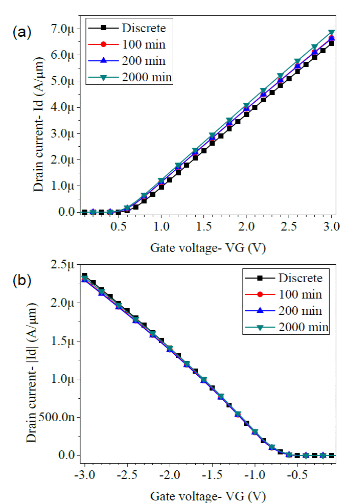
Figure 10 Simulated V g vs. I d curves for transistors, after three additional thermal cycles: (a) NMOS transistor and (b) PMOS transistor. The gate length of the transistors was 3 μm.
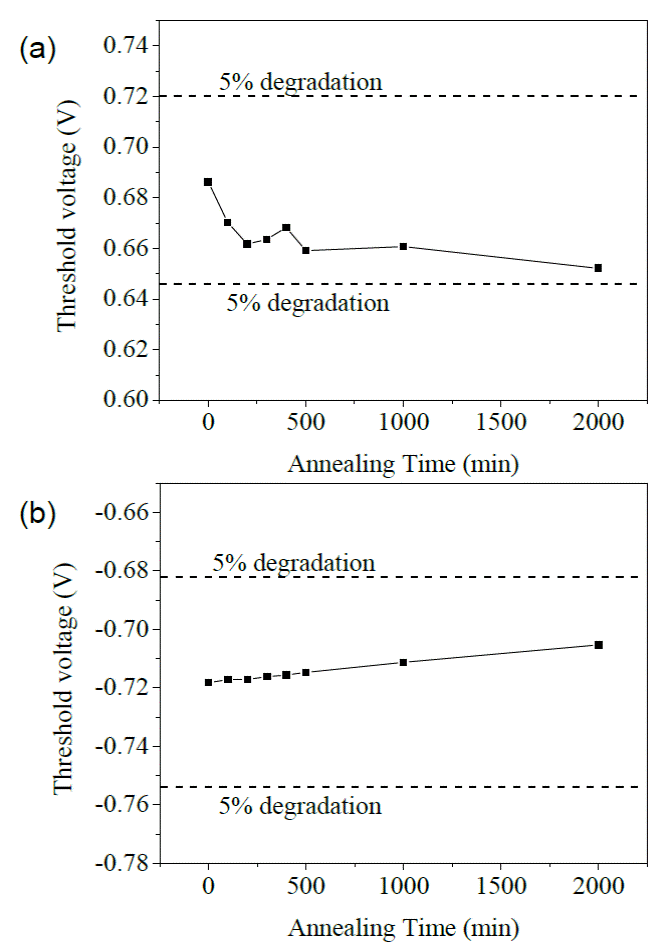
Figure 11 Threshold voltage variation on transistors after annealing time at 1000°C. (a) NMOS transistor and (b) PMOS transistor.
The Test Chip
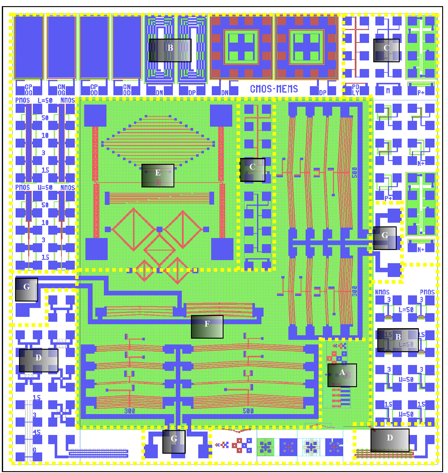
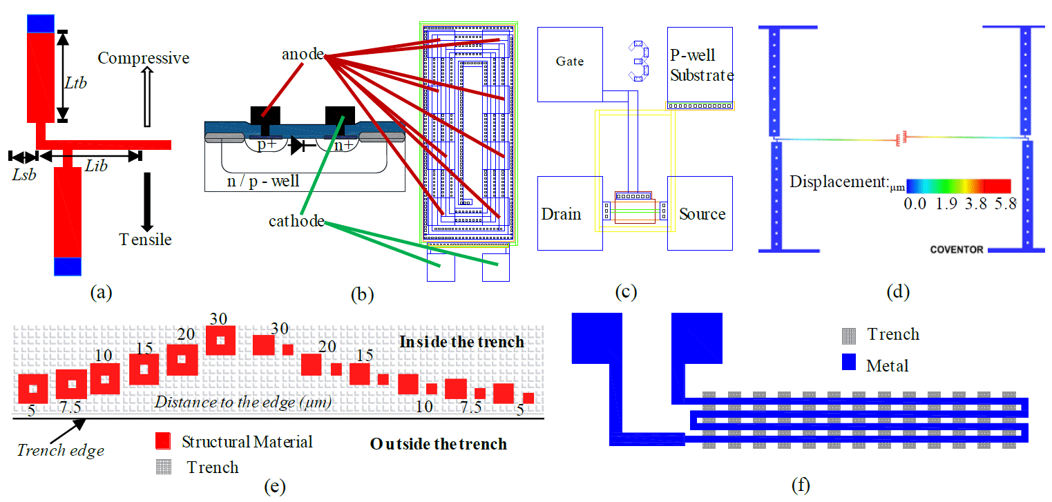
A test chip was designed to evaluate and assist the development of the generic and modular integrated MEMS process proposed. This test chip will be useful for identifying the possible electrical and/or mechanical variations on the material properties and devices performance due to the fabrication process. Figure 13 shows the layout of the designed test chip. The chip size is 4.3 × 4.2 mm, and in it all the CMOS devices surround the mechanical structures. All test structures use a 2 × 5 terminal array module to facilitate the testing process at wafer level.
Design considerations of the test chip
In the test chip, all the CMOS devices surround the mechanical structures since they are always affected by external and internal stress and their location on the die is critical to guarantee the optimal performance of the designed device. A brief analysis about the stress is described below.
Usually the mechanical structures are tested at a wafer level and the residual stress is produced during the fabrication process. However, the technique required to attach the die to the package (adhesive, wire bond, molding compound), may apply stress gradients to the entire wafer [17,18]. As the mechanical structures are stress sensitive components, it is convenient to locate them near the center of the die where the induced stresses are more uniform [19], [20]. It is clear from the above that the design must include all the mechanical structures at the center of the die.
A 2 × 5 probe pad array [6], [21], is used in the design of the test structures to facilitate the test process by employing standard probe cards. Also, the use of a 2 × N probe pads arrangement, allows the test pads to be an integral part of the test structures, to avoid having common buses among the test structures to prevent the interference between different structures, and to obtain the highest degree of modularity.
The designed test structures are classified into four categories: CMOS test structures, Mechanical test structures, Interconnection reliability test structures and Functional micro-actuators, and they are distributed in modules into the chip. The test chip includes the following modules (highlighted in Figure 13): A) Fabrication test structures checked during processing; B) Devices test structures (MOSFETs, capacitors, diodes); C) Process test structures (sheet resistance, contact resistance); D) Interconnection reliability test structures (continuity, sheet resistance inside the trench); E) Stress monitors (buckling structures, rotating structure); F) Micro- actuators (chevron arrays); and G) Wiring pads (to wire the micro-actuators). Detail of some mechanical and electrical test structures are shown in Figure 14.
Conclusions
A generic and modular design approach for a monolithic MEMS process is proposed without specialized planarization techniques. The integration is realized with CMOS devices and polysilicon microstructures. From the simulation results a non significant degradation on the CMOS performance devices is observed after MEMS fabrication. The intra-CMOS process approach showed to be the best approach for a modular design of a MEMS fabrication process at the LIMEMS-INAOE. The thermal budget of the modules plays a crucial role, because it set the conditions for obtaining the complete set of devices fabricated near their optimal point, that is, without degradation of current handling and without V to shift in the CMOS process and with the minimum residual stress on the micromechanical devices.
A CMOS-MEMS test chip for the evaluation during both process development and fabrication was designed. The test structures provide optical and electrical information about the material properties to study the feasibility of the integration of CMOS devices and mechanical structures.
The use of the 2 × 5 probe pad array will improve the electrical measurements to perform statistical analysis. Polysilicon and aluminum were the base materials in the mechanical design of the test structures; nevertheless, another materials with Young modulus near the range of the mentioned materials, like silicon-germanium, amorphous silicon, even copper can be selected to fabricate the mechanical structures, and the same design will be enough to characterize the residual stress in the films. The information obtained from de test chip will be useful for tuning simulation routines and analytical expressions. Then, the developing of a new integration technology is supported. The fabrication process of the designed test chip is still in progress during the preparation of this paper.

