


 nova página do texto(beta)
 Inglês (pdf)
 Artigo em XML
 Referências do artigo
 Enviar este artigo por email
 Citado por SciELO
  Similares em
SciELO
Similares em
SciELO 
 Permalink
Introducción
Polydimethylsiloxane (PDMS) is a polymer which is often used for microfluidics and bioMEMS applications. It has many advantages over other materials used in microfluidic assays such as glass or silicon. PDMS is flexible, impermeable to water, non-toxic to cells but is however permeable to gases [1], biocompatible, which makes it very attractive for biological application [2]; it is an inexpensive material and it is easy to use for microfluidic devices fabrication [3-6], from very complex systems to simple but useful forms.
During the fabrication of PDMS-based devices, patterning, molding, curing and bonding are the major steps that define the performance of the device [7-9]. In the molding step, PDMS is patterned from the soft lithography process, when poured over a mold made from negative photoresist [10,11], usually SU-8, or through an etching process [12]. The patterned PDMS completes the desired microfluidic device when it is bonded to a suitable substrate.
At present, there are several methods to bond PDMS surfaces. The plasma assisted process is the most commonly used method, typically from oxygen plasma which produces hydrophilic silanol PDMS surface groups, allowing irreversible bonding between two fully cured PDMS structures [13,14].
Some other methods rely on an adhesive layer to bond the surfaces, like the curing agent that is used for PDMS synthesis [15]. The 'stamp-and-stick' approach, using an intermediate layer of uncured PDMS, is employed also as a method to bond layers together [16]. The main objective of all these methods is to achieve the best union between the PDMS surfaces. However, they can show inconsistent bonding results, which cause leakages and improper performance of microfluidic devices.
In this work, we describe a different molding and bonding method in order to obtain a reliable union between PDMS layers, intended to eliminate defects on the interface that are unwanted for microfluidic applications. We show a comparison between bonding methods reported in the literature and the method proposed in this work, evaluating the interface for each method from scanning electron micrographs (SEM). The presented method has resulted in minimal interface defects, suitable for fabrication of membranes, micro pumps, valves, mixers and other structures [17,18].
Methods used to bond PDMS layers
The structure used for the assessment of PDMS bonding methods consists of a PDMS substrate with a thickness of 3 mm supporting a thin PDMS membrane, 95 μπι thick. Both of the separated PDMS layers are prepared according to the manufacturer instructions (Dow and Coming's Sylgard 184, thoroughly mixed at a ratio of 10:1 PDMS base:curing-agent (catalyst)).
In order to compare our bonding technique with respect to the other methods, sample structures were prepared according to the reported techniques. For the first sample, the separate layers were fabricated as follows: one portion of PDMS mixture is poured on a photoresist-covered silicon wafer and spun for 60 seconds at 800 rpm, obtaining a membrane 95 μm thick after curing at 70 °C for 2 hours. To obtain the substrate, a mold is placed on top of a photoresist-covered silicon wafer, the PDMS is poured inside the mold and then placed in a 70 °C oven for 2 hrs. When cured, the separate layers are placed in a Reactive Ion Etcher (RIE) system and processed for 10 minutes in oxygen plasma at 20 W in order to produce hydrophilic silanol at the PDMS surfaces. Then the exposed surfaces were pressed together and put in an oven at 70° C for 15 minutes to promote the adhesion.
The next sample was prepared as before, molding and curing two separate layers. The substrate was bonded to the thin membrane still attached to a silicon wafer using the ‘stamp-and-stick’ approach. In this case, a small amount of PDMS mixture was spun over a clean silicon wafer to obtain a thin uncured PDMS layer. Then, the cured PDMS substrate was stamped over this layer, retired and stuck over the thin PDMS membrane without oxygen plasma treatment. Thus, the complete structure was put in an oven to cure. The uncured PDMS layer serves to adhere the two surfaces together.
For the third method tested, the separate layers were fabricated as mentioned before, then a thin layer of catalyst was deposited on the fully cured PDMS membrane fixed on a silicon wafer. The remaining substrate was set over it and put into the oven to cure. In this last bonding method, the catalyst acts as the adhesive layer.
Finally, the presented bonding method consist, as described before, in pouring one portion of uncured PDMS over a photoresist-covered silicon wafer and spun for 60 seconds at 800 rpm, in order to obtain the 95 μm thick membrane. After curing at 70°C for 2 hours and oxygen plasma treatment (10 minutes @20 W), the corresponding mold is placed onto the cured membrane and a batch of PDMS mixture is poured over the mold and set to cure again at 70 °C for 2 h to form the substrate. In this case, a complete part of the structure, i.e., the substrate, is molded after the oxygen plasma treatment. This critical step achieves the silanization of the cured PDMS membrane surface and promoting the interaction with the uncured PDMS to obtain a seamless, monolithic structure. Lastly, for all cases, the mold is retired and the final structure is released from the silicon wafer using an acetone lift-off process, in order to free the PDMS structure from the silicon wafer; and the samples cut in half for interface analysis by Scanning Electron Microscopy (SEM).
Results and Discussion
Figure 1 shows the interface between two fully cured PDMS surfaces from the bonding method using oxygen plasma. This interface shows some defects which are related to the air pockets generation between the surfaces, surely producing leakages in the microfluidic structures.
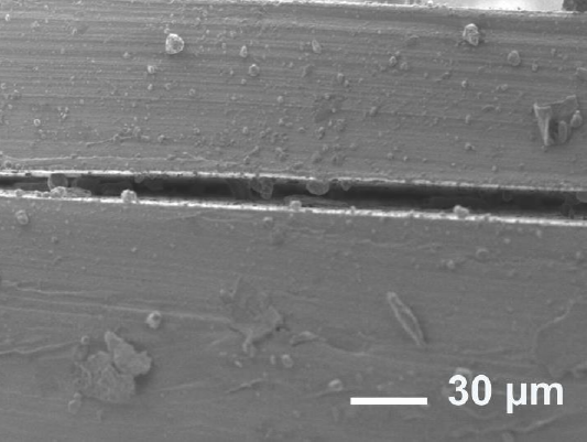
Figure 1 SEM image of defects on PDMS interface bonding using oxygen plasma showing the separation of PDMS surfaces failing to bond.
The overall adhesion of the surfaces presented problems, only achieving good bonding where the surfaces were together for an amount of time. Due to the elastic nature of the material, in some places the surfaces tended to remain separated, therefore preventing bonding. With this method, the thin layer could be separated easily from the substrate.
This bonding method also shows that any debris on the surface can produce a gap or an air pocket, as seen in Figure. 2, caused by the elastic nature of cured PDMS as well. The formation of several small air pockets was evident again in the 'stamp-and-stick' approach.
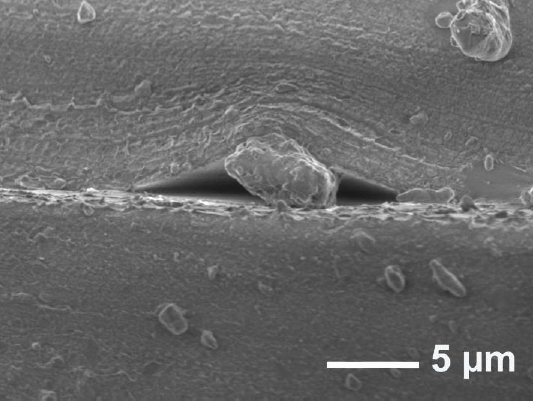
Figure 2 SEM micrograph of debris on PDMS interface bonding using oxygen plasma showing trapped debris between PDMS surfaces forming voids.
The SEM interface characterization in this case is shown in Figure 3. As with the first method discussed in this section, the elasticity of the material prevented the bonding over the complete surface of the sample causing small air pockets, however the interface between the bonded surfaces is satisfactory where the liquid PDMS layer adheres to both surfaces as indicated in Figure 3.
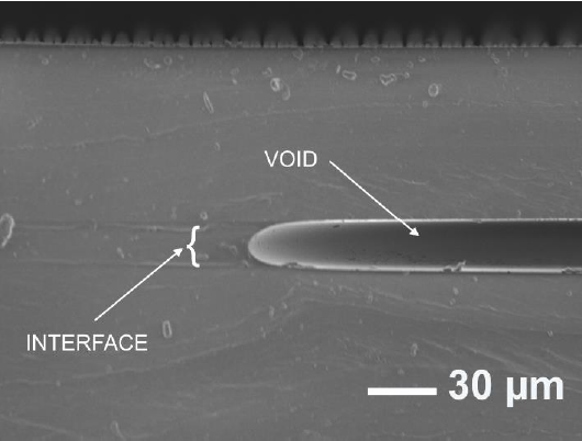
Figure 3 SEM interface image of two cured PDMS from 'stamp-and-stick' method showing a void between the PDMS surfaces.
It appears that this strategy requires a way to hold down the two parts to ensure a complete bonding and avoid air pockets in the interface. With this method, the thin layer could not be separated from the substrate without rupturing.
The interface formed in the sample prepared with catalyst as adhesive is shown in Figure 4. This sample had zones where the two layers were not bonded. The thin layer could be separated from the substrate with little force, indicating that the adhesion was not as effective as the other techniques. The interface is clearly visible, with thickness of about 15 microns between the two solid PDMS parts. This technique shows some minor bubbles that can be problematic when fabricating microfluidic systems.
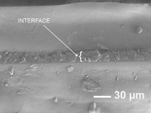
Figure 4 SEM micrograph of interface of two cured PDMS by using catalyst as an adhesive layer, showing the interface formed.
These last bonding methods, which use an adhesive layer, showed slippage during the bonding PDMS surface when the curing of adhesive layer was carried out in the oven.
In this case, the liquid adhesive was serving as lubricant, thus the thick PDMS substrate was displaced from the original position. This effect can be minimized leveling any supporting rack and using a mold to hold the parts in place. Nevertheless, this slippage permits the aligning of parts in a multilayer system.
A drawback of the three techniques described and tested before is that they are somewhat dependent on the geometry of the intended structure, as if the surface is not completely flat, voids will surely appear. Also, the cleanliness of the surfaces is also a concern, as the voids can be caused by foreign objects. Nevertheless, the methods that rely on an adhesive layer have a very important advantage, in that they do not need a plasma treatment, which could be not ready available.
The bonding method reported in this work presented an interface free of defects, with a minimum thickness. The interface formed by the PDMS membrane and the PDMS substrate is shown in Figure 5, noting that the interface is minimal. The marks in the membrane are caused by the cutting process.
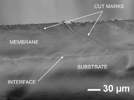
Figure 5 SEM image of two PDMS surface bonded with the proposed method in this work, showing the minimal interface.
The presented bonding method exhibits several advantages. In this case, the two PDMS structures are bonded together as part of the molding process, as such, is does not show any zones where the interface fails. Also, any debris found on the substrate becomes encapsulated completely by the liquid PDMS, minimizing the effect this debris could have. Aligning different parts is not an issue; instead, the aligning must be performed on the molds and other patterns to ensure the desired result.
The microfluidic systems sometimes require integrating other materials into the substrate, as sensors or actuators but in most cases, it is not possible. However, the presented method can achieve a solid integration or encapsulation of foreign materials into the PDMS structure, most notably, the integration of inlet and outlet ports in the microfluidic device.
A non-desirable effect of bonding methods which use an adhesive layer is that the dimensions and geometry of the completed microchannel can be altered due to the liquid bonding layer, as it introduces into the molded channels, even blocking it if the process is performed incorrectly.
This method was carried out to fabricate PDMS diaphragms intended to be used in pressure sensors and as reservoir for drug dispensing systems; therefore, a complete bonding between the surfaces that define the structures must be accomplished.
Figures 6(a) and 6(b) show scanning electron microscope photographs of diaphragms for 500 μm and 95 μm thick respectively, where the monolithic quality of the structure can be seen.
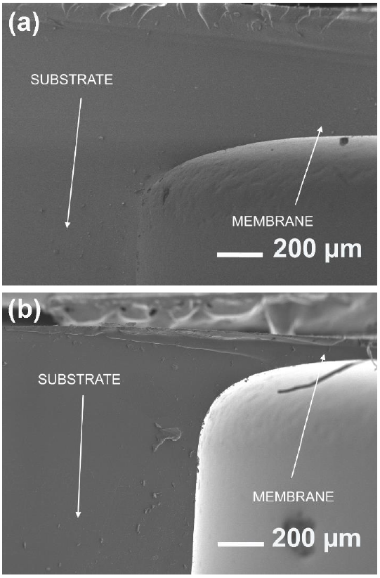
Figure 6 Cross section SEM images of diaphragms fabricated using the proposed bonding method for (a) 500 μm and (b) 95 μm thick.
It is worth noting that the fabricated structures are thoroughly integrated such that no interface was exhibited, thus the membrane cannot be separated from the substrate without rupture.
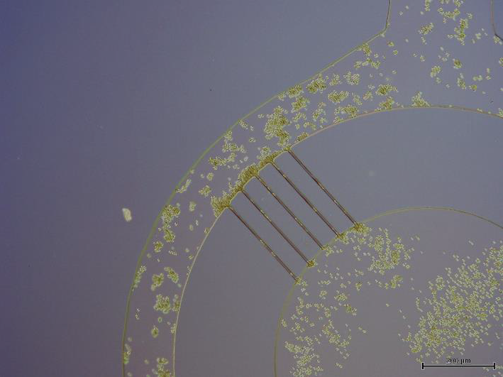
Other devices were fabricated using this method to complement soft lithography fabrication of microfluidic assemblies, such as cell filters.
Figure 7 shows a detail view of microchannels from the bottom of the PDMS cell filter, after the first fabrication step, molding with soft lithography. At this stage, the fabrication process requires the proposed method for bonding the PDMS surfaces. The photograph in Figure 8 shows the completed cell filter under testing, fabricated completely with PDMS.
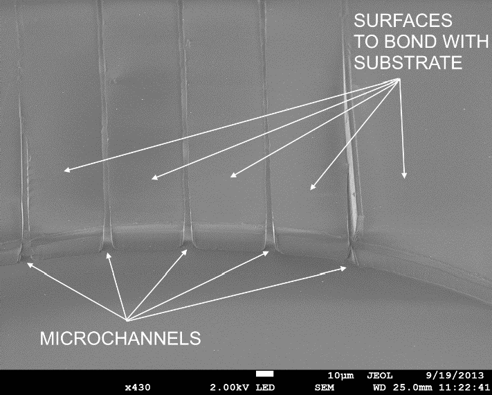
Figure 7 Bottom view of a PDMS cell filter fabricated with soft lithography before completion with the presented method to bond PDMS layers.
Conclusion
A method to bond surfaces of PDMS is presented. This method relies on the oxidation of the fully cured PDMS surface and the interaction with the uncured PDMS preparation to ensure a defect-free interface.
The presented liquid PDMS bonding permits the introduction of foreign materials, structures and devices and encapsulates them without the need of extra molding, punching or carving of PDMS. Furthermore, the proposed bonding method allows bonding not only thick layers of PDMS but also thin layers of less to 500 μm which are difficult to handle at these thicknesses.
The comparative of proposed bonding method with respect to the other previously reported bonding methods approves that the quality of the interface is improved, suitable for microfluidic applications where leakage and detachment of the layers is undesirable.

