


 nueva página del texto (beta)
 Inglés (pdf)
 Artículo en XML
 Referencias del artículo
 Enviar artículo por email
 Citado por SciELO
  Similares en
SciELO
Similares en
SciELO 
 Permalink
Introduction
Although the requirements of a material for biomedical applications as coatings for implants [1] or implantable devices [2] are different of those for biological applications as cell culturing [3], tissue regeneration [4] and biosensors [5], there are two properties in common: biocompatibility and no cytotoxicity. A biocompatible material must be chemically stable and must have low dissolution rate in biological medium to avoid any adverse reactions, whereas a no cytotoxic material is not toxic to cells [6]. Undoubtedly, the development of these properties by a material is closely related to the elements that are part of the material and the chemical bonds between them, which result in the material structure. Materials to be included into devices must be obtained under compatible conditions with the fabrication processes of the devices. Furthermore, the properties of the materials must be in accordance with its specific role into devices [7]. For all these reasons, the success of a material in an application depends on the correct definition of the mechanism and the parameters to obtain it.
According to previous published works [8], hydrogenated amorphous silicon carbon alloy (a-SixC1-x:H) is a candidate for biomedical and biological applications, among other reasons because its chemical structure is based in chemical bonds of silicon, carbon and hydrogen. In this work plasma-enhanced chemical vapor deposition (PECVD) is used to obtain a-SixC1-x:H films with a narrow range of deposition parameters considering these applications. Furthermore, a study on the influence of methane-silane gas flow ratio (XCH4), hydrogen dilution and doping level on the morphology, the formation of Si-C bonds, and the optical and electrical properties of the films is addressed.
Experimental
The deposition processes of a-SixC1-x:H films were carried out in a ultra-high-vacuum multi-chamber PECVD system (MVSystem Inc.), which operates at a radio frequency of 13.56 MHz. All a-SixC1-x:H films were deposited with precursor gases of silane (SiH4) diluted at 10% in H2 and methane (CH4), onto 2947 Corning glasses, p-type silicon substrate (100), and titanium stripes on glasses. Hydrogen (H2) was used as a carrier and diluent gas. Taking into account that the compatibility of the deposition process with the Si-based microfabrication technology and the applications increases when low deposition temperatures are used [2,7], temperatures of 150 °C and 200 °C were selected. To obtain carbon-rich films, methane-silane gas flow ratios (XCH4) of 0.70 and 0.85 were chosen. According to Iliescu et al. [3], under high pressures the films obtained have good uniformity, then the pressure was set to 1.5 Torr. Under low deposition power density, the deposition process is controlled by the reaction of silane radicals with methane molecules, making the deposition more orderly [9]. Two power densities of 25 mW/cm2 and 50 mW/cm2 were defined to achieve this effect.
Two hydrogen dilution (ZH2) of 2.7 and 9 were set to study its influence in the material properties. Finally, some films were doped from 0.5% to 2.5% using diborane (B2H6) as dopant gas (B-doped a-SixC1-x:H films). All the deposition processes are shown in Table 1.
Table 1 Deposition parameters of the PECVD processes, and deposition rate, root-mean square roughness (Rq), density of Si-C bonds (NSiC), density of C-H bonds (NCH) and density of Si-H bonds (NSiH) of undoped and B-doped a-SixC1-x:H films.
| PECVD process |
XCH4 | ZH2 | YB (%) |
Power density (mW/cm2) |
T (oC) |
Deposition rate (nm/min) |
Rq (nm) |
NSiC (bond/cm3) |
NCH
(bond/cm3) |
NSiH
(bond/cm3) |
|---|---|---|---|---|---|---|---|---|---|---|
| aSiC-01 | 0.7 | 2.7 | 0 | 50 | 150 | 11.17 ± 0.16 | 2.33 ± 0.34 | 2.09×10²¹ | 1.16×10²² | 4.69×10²¹ |
| aSiC-02 | 0.7 | 9.0 | 0 | 50 | 150 | 7.65 ± 0.05 | 1.00 ± 0.09 | 1.54×10²¹ | 1.60×10²² | 4.08×10²¹ |
| aSiC-03 | 0.85 | 2.7 | 0 | 50 | 150 | 11.95 ± 0.12 | 0.88 ± 0.02 | 1.10×10²¹ | 1.34×10²³ | 2.96×10²¹ |
| aSiC-04 | 0.85 | 9.0 | 0 | 50 | 150 | 6.29 ± 0.01 | 0.88 ± 0.21 | 1.78×10²¹ | 1.67×10²² | 3.08×10²¹ |
| aSiC-05 | 0.7 | 2.7 | 0 | 50 | 200 | 11.67 ± 0.17 | 1.11 ± 0.16 | 2.10×10²¹ | 1.38×10²² | 3.87×10²¹ |
| aSiC-06 | 0.7 | 9.0 | 0 | 50 | 200 | 7.95 ± 0.11 | 0.96 ± 0.06 | 2.27×10²¹ | 2.25×10²² | 4.11×10²¹ |
| aSiC-07 | 0.85 | 2.7 | 0 | 50 | 200 | 11.32 ± 0.11 | 1.20 ± 0.12 | 3.02×10²¹ | 6.34×10²² | 3.29×10²¹ |
| aSiC-08 | 0.85 | 9.0 | 0 | 50 | 200 | 6.43 ± 0.10 | 1.00 ± 0.16 | 3.16×10²¹ | 3.49×10²² | 3.62×10²¹ |
| aSiC-09 | 0.85 | 2.7 | 0 | 25 | 200 | 7.35 ± 0.07 | 0.50 ± 0.04 | 1.74×10²¹ | 9.90×10²² | 3.38×10²¹ |
| aSiC-10 | 0.85 | 9.0 | 0 | 25 | 200 | 6.55 ± 0.04 | 0.70 ± 0.07 | 4.24×10²¹ | 3.54×10²² | 3.95×10²¹ |
| aSiC-11 | 0.85 | 9.0 | 0.5 | 25 | 200 | 6.04 ± 0.07 | 0.60 ± 0.07 | 3.47×10²¹ | 2.67×10²² | 2.94×10²¹ |
| aSiC-12 | 0.85 | 9.0 | 1.0 | 25 | 200 | 7.88 ± 0.14 | 0.96 ± 0.03 | 4.69×10²¹ | 3.80×10²² | 2.69×10²¹ |
| aSiC-13 | 0.85 | 9.0 | 2.0 | 25 | 200 | 6.90 ± 0.04 | 0.97 ± 0.05 | 3.21×10²¹ | 2.76×10²¹ | 2.35×10²¹ |
| aSiC-14 | 0.85 | 9.0 | 2.5 | 25 | 200 | 8.11 ± 0.13 | 1.14 ± 0.05 | 2.30×10²¹ | 4.77×10²² | 1.91×10²¹ |
Measurements and results
Deposition rate and surface morphology
Thicknesses of the films were measured in a surface profiler KLA Tenkor P-7, while their surface morphologies were measured in an AFM Nanosurf easyScan DFM. The quantitative results are listed in the Table 1. According to these results, the hydrogen dilution affects significantly the deposition rate, almost duplicating its value in some cases, going from 6.30 to 11.95 nm/min. A similar effect is appreciated when the XCH4 is decreased, but in this case the change occurs in much lower proportion. In contrast, the roughness is mainly affected by the power density of deposition. At power density of 25 mW/cm2 all the films have a root-mean square roughness less to 1 nm, except the aSiC-14 process, whose roughness is affected by the doping level. None temperature tendency is evident in these results.
Structural and vibrational characterization
The structural properties of the a-SixC1-x:H films were studied using a FTIR spectrometer Bruker Vector 22, operating in absorbance mode in middle infrared (500 - 3500 cm-1). The absorption spectra were normalized by the corresponding thicknesses and the assignment of peaks in the spectra are listed in Table 2. According to the results in Figure 1, the peaks at 1000 cm-1, 1245 cm-1 and inside the band from 2860 to 2960 cm-1 decreases, while the peak in the band from 630 to 650 cm-1 increases, when ZH2 goes from 2.7 to 9. Furthermore, the peak in the band from 740 to 800 cm-1 becomes more pronounced than the peak at 640 cm-1 when the XCH4 goes from 0.70 to 0.85. From the viewpoint of bonding, significant changes are not observed about power density (see also Figure 2). These statements may be corroborated based on densities of Si-C, Si-H and C-H bonds (NSiC, NSiH and NCH) presented in Table 1, which were calculated following the procedure used in [13].
Table 2 Assignment of bonds and vibrational modes of the absorption peaks in the infrared spectra of undoped a-SixC1-x: H films.
| Assignment | Wavenumber (cm-1) |
References |
|---|---|---|
| Si-Hn wagging | 630-650 | [10, 11] |
| Si-C stretching, Si-CHn wagging |
740-800 | [2, 10-13] |
| Si-H2 rocking, scissors | 845, 895 | [11] |
| CHn wagging,
Si-CH3 bending |
1000, 1245 | [10, 11, 13] |
| C-CH3,
CHn bending and scissors |
1370, 1450 | [11] |
| C=C stretching | 1540, 1630 | [11, 12] |
| Si-H2 stretching | 2080 | [10- 13] |
| CHn sp3 stretching | 2860-2960 | [10- 13] |
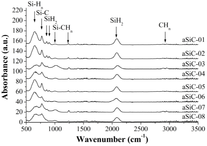
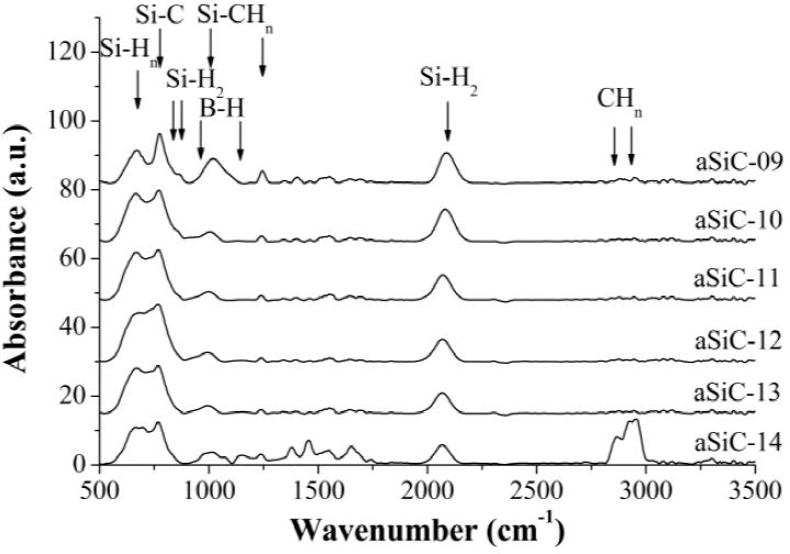
The FTIR spectrum of the film corresponding to the aSiC-14 process in Figure 2 includes two peaks at 975 and 1150 cm-1, which are assigned to the wagging and bending vibration modes of B-H bonds, respectively [14]. In the other spectra of the B-doped films only one shoulder at the left of the peak at 1000 cm-1 is observed, while no peak at 1150 cm-1 is displayed. The peaks in the band 2350 -2650 cm-1 corresponding to B-Hn bonds do not appear [15].
Optical characterization
The UV-visible spectroscopy was carried out in a spectrophotometer Perkin Elmer Lambda 3 from 190 to 900 nm, in order to obtain some optical properties of the films and correlate them with deposition parameters. Using the transmittance spectra and the Tauc equation given by [16]:
where h is the Planck's constant and v is the radiation frequency, the optical band gap (E gopt ) and the Tauc parameter (B factor) were found. B factor is a parameter that indicates the amount of disorder in a film [17].
The data fitting procedure using (1) resulted in the values summarized in Table 3. E gopt decreases around of 0.16 eV and 0.24 eV for XCH4 of 0.7 and 0.85, respectively, when ZH2 changes from 2.7 to 9.0. In undoped films, a trend is observed in B factor versus temperature under the same other deposition parameters, its value is higher at 200 °C than at 150 °C in the majority of cases. Regarding other deposition parameters (XCH4, ZH2 and power density), according to the results, their effect on B factor depends of the state of the remaining parameters. In B-doped films, the doping level decreases both E gopt and B factor.
Table 3 Optical band gap (E
gopt
), Tauc parameter (B),
activation energies (
| PECVD process |
Z H2 |
T (°C) |
E
gopt
(eV) |
B (eV cm) -1/2 |
(eV) |
(S/cm) |
(S/cm) |
|---|---|---|---|---|---|---|---|
| Undoped a-SixC1-x:H films: XCH4 = 0.7, 50 mW/cm2 | |||||||
| aSiC-01 | 2.7 | 150 | 2.05 | 497.75 | 0.73 | 954.90 | 1.05 × 10⁻⁹ |
| aSiC-02 | 9.0 | 150 | 1.90 | 489.34 | 0.73 | 1225.10 | 1.47 × 10⁻⁹ |
| aSiC-05 | 2.7 | 200 | 2.01 | 514.58 | 0.67 | 205.35 | 3.98 × 10⁻⁹ |
| aSiC-06 | 9.0 | 200 | 1.84 | 498.28 | 0.73 | 1166.05 | 1.08 × 10⁻⁹ |
| Undoped a-SixC1-x:H films: XCH4 = 0.85, 50 mW/cm2 | |||||||
| aSiC-03 | 2.7 | 150 | 2.47 | 426.24 | 0.70 | 369.57 | 5.55 × 10⁻¹⁰ |
| aSiC-04 | 9.0 | 150 | 2.23 | 523.64 | 0.74 | 2024.49 | 9.57 × 10⁻¹⁰ |
| aSiC-07 | 2.7 | 200 | 2.43 | 466.99 | 0.73 | 975.36 | 6.71 × 10⁻¹⁰ |
| aSiC-08 | 9.0 | 200 | 2.19 | 513.39 | 0.75 | 3757.39 | 1.17 × 10⁻⁹ |
| Undoped a-SixC1-x:H films: XCH4 = 0.85, 25 mW/cm2 | |||||||
| aSiC-09 | 2.7 | 200 | 2.42 | 534.74 | -- | -- | -- |
| aSiC-10 | 9.0 | 200 | 2.17 | 491.02 | 0.71 | 573.36 | 1.02 × 10⁻⁹ |
|
| |||||||
|
PECVD
process |
Yb
(%) |
E
gopt
(eV) |
B
(eV cm) -1/2 |
(eV) |
(S/cm) |
(S/cm) |
|
| B-doped a-SixC1-x:H films: XCH4 = 0.85, ZH2=9.0, 25 mW/cm2, 200oC | |||||||
| aSiC-11 | 0.5 | 1.96 | 449.68 | 0.41 | 0.81 | 1.72 × 10⁻⁷ | |
| aSiC-12 | 1.0 | 1.81 | 385.99 | 0.35 | 0.29 | 3.95 × 10⁻⁷ | |
| aSiC-13 | 2.0 | 1.80 | 395.70 | 0.33 | 0.73 | 2.72 × 10⁻⁶ | |
| aSiC-14 | 2.5 | 1.77 | 379.61 | 0.33 | 0.35 | 1.26 × 10⁻⁶ | |
Electrical characterization
Electrical dark conductivity measurements were carried out in the range of 300 - 440 K with a step of 10 K within the chamber of a Janis Research cryostat maintaining a pressure of 70 mTorr. Current-voltage measurements were made by using a Keithley 6517A and a LakeShore 331 temperature controller. Before measurements, the structures of undoped and B-doped a-SixC1-x:H/titanium on glass were annealed at 140 °C in nitrogen atmosphere for 2 hours to improve the contact between the material and titanium. In the Figure 3 can be seen that the curves are shifted upward by the change in hydrogen dilution from 2.7 to 9.0. This effect is more apparent in the films deposited at XCH4 = 0.85 than XCH4 = 0.70. In contrast, the B-doping not only shifts upward the curve but also changes its slope.
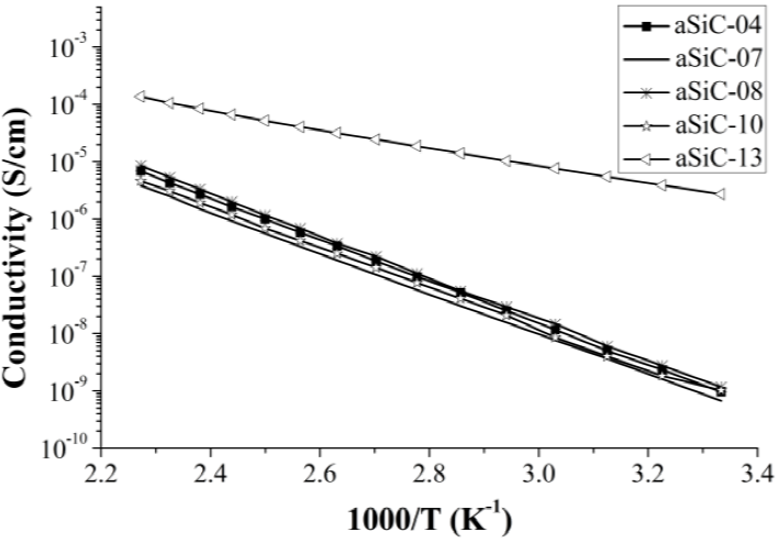
The values of conductivity for undoped and B-doped films calculated using the current-voltage measurements fall on one straight line; this straight line represents a thermally activated conduction regime and can be described by the following equation [18]:
where
Discussion
a-SixC1-x:H as material for interaction with biological media is one of the applications in which this material is suitable [1,2]. Its success in this applications (e.g. implants and implantable devices) is related with its density of Si-C bonds, its density of states (DOS) inside the band gap and its conductivity [8,19]. NSIC enhances the biocompatibility, inasmuch as Si-C bond (301 kJ/mol) is stronger than Si-Si bond (226 kJ/mol) [20], which results in greater chemical stability and low dissolution [6].
The Figure 2 shows that the peak at 780 cm-1 is affected by both XCH4 and ZH2. Increasing XCH4 from 0.70 to 0.85, NSiC increases and NSiH decreases because there are more methane molecules per radical silane; increasing ZH2 from 2.7 to 9.0, NSiC and NSiH increase. Hydrogen completes the dangling bonds in the amorphous structure, reducing the DOS within the band gap and improving the conductivity [21]. But in this case, under low power density of deposition, that is not the only effect. Considering the disappearance of the peaks in the band 2800-3000 cm-1 of the absorption spectra when hydrogen dilution is increased, hydrogen removes methyl groups, promoting the formation of Si-C and Si-H bonds and avoiding soft graphite-like structure.
Different trend is observed with doping. The Figure 4 shows that the peaks close to 770 cm-1 and 2080 cm-1 are reduced as the B-doping level increases (except the spectrum of the film corresponding to the aSiC-12 process), which means that B-doping decreases NSiC and NSiH (see also Table 1). In this case, the absorption by CHn groups increases as the doping level increases, achieving in the sample doped at 2.5% similar levels of absorption to those of Si-C bonds. This shows that as the doping level increases, the deposition control by reaction of methane and diborane molecules with silicon radicals is lower (dynamics of deposition). It increases both disorder within the amorphous structure and the surface roughness of the films. Furthermore, the peak at 2080 cm-1 shifts to 2060 cm-1 as the doping level increases. It is probable that this is due to lower concentration of carbon atoms and to the presence of boron atoms.
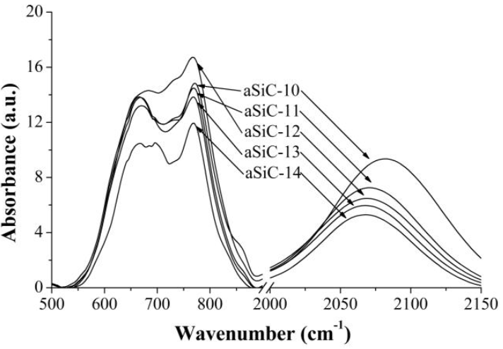
Figure 4 FTIR spectra in the ranges 500-900 cm-1 and 2000-2150 cm-1 of undoped and B-doped a-SixC1-x:H films.
Returning to the results of the optical and electrical characterizations, the ranges
of E
gopt
, B factor,
Applications as biosensors require a process known as bio-functionalization. This process is easier to achieve in smooth surfaces than in rough surfaces [22]. This work, consequently with other study [19], found that the deposition parameter that most affect the surface morphology is the power density. Films deposited at 25 mW/cm2 have root-mean square roughness less than or equal to 1 nm, even in B-doped films, where the incorporation of boron increases the disorder and the surface roughness. Again, these results are explained from the dynamics of deposition.
Other type of applications as neural interface devices [2], unlike these mentioned before, require a biocompatible material to encapsulate the device. In this case the deposition temperature must be lower than 200 °C and the conductivity must be as low as possible. Taking into account the requirements, the aSiC-03 process is the most optioned to fulfill this task. This process is carried out at 150 °C and a conductivity of 5.55 × 10⁻¹⁰ S/cm at room temperature was achieved in the corresponding film.
Summary and conclusions
By means of this study, the effects of hydrogen dilution and B-doping on the surface morphology and the structural, optical and electrical properties of a-SixC1-x:H films obtained by PECVD have been assessed under low power density, high pressure and low temperature deposition. The combination of high pressure and low power density allows to obtain root-mean square roughness in the sub-nanometric scale even in B-doped films, which is important when a bio-functionalization process is required to use the material. According to the results, hydrogen and diborane molecules compete with methane molecules and silane radicals to incorporate into the film by reaction with other silane radicals. Consequently, the methane-silane gas flow ratio must be kept high to prevent that the density of Si-C bonds is decreased and with it the biocompatibility of the material is impaired as well. The hydrogen dilution and B-dopind level must be low whether high optical band gap and low conductivity are required. In contrast, high hydrogen dilution, high B-doping level and high methane-silane gas flow ratio must be set to achieve high Si-C bond density, low DOS inside band gap and high conductivity regardless of the low optical band gap and the broader band tails.

