


 nova página do texto(beta)
 Inglês (pdf)
 Artigo em XML
 Referências do artigo
 Enviar este artigo por email
 Citado por SciELO
  Similares em
SciELO
Similares em
SciELO 
 Permalink
1. Introduction
ZnO is an inorganic transparent n-type direct bang gap metal oxide semiconductor with band gap energy of 3.36 eV at room temperature [1]. ZnO is used in diverse applications such as transparent electrodes in optoelectronic devices [2], heat mirrors [3], surfaces acoustic wave devices [4], and solar cells [5, 6]. In solar cells, the ZnO layer could be used as window layer, transparent conducting oxide and buffer layer. Several methods can be used to prepare ZnO thin films, such as pulsed laser deposition [7], chemical vapor deposition [8], sol-gel [5], molecular beam epitaxy [9] and reactive magnetron sputtering [10]. Among these methods, the magnetron sputtering method allows an easy control of the films structure and composition; additionally providing many advantages in reproducibility, high mechanical durability, strong adhesion and uniformity, as well as applicability to large area deposition.
On the other hand, thin film CdTe/CdS solar cells are typically on the configuration TCO/CdS/CdTe. The thickness of the CdS film is related to the number of incident photons that reach the CdTe. Therefore the decrease of the thickness of CdS increase the number of incident photons in the CdTe layer. However, as the thickness of CdS layer is decreased, localized CdTe/ transparent conductive oxide (TCO) junction are formed, which lead to excessive shunting and therefore lower the solar cell efficiency. Using high resistive transparent (HRT) layer is a feasible method to improve the characteristics of CdTe thin films solar cell. The ZnO is a promising candidate to be used as HRT layer in CdTe thin film solar cells. It is widely reported that inclusion of so-called HRT layer between TCO and CdS acts to enhance efficiency, although there is no consensus on the mechanism by which it occurs.
ZnO is also used as buffer layer in inverted organic solar cells [11] and polymer solar cell [12], improving its efficiency. On the other hand, Derkaoui et al. [13] reported the optical characteristics of multilayer coatings ZnO/CdS/CdTe using first-principles calculations, their results showed that the transmittance of the ZnO films had a sharp fall near the fundamental absorption, as the thickness increase; Liu et al. [14] reported an interface study of ITO/ZnO and ITO/CdS finding that the band offset of the ITO/ZnO and ITO/CdS were 0.4 eV and 0.9 eV, respectively. The thickness of the ZnO buffer layer in the solar cells is generally 100 nm, but in some cases, it could be used up to 500 nm. To the best of our knowledge, this is the first study of the minimal thickness of the ZnO layer in order to restrict the diffusion of ITO into the to CdS layer. In the present work we grew ZnO layers on ITO coated glass substrate. We studied the effect of the annealing on the ITO diffusion into the ZnO layer. The ITO/ZnO bilayer was characterized by X ray diffraction, UV-Vis spectroscopy and XPS. In order to study the effect of ZnO thickness on the efficiency of CdS/CdTe solar cells, we used an AMPS- 1D solar cell simulator.
2. Experimental procedures
ZnO thin films were grown by the reactive RF magnetron sputtering technique from a Zn metal target in an Ar-O2 gas mixture. Deposition was made onto ITO coated glass substrates (size 1" x 1") at a base pressure of 5x10 -6 Torr or better. The RF power applied to the target was set to 80W and the working pressure was 25 mTorr. The distance between the substrate holder and the target was 80 mm. The thickness of the film was monitored by a quartz microbalance in order to obtain samples with thickness of 100 nm, 200 nm, 300 nm and 400 nm. The substrate temperature was fixed at 400 °C. The oxygen and argon mass flows were fixed at 20 sccm and 5sccm, respectively. In order to promote the ITO diffusion into ZnO layer, in a similar manner that occurs during the CdS/CdTe solar cells construction, the bilayers of ITO/ZnO were thermally annealed at 540 °C by 1 hour. The identification code of the samples can be seen in Table 1. X ray diffraction (XRD) experiments were carried out in a Siemens D-5000 diffractometer using the Cu Kα radiation (λ=1.5406 Å). A Shimadzu UV-Vis spectrophotometer was used for collecting transmittance spectra of the films in the spectral range of 320-1000 nm. In order to obtain the diffusion of ITO into the ZnO layer, depth profile of the bilayer was characterized by means of X-ray Photoelectron Spectroscopy (XPS) (model K alpha by Thermo Scientific) for selected sample with ZnO thickness of 100 nm. The high resolution spectra in the regions of the C 1s, Zn 2p3/2, In 3d5/2, Sn 3d5/2 and O 1s were obtained after etching with Ar ions. The binding energy of the C 1s line at 284.5 eV was taken as the reference peak to calibrate the obtained spectra. The O 1s peak was fitted by employing asymmetric Gaussian-Lorentzian functions. The background subtraction was performed using the mathematical model derived by Shirley [15].

3. Results and discussion
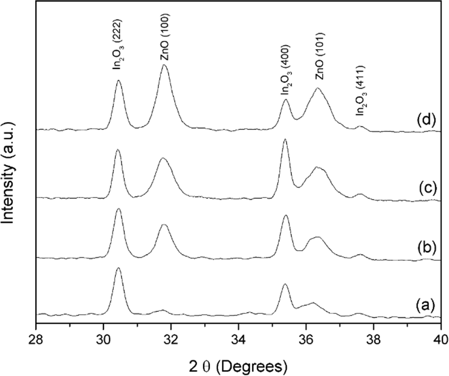
Figure 1 shows the XRD patterns of the ZnO thin films with a thickness of (a) 100 nm, (b) 200 nm, (c) 300 nm and (d) 400 nm; these were normalized with respect to the peak of the plane (222) of the In2O3. The diffraction peaks were indexed by using the cards No. 361451 and No. 060416 of Joint Committee of Powder Diffraction File database (PDF) for the ZnO and In2O3, respectively. The XRD patterns show that when the thickness of the film increase, the intensity of the peaks related to ZnO planes also increase.
The transmittance spectra of the ZnO films prepared with different thickness are shown in Figure 2; it can be seen a dependence of the transmittance with the thickness for wavelengths below the bandgap of the ZnO; it decreases with the raise of thickness. For wavelengths in the range of visible and near infrared spectrum, the transmittance for the samples grown at 400 °C and thermal annealed at 560 °C, had similar values.

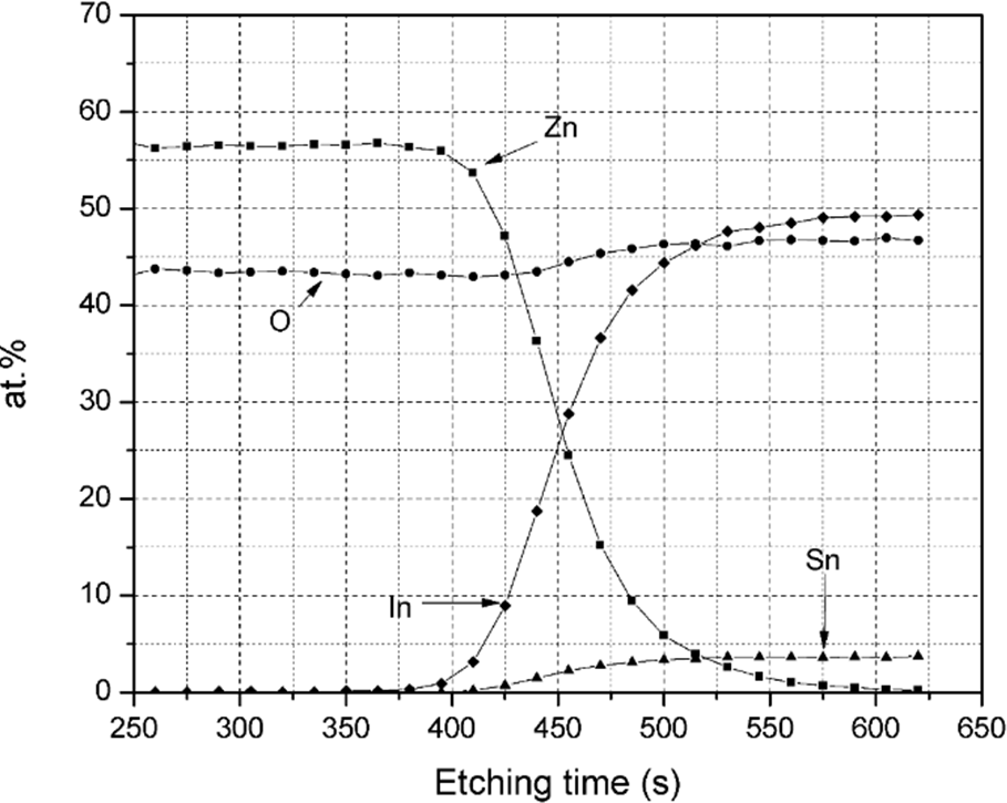
In order to determinate the minimal thickness of the ZnO as a buffer layer, depth profile concentration was realized in the sample with a 100 nm of thickness and thermal annealed. Figure 3 presents the concentration of Zn,O, In and Sn with respect the etching time. Before 350 seconds, only signals of Zn and O elements are observed, between 350 seconds and 575 seconds it can be seen the coexistence of Zn, O In and Sn elements; this result suggest the existence of ZnO and ITO composite. After 575 seconds only the elements corresponding to ITO are present. In a rough approximation, it could be assumed that the erosion is the same in all the thickness of the ZnO/ITO structure, as the thickness of the ZnO layer was 100 nm and the erosion time for this layer was 380 s and the erosion time for the ITO-ZnO composite was 180 s, the diffusion of the ITO into ZnO layer was estimated on the order of 50 nm; then this value is the minimum for the thickness of the ZnO without short circuits in the solar cell.
The XPS high resolution spectra for the Zn 2p3/2, In 3d5/2, Sn 3d5/2, showed that the binding energy associated with each element remains constant for all thickness. In figure 4 (a), the XPS high resolution spectra for O 1s is presented, the arrow direction indicates the increase of the etching time (this is from the ZnO towards the ITO). It can be seen a displacement in the binding energy; which is due to the different environment or bonding for the oxygen atoms. As the binding energy of oxygen 1s core level depends of chemical environment, curve fitting of the O1s XPS signal can be used to detect the bonding of the oxygen with the Zn, Sn and In. The XPS data analysis was performed with the XPSPeak4.1 program [16]. The O1s XPS signals were fitted with mixed Lorentzian-Gaussian curves. For the fit, the peak positions were maintained fixed (with values taken from the XPS database of the National Institute of Standards and Technology [17]). Also, the full width at half maximum (FWHM) was fixed for all peaks used for fitting the spectra, and the adjustable parameter was the intensity of the peaks. The experimental XPS peaks corresponding to the O 1s core level emission from different etching time are presented in figure 4; also it can be seen the fitted curves after deconvolution of experimental data, corresponding to the bonding of the oxygen with Zn, Sn and In. Figure 4 (b) shows the spectra with 310 s of etching with Ar ion, we can see that the spectra consists only of ZnO, with no evidence for the presence of SnO2 and In2O3. In Figure 4 (c) it is shown the XPS spectra with 460 s of etching time, it can be seen the contributions of ZnO, SnO2 and In2O3, which indicates the interdiffusion of ITO layer into the ZnO layer by the effect of the energy used in the deposition and the thermal annealing at 560 °C. Figure 4 (d) show XPS spectra with 575 s of etching time, it can be seen only the contribution of oxygen associated to bonds with Sn and In, which indicates only the contribution of the phases related with ITO (In2O3 and SnO2).
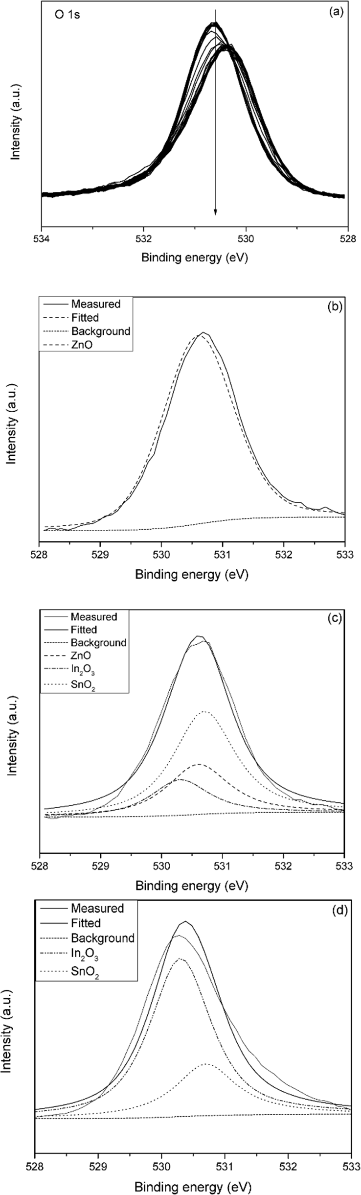
Figure 4. High resolution XPS spectra of O 1s at (a) for several ion Ar etching time (arrow indicates increase of the etching time),(b) etching time of 310 s, (c) etching time of 460 s and (d) etching time of 575 s.
AMPS 1D is a well-known solar cell simulation tool , it has been used in the simulation of different solar cells structures [18, 19]. The influence of ZnO thickness, on CdS/CdTe solar cells were studied by AMPS-1D simulation software. The parameters used in the simulation are shown in table 2; these were obtained from the reference 18. The values of the absorption index k, for each layer, were obtained for the figures reported by Treharne et al. [20]. In order to obtain the absorption coefficient α of the layers, the next equation was used:

where: k is the absorption coefficient and λ the wavelength.
For the calculation of the effect of the ZnO thickness layer on the CdTe solar cell characteristics, the ZnO thickness was changed from 0 nm to 700 nm, and the CdS thickness was kept fixed at 100 nm. The 0 nm value for the ZnO thickness indicates that we did not have the ZnO layer. As shown in Figure 5, the inclusion of the ZnO buffer layer increase the performance of the solar cell, these results may be due to an increase on the built-in electric field intensity [19]. The increase of the ZnO thickness decreases the efficiency, fill factor, Jsc and Voc slightly; these results could be due to the fact that when the thickness of ZnO layer was increased until 300 nm, the photons with energy below the bang gap energy of ZnO were totally absorbed and did not reach the CdS layer and in consequence the CdTe layer.

4. Conclusion
ZnO thin films were prepared by RF magnetron reactive sputtering on glass substrates coated with ITO. For a ZnO thickness of 100 nm and 200 nm, a portion of photons are not absorbed by this layer, hence they contributes to the efficiency of the solar cell. The interdiffusion thickness of the ITO into ZnO was around of 50 nm.

