


 nueva página del texto (beta)
 Inglés (pdf)
 Artículo en XML
 Referencias del artículo
 Enviar artículo por email
 Citado por SciELO
  Similares en
SciELO
Similares en
SciELO 
 Permalink
1. Introduction
Transparent conducting oxide thin films have important applications in the opto-electronics field as transparent electrodes [1], liquid crystal displays, IR detectors, thin film solar cells [2], etc. Cadmium oxide is an n-type semiconductor with a high mobility at room temperature (~ 216 cm2V-1s-1) and a bandgap value calculated in 2.18 eV [3], properties that make this material ideal for solar cells applications. CdO films can be prepared by different techniques, such as sputtering, metal organic chemical vapor deposition, ion beam sputtering, sol-gel, spray pyrolysis, chemical bath deposition (CBD) among others. For synthesizing CdO films by CBD, first CdO2 or Cd(OH)2 films are obtained and subsequently are subjected to a heat treatment [2,4]. In this work, we report on the influence of the cadmium nominal concentration in the CdO2 formation by CBD, and the formation of CdO by annealing in air.
2. Experimental details
2.1 Films growth
The CdO2 films were deposited on glass substrates by CBD at a bath temperature of 50 °C for 1 h. Before growth, substrates were cleaned in ultrasonic bath for 5 min by rinsing in successive steps in xylenes, ethanol, acetone and distilled water. The reaction solution was prepared mixing 40 ml of CdCl2, 20 ml of ammonium hydroxide (NH4OH) and 2 ml of H2O2. CdO2 films were deposited varying the CdCl2 concentration in: 0.030 M, 0.035 M and 0.040 M. DI water (18 MΩ) was used for the preparation of the solutions. The pH of bath was 11.5. After deposition, the films were rinsed in distilled water in ultrasonic bath and dried with nitrogen. Then, the as-grown films were heated at 300 °C in air by 1 h. As-grown CdO2 films were labeled from low to high CdCl2 concentration as: CD-01, CD-02 and CD-03 (see Table 1) whereas after the heat treatment samples were labeled CD-01-HT, CD-02-HT and CD-03-HT, respectively, (see Table 2).
Table 1 Physical properties of as-grown CdO2 films.
| Sample | [CdCl2] | Thickness | Eg |
|---|---|---|---|
| (M) | (nm) | (eV) | |
| CD-01 | 0.030 | 136 | 3.98 |
| CD-02 | 0.035 | 386 | 3.95 |
| CD-03 | 0.040 | 573 | 3.82 |
2.2 Characterization
X-ray diffraction (XRD) patterns were obtained in a Rigaku Smartlab diffractometer, using the Cu-Kα line (1.5406 Å). Electron diffraction patterns from selected areas were obtained by transmission electron microscopy (TEM) using a JEOL JEM 2010 microscope operating at 200 kV. Film thicknesses were measured in a KLA Tencor P15 profilometer. The topography studies were performed by Atomic Force Microscopy (AFM), using a ThermoMicroscope Autoprobe CP (Veeco Instruments) in contact mode. A Perkin-Elmer Lambda 25 UV-Vis spectrophotometer was used to obtain optical transmittance. Atomic concentration measurements of films were determined by Energy Dispersive Spectrometry (EDS) with a Bruker 5010 XFlash detector installed in a Jeol JSM-6300 scanning electron microscope.
3. Results and discussion
3.1 Structural characterization
XRD patterns of as-grown films are shown in Fig. 1a) . The CD-01 and CD-02 samples have two diffraction peaks of low intensity at 28.46° and 33.32°. The CD-03 sample presents four diffraction peaks at 28.46°, 33.32°, 47.66° and 56.76°. These peaks correspond to the cubic CdO2 (cadmium peroxide) phase and the diffraction planes are (111), (200), (220) and (311), respectively. The peaks were indexed using the powder diffraction files 39-1221 (PDF#39-1221). From Fig. 1a) it is noted that the crystalline quality improves as the CdCl2 concentration increases in the bath, indicating that the increase of the CdCl2 concentration promotes the formation of the CdO2 compound.

Figure 1 XRD patterns of a) CdO2 films grown by CBD and b) CdO thin films, produced after annealing the CdO2 films.
Fig. 1b) shows the XRD patterns of films after the heat treatment at 300 °C in air. Five diffraction peaks at 32.98°, 38.34°, 55.32°, 66.06° and 69.22° are distinguished, whose diffraction planes are (111), (200), (220), (311) and (222), respectively. These diffraction planes correspond to the cubic CdO. The peaks were indexed using the PDF#01-1049. It is important to mention that during the annealing, the CD-01 sample was totally evaporated. This indicates that an important amount of material evaporates during the annealing. Fig. 2 shows the transmission electron diffraction patterns of CD-03 sample before and after annealing. The electron beam incides into the [011] zone axis. The diffraction planes are indicated in Fig. 2. The electron diffraction patterns confirm that the CD-03 and CD-03-HT samples have a cubic structure; in fact, these samples have an fcc crystalline structure.

Figure 2 Diffraction patterns of a film deposited with a 0.040M CdCl2 concentration; a) CdO2 as-grown sample and b) after annealing.
As mentioned before, heat treatment desorbs the films surface. In order to know the evaporation rates, thickness measurements were performed. Table 1 shows the thickness of as-grown CdO2 films. The film thickness increases with the CdCl2 concentration, suggesting that the increase of the Cd nominal concentration promotes the formation of material, in agreement with XRD analysis in Fig. 1a) . Table 2 displays the thickness of the samples. The CD-01 sample was evaporated during the annealing so that the thickness of the CD-01-HT film was zero. Note from Table 1 and Table 2 that during the heat treatment a great amount of material evaporates. The thicknesses evaporated (summarized in Table 2), from CD-01, CD-02 and CD-03 were 136 nm, 256 nm and 282 nm, respectively.
Due to the high amount of material evaporated, the topography of samples after heat treatment must change drastically. In order to know the topography of the films AFM measurements were carried out. The surface morphology of films is shown in Fig. 3. AFM images corresponding to the as-grown CdO2 films are displayed in the left column, whereas those of CdO films (annealed films) are placed in the right column. The surface of the CD-01 sample (Fig.3 a) shows holes, which indicates that for a 0.030 M CdCl2 concentration the formation of the CdO2 film begins. The surface morphology of CD-02 sample is shown in Fig. 3b) . This sample has large clusters of around 500 nm. Comparing images CD-02 and CD-HT-02 (Figs. 3b and 3d ) there is no significant difference between the two surfaces. However, differences between the surfaces of the CD-03 and CD-HT-03 samples are notable. Fig. 3c) displays the surface of the CD-03 sample, showing grains of irregular shape, distributed in a periodic array. These grains decrease in dimensions after heating the sample as corroborated in Fig. 3e) . The optical properties of the CdO samples are strongly related to the size of these grains. In the following paragraphs, we will further discuss this idea.
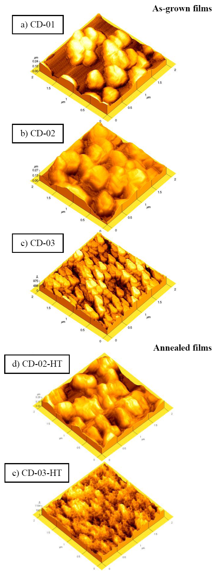
Fig. 4a) shows the transmittance spectra of as-grown CdO2 films. The CD-01 and CD-02 samples present absorption of light in the wavelength region ≥ 400 nm, which can be attributed to crystalline defects, that are responsible of the reduction of transmittance [5]. The CD-03 sample has a high transmittance in the visible region (>70%) and the spectrum presents an absorption edge practically vertical, indicating a good crystalline quality of the sample (in agreement with the XRD results). The transmittance spectra of films with heat treatment are shown in Fig. 4b) . Note that the heat treatment reduces the transmittance of films and shifts the absorption edge towards the yellow. From these spectra the absorption coefficient (α) was calculated by the relation: T=(1-R)2exp(-αd), where T is the transmittance, R the reflectance and d the film thickness [5]. The absorption coefficient was used to determine the bandgap (Eg ) of films, using the relation αhν = (hν-Eg )1/2, where hν is the photon energy [1,5].Fig 5 shows the graphic of (αhν)2 vs hν, the Eg was determined by fitting the lineal part of the curve. The bandgap values of the as-grown CdO2 films are compiled in Table 1, the bandgap value decreases from 3.98 eV to 3.82 eV as the CdCl2 concentration in the bath increases. The Eg value calculated for CdO films; CD-02-HT and CD-03-HT, was 2.38 eV and 2.59 eV (see Table 2), respectively, in agreement with the bandgap values reported in the literature [6]. Pan et al [7]. reported that the grain size decrease in CdO samples produces an increase in their bandgap. Encompassing the same consideration the AFM images of Figs. 3d) and 3e) show that CdO surface grains decrease from sample CD-02-HT to CD-03-HT. We infer that the grain decrease observed by AFM is responsible of the bandgap widening in our samples synthesized with the highest concentration of CdCl2, suggesting that the molar concentration has strong influence in the grain size. This result will be subject of another publication concerning electrical properties of the samples. The increase in the bandgap has been explained in terms of the Burstein-Moss effect as long as the intrinsic physical properties of CdO samples [7,8].
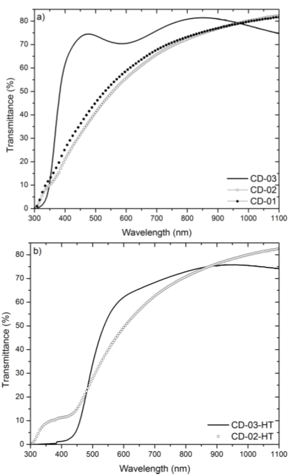
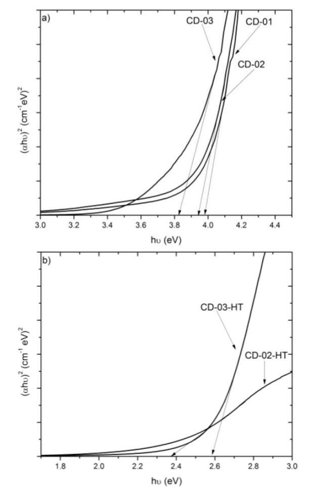
Fig. 6a) and Fig. 6b) show the EDS spectra of CD-03 and CD-03-HT samples, respectively. Peaks associated to cadmium (Cd), oxygen (O), sodium (Na), magnesium (Mg), silicon (Si) and calcium (Ca) are indicated. In Fig. 6a) peaks corresponding to Ca, Si, Mg and Na are of low intensity, while those associated to Cd and O are of high intensity. Peaks of low intensity are due to substrate, whereas detected peaks of Cd and O correspond to the CdO2 compound formation. The oxygen peak is about three times more intense than that corresponding to cadmium; this is because a fraction of the oxygen detected corresponds to the substrate. Fig. 6b) shows the spectrum of CD-03-HT. After annealing the intensity of peaks corresponding to the substrate increases, due to the reduction of film thickness by evaporation. In spite the intensity of cadmium and oxygen peaks decreases after annealing, Fig. 6b) shows Cd and O signals are similar in intensity, suggesting the CdO compound formation.

4. Conclusions
Cadmium peroxide (CdO2) films were obtained by CBD using CdCl2 as cadmium source. The physical properties were analyzed as a function of CdCl2 concentration. X-ray diffraction showed that CdO2 films have the cubic stable phase. The structural, morphological and compositional characterization showed that the increase of the CdCl2 concentration promotes the formation of CdO2 compound. For a 0.040 M CdCl2 concentration CdO2 films with a high crystalline quality were obtained. CdO2 films were annealed in air at 300 °C for obtaining CdO films. The structural characterization of the annealed films showed that CdO samples have cubic structure. Bandgap values of 2.38 and 2.59 eV were estimated from optical characterization. This widening in the bandgap was explained in terms of the Burstein-Moss effect.

