


Servicios Personalizados
Revista
Articulo
 Inglés (pdf)
 Artículo en XML
 Referencias del artículo
 Enviar artículo por email
Indicadores
-
 Citado por SciELO
 -
 Accesos
Links relacionados
-
 Similares en
SciELO
Similares en
SciELO
Compartir

 Permalink
Superficies y vacío
versión impresa ISSN 1665-3521
Superf. vacío vol.27 no.3 Ciudad de México sep. 2014
Polycristalline growth of zinc blende gallium arsenide layers by R.F. magnetron sputtering
Bernal Correa R.1,2* , Montes Monsalve J.1,2, Pulzara Mora A.2**, López López M.3, Cruz Orea A.3 y Cardona J.A.4
1 Escuela de Materiales, Universidad Nacional de Colombia, sede Medellín, Colombia. * rabernalco@unal.edu.co, ** aopulzaram@unal.edu.co
2 Laboratorio de Nanoestructuras Semiconductoras, Grupo Magnetismo y Materiales Avanzados, Universidad Nacional de Colombia, sede Manizales. A.A. 127, Colombia.
3 Departamento de Física, Centro de Investigación y de Estudios Avanzados del l.P.N Apartado Postal 14-740, 07000, México D.F, México.
4 Grupo de Investigación en Materiales Semiconductores y Superiónicos. Departamento de Física Facultad de Ciencias. Universidad del Tolima. Alto de Santa Helena. Ibagué. Colombia.
Recibido: 21 de abril de 2014;
Aceptado: 01 de septiembre de 2014
Abstract
Zinc-blende GaAs layers were prepared on (100) Si and glass substrates by r.f. magnetron sputtering. The morphology of GaAs layers is analyzed by means of atomic force microscopy (AFM) and scanning electron microscopy (FE-SEM), to determine the sample topography and growth type. The compositional analysis was performed by means of energy dispersive X-ray spectroscopy (EDS), in order to obtain information of the atomic percentages of the elements and their spatial distribution in the samples. The optical properties of the layers are discussed from the results of UV-Vis absorption, and Photoacoustic spectroscopy (PAS). Finally, the Raman shift of the GaAs phonon modes are studied as function of the penetration depth of laser wavelength used to excite the sample on Raman microscopy.
Keywords: Gallium arsenide, RF magnetron sputtering, Raman microscopy.
1. Introduction
In spite of the fact that gallium arsenide (GaAs) is the most widely studied III-V semiconductor [1,2], remains topical issue, due to that the research are focusing on the search of new preparation methods at lower cost. In recent years there has been a strong interest in obtaining gallium arsenide on transparent substrates, e.g. corning glass [3,4], important for the development of photovoltaic technology. On the other hand, growth of GaAs onto Si substrate offers very attractive potential to incorporate future GaAs devices onto silicon-based very large scale integrated circuits. Due to the large difference in lattice constants (αGαAs = 5.653 Å, αsi = 5.431 Å, and Δα = -4.09%) between the GaAs layer and Si substrate, it is not easy to epitaxially grow GaAs on Si and amorphous glass substrates, including methods such as pulsed laser deposition (PLD), chemical beam epitaxy (CBE) and molecular beam epitaxy (MBE) [5-7]. The growth of GaAs on Si (100) substrates by magnetron sputtering (MS) in most cases result in an amorphous structure [8,9]. However, some reports indicate that an annealing at temperature of 260 °C, in an inert atmosphere changes the orientation of the samples along on (111) directions [10]. Besides, thermodynamic parameters such as temperature, pressure, working gas, etc. are also crucial in the crystalline quality of the samples.
In this work, we report the growth of polycrystalline zinc-blende gallium arsenide deposited on glass and (100) Si substrates by using r.f. magnetron sputtering. In order to study their optical, morphological and structural properties, we carried out experiments of XRD, Raman, SEM, AFM and absorption spectra in the UV-visible range.
2. Experimental
The gallium arsenide layers were deposited by RF magnetron sputtering in an Argon (Ar) atmosphere at a pressure of 5x10⁻³ Torr. The residual pressure in the chamber was of 1x10⁻⁶ Torr. The layers were deposited on Si (100) and glass substrates (labeled M1 and M2) previously treated in a bath of acetone in an ultrasound for 10 minutes. The r.f. power supply of the GaAs target and substrate temperature were maintained constants at 30 Watt and 580 °C for all samples, respectively. The layer thickness was obtained from SEM micrographs taking in cross sectional, and the crystal quality was determined by X-ray diffraction (XRD) at a rate of 1°/min with a step of 0.02°, in the range 20 ° ≤ 2θ ≤ 60 ° (XRD System-irradiation Rigaku Cu Kα = 1.5405 Å. Raman microscopy in backscattered configuration with direction perpendicular to the sample and unpolarized beam was used to study the behavior of TO and LO vibrational modes of the InGaAs layers (Raman Dilor XY Labram spectrometer equipped with an Olympus BX40 and three laser lines of 488 nm, 532 nm and 632 nm), the spectra were collected in the backscattering geometry and un-polarized beam. The morphology and composition were analyzed by scanning electron microscope FE-SEM on a JEOL JSM7401F equipment, and atomic force microscopy (AFM) was used to calculate the roughness values in an area of 2x2 μm2
The band gap energy values were obtained from results of PAS and UV-Vis, for samples Ml) and M2) respectively.
3. Results
The results obtained from X-ray diffraction revealed two possible phases in the GaAs layers deposited on Si and glass substrates, labeled as (M1) and (M2), respectively. The first one, deposited on (100) Si presented a ZB-type crystalline structure with a preferential orientation along of (111) direction, as show in Fig. 1.a).The peak's intensity is sharp and narrow, showing that the GaAs sample has a good crystalline quality, and fine grain size. The (002) plane located at 2θ = 32.5° is attributed at single crystal Si substrate, according to the diffractogram (M1-substrate) taken as reference. No extra diffraction peaks corresponding to GaAs phases are evidenced, indicating that the GaAs samples are crystalline. The (004) Si main plane located at 28 = 65°is out of the range and not shown here.
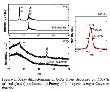
For gallium arsenide layer deposited on Si (100), is calculated the crystallite size from Scherrer's equation (1):
Where β is the line width at half maximum height, λ is a wavelength in nanometers of the x-ray radiation (Cu-Kα = 0.15406 nm), K is a constant related to crystallite shape, normally taken as 0.9, θ is the diffraction angle and D is the crystallite size [11]. From experimental values obtained from X-ray (β = 0.2841, θ = 13.61), showing in the (Fig. 1c), the nanocrystalline size was 28 nm. On the other hand, the sample deposited on glass substrate presents a polycrystalline structure, Fig. 1b). In these spectra, the planes located at 2θ = 27 ° and 45 ° corresponding to the (111) and (220) crystallographic directions come from cubic ZB structure of the gallium arsenide. In the X-ray difractograms, it is observed that the peaks are not well defined; they are noisier and weaker than previous one, due to the structural disorder or possibly to the clusters formation.
The difference in crystalline quality observed in our samples is mainly attributed to the substrate type involving lattice mismatch, and thermal coefficient. Another's factors affecting the orientation and crystalline quality are the alloying and stress effects, being the last one, the most influential factor to obtain good crystalline quality samples.
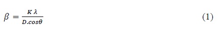
The layers were also evaluated compositionally and morphologically using scanning electron microscopy, and atomic force microscopy. Figures 2a) and 2b) show cross-sectional SEM images along the entire layer thickness deposited on Si (100) substrate at 10.000 X and 50.000X magnification, respectively. A clear interface was visible between layer and substrate (Figure 2a).The layer is uniform and relatively smooth in a large region, and it is not observed agglomeration effects or porosity. Columnar growth can be clearly observed in this layer (Figure 2b).
Energy dispersive X-ray analysis (EDS) carried out on surface (plan view) and cross-section along of all thickness of the layer, confirm that As/Ga ratio is nearly stoichiometric, as shown in Table 1. In order to correlate the microstructure and the distribution of Ga and As elemental map (5000X magnification) were recorded. The mapping images of Ga and As are shown in Figure 2-c) and 2-d). The corresponding Ga and As maps show a homogenous distribution of both Ga and As elements, in good agreement with EDS analysis.
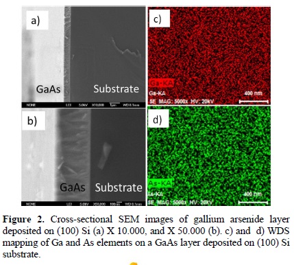
AFM images that were employed to analyze the surface topography of the layers and to measure their roughness, are shown in the Figure 3a) - 3b), for the samples deposited on Si (100) and glass. The AFM images do not show considerable differences on their topography. The roughness of the GaAs layers was estimated in a 2x2 μm2 area. The root mean square (RMS) roughness parameter (Rq) for the GaAs samples deposited on Si (100) and glass substrates were of 30 nm and 40 nm, respectively.
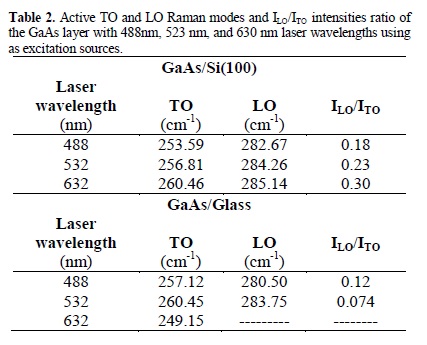
The vibrational modes were studied by means of Raman spectroscopy using three different laser wavelengths (λ1 = 488nm, λ2 = 532 nm and λ3 = 632 nm) as excitation sources. Because the zinc-blende structure belongs to cubic space group F-43m, in zinc-blende GaAs TO and LO modes are split at k = 0 due to its polar nature [12]. These results are consistent with those obtained from X-ray, where a polycrystalline formation is observed and only reflections (111) are present.
Figure 4-a) show the spectra of the layer GaAs deposited on Si (100) employing laser excitation wavelength of 488nm, 532 nm and 632 nm. In the spectrum of the GaAs/Si(100) layers obtained using 632 nm excitation line (Figure 4 below), it can be seen that peak position corresponds very well with the position of the TO (261 cm-1) and the LO (285 cm-1) modes measured on the bulk (111) GaAs. With 532 nm and 488 nm excitations (the middle and upper line in Figure 4), it is also observed the GaAs Raman modes, but they are presented a shift to lower energies. In all samples the (ITO/ILO) integrated intensity ratio is less than one, in good agreement with theoretical predictions, because the Raman signal comes from (111) reflection peak (table 2.). For laser excitation of 532 nm excitation, the intensity of the Raman modes is less than compare to the intensity of the modes seen 632 nm and 488 nm. One possible reason of this fact is the focus position used to obtain the spectrum.
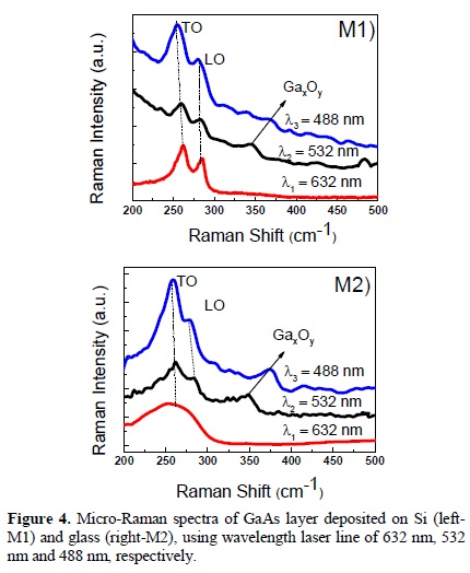
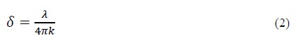
On the other hand, with wavelength lasers excitation of 532 nm and 488 nm several unusual satellites peaks of GaxOy were observed on background of the GaAs Raman spectra. In contrary, the Raman spectrum with wavelength laser excitation of 632 nm is flat and it is only observed the LO and TO GaAs-like phonon modes belonging to GaAs bulk. In order to analyze this point, we calculated the spatial extent over which the light is absorbed namely optical penetration depth or skin depth, which is define as:
where λ is the light wavelength used as excitation source, and k is the imaginary part of the complex ñ = n + ik refractive index. The values obtained by eq. (2) were δ = 81 nm, 132nm and 251.4 nm [13] for 488nm (2.54 eV), 532nm (2.33 eV) and 632 (1,9eV) nm excitation laser wavelengths, respectively. It can be see that Raman intensity of the satellite peaks excited with a wavelength of 488 nm (δ = 81 nm) are more intense than those excited with wavelength of 632 nm (δ = 251 nm). It is only possible if the incident laser energy is close to energy of the electronic transitions, effect known as resonant Raman (RR), raising the intensity of GaxOy Raman modes. The Raman bands at 198, 346, 416, 476, 654, and 776 cm-1 have been reported by Sulikowski et al [14] and and Zhang et al [15] in β-Ga203 bulk. The bands between 300- 600 cm-1 correspond to bending vibrations while those above 600 cm-1 are due to Ga-04 tetrahedral stretching. On the other hand, although the Ga203 emit in 4.9 eV, the PL blue signal at 2.9 has been reported, originated from recombination between an oxygen vacancy pair in the donor band and a gallium-oxygen vacancy pair in the acceptor [16].
The depth profile of oxygen concentration in the layers was checked by secondary ion mass spectroscopy SIMS (not shown in this paper). The SIMS spectrum shows a higher concentration of oxygen, on the surface, as a result of being exposed to the environment, and then it decreases in lesser proportion inwards of the sample until about 100 nm depth. Furthermore a significant increase in oxygen amount at the interface due to incomplete desorption of the oxide during degassing of the substrate made 580 ° C was observed. This suggests that the vibrational modes of GayOx in the Raman spectra obtained with laser lines 488, 532, and 632 nm not come from the same volume in the sample, and probably Ga-0 bonds at the surface and at the interface are different, in good agreements with the Raman shift observed in these spectra.
The shift observed in the TO and LO of the GaAs-like Raman modes, Figure 4-M1), is likely due to growth-strain induced during layer deposition by the lattice (Δa = 4%) and thermal mismatching of the substrate (silicon) and GaAs layer [17, 18]. The shift observed in these spectra is probably due to that GaAs layer tend to be amorphous at the beginning of growth, but it improves the crystalline quality at the end of it (see SEM images of the Fig. 2 a) and b)). The Raman shift by single crystal and polycrystalline materials have been reported in many materials [19].
On the other hand, in the GaAs layer deposited onto a glass substrate (Figure 4 b), the behavior of the TO and LO Raman modes associated to GaAs with 488 nm and 532 nm laser excitation lines, are very similar to those observed in GaAs layers deposited on Si (100), discussed in the previous section. However, a different behavior is observed with 632 nm (≈650 nm thickness layer) laser excitation line. In this case, the TO and LO Raman modes are very wider. It is showing that at the beginning of the growth the GaAs layer tend to be amorphous, because it replicates the structural disorder of the glass substrate, then the layer improves the crystalline quality until the end of growth, in good agreement with X-ray spectrum of the Figure 1.
To obtain optical energy band gap (Eg), we carried out photo-acoustic spectroscopy (PAS) measurements in the GaAs layer deposited on Si (100), sample Ml. The room temperature (RT) PA intensity spectrum as a function of excitation energy is shown in Figure 5. In this spectrum, it is observed that the photoacustic (PA) signal decreases with excitation energy increases, until reach its minimum (region I) just below of the GaAs absorption edge, due to the absorption silicon substrate. We used this criterion o determinate Eg (=1.43 eV) of GaAs layer. The minimum in the PA intensity is characteristic of a transition between nonradioactive bulk recombination processes to surface recombination process.
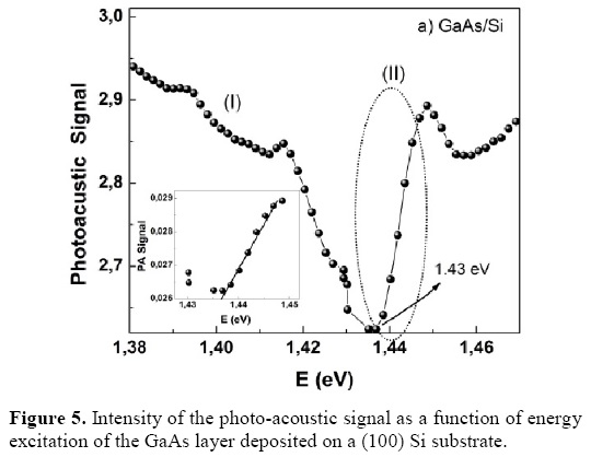
The absorption edge of the GaAs layer (region II) is indicated by a dot circle line, in Figure 5. The inset of this figure shows the best fit (region II) using the equation (3) of direct semiconductor band gap,
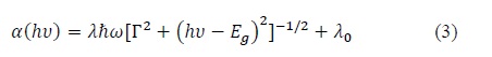
Where Γ is the damping parameter and λ0 is a constant added to correct the possible error on the origin of the data [20]. The value of band gap (Eg) obtained was of 1.435 eV in good agreement with reported value [21]. The peak observed just above of fundamental band gap problaly come from free excitons.
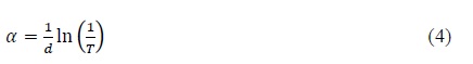
For the GaAs layer deposited on a glass substrate (sample M2), we performed transmittance measurements in the range of 300 to 1200 nm. From transmittance spectrum the absorption coeficient (α)is calculated using the Lambertt's law:
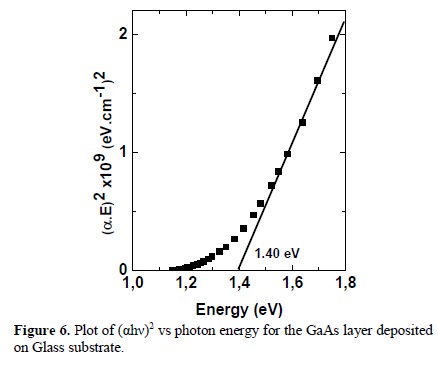
where T is the transmittance and d is the layer thickness (d = 650 nm obtained from SEM cross-sectional images). It is well known that the GaAs is a direct band gap semiconductor, thus the absorption coefficient (α) can be described as a function of the incident photon energy by the relation,
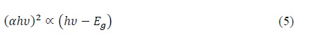
Where hv is the excitation energy, Eg is the band gap [18]. The band gap is obtained by extrapolating the linear part of curve to the zero of (αhv)2. Fig. 6 shows the (αhv)2vs hv plot of the GaAs layer. The band gap value of GaAs layer is found to be 1.40eV.The shift of the reported fundamental band gap (ΔEg= 0,03eV) to lower energies is attributed a possible deformation of the lattice due to the high density of crystal defects.
4. Conclusions
Gallium arsenide layers with columnar growth and preferential crystallographic orientation in direction (111) on Si substrates (100) were prepared by magnetron sputtering. The band gap of the GaAs layers obtained from photo-acoustic and absorbance are consistent with the reported values. The analysis of the vibration modes made as a function of penetration depth, show that the GaAs layer on glass substrates tend to be amorphous at the beginning of growth, but it improves the crystalline quality at the end of it. The result shows that magnetron sputtering is a good technique to prepare polycrystalline GaAs layers. Finally, photoacoustic spectroscopy is a technique useful for determining the bandgap energy of III-V semiconductor layers, e.g InGaAs deposited on non-transparent substrates.
Acknowledgments
Dirección de Investigaciones (DIMA) de la Universidad Nacional de Colombia sede Manizales. Solid State Physics, Physics Department, CINVESTAV-IPN México D.F. Roberto Bernal-Correa and Jorge Montes Monsalve, thank COLCIENCIAS for scholarship "Francisco José de Caldas" Convocatoria 520. A. Pulzara Mora thanks to Secretaría de Ciencia, Tecnología e Innovación de Distrito Federal (CECITI-DF) and Centro Latinoamericano de Física (CLAF) for financial support.
References
[1]. J. O. Akinlami, and A. O. Ashamu, Journal of Semiconductors 34, 32002 (2013). [ Links ]
[2]. M. M R Howlader, F. Zhang and M J. Deen Nano technology 24, 315301 (2013). [ Links ]
[3].Erlacher, M. Ambrico, V. Capozzi, V. Augelli, H. Jaeger, and B. Ullrich, Semicond. Sci. Technol. 19, 1322 (2004). [ Links ]
[4]. R.R. Campomanes , J.H. Dias da Silva , J. Vilcarromero , L.P. Cardoso, Journal of Non-Crystalline Solids 299, 788 (2002). [ Links ]
[5].M. Imaizumi, M. Adachi, Y. Fujii, Y. Hayashi, T. Soga, T. Jimbo, M. Umeno, Journal of Crystal Growth 221, 688 (2000) [ Links ]
[6]. S. Kalem, B. Jusserand, Appl. Play. A 62, 237 (1996) [ Links ]
[7].A. Erlacher, B. Ullrich, EY. Komarova, H. Jaeger, H.J. Haugan, G.J. Brown, Journal of Non-Crystalline Solids 352, 193 (2006) [ Links ]
[8]. Y. Yan-Ping, L. Chun-Ling, Q. Zhong-Liang, L. Mei, G. Xin, and B. Bao-Xue, Chin. Phys. Lett., 25, 1071 (2008). [ Links ]
[9].T. Z. A. Zulkifli, D. L. Rode, L. H. Ouyang, and B. A. Shrauner, Universiti Sains Malaysia http://csmantech.pairserver.eom/Digests/2004/2004Papers/8.3.pdf [ Links ]
[10]. R.R. Campomanes, J. Ugucion, J.H. Dias da Silva, Journal of Non-Crystalline Solids 304,259 (2002). [ Links ]
[11]. P. Scherrer, Gottinger Nachrichten 394 (1918) [ Links ]
[12]. P.Puech, G.Landa, Robert Carles, and C. Fontaine, J. Appl. Phys 82,4493 (1997) [ Links ]
[13]. Z. C. Feng, A. A. Allerman, P. A. Barnes, and S. Perkowitz, Appl. Phys. Lett. 60,1848 (1992). [ Links ]
[14]. B. Sulikowski, Z. Olejniczak, and V. C. Corberan, J. Phys. Chem., 100, 10323 (1996). [ Links ]
[15]. H. Z. Zhang, Y. C. Kong, Y.Z. Wang, X. Du, Z. G. Bai, J. J. Wang, D. P. Yu, Y. Ding, Q. L. Hangand, S. Q. Feng, Solid State Commun., 109, 677 (1999) [ Links ]
[16]. L. Binet, D. Courier. Phys. Chem. Solids, 59, 1241 (1998) [ [ Links ]17]. S C Jain, M Willander, and H Maes, Semicond. Sci. Technol. 11,641 (1996). [ Links ]
[18]. J. I. Pankov, Optical Processes in Semiconductors, Dover. 1,34 (1971). [ Links ]
[19]. J. Caetano de Souza, A. Ferreira da Silva and H. Vargas. Journal de Physique IV. Colloque C7, supplement au Journal de Physique II, Volume 4, 129 (1994). [ Links ]
[21]. J. S. Blakemore, J. Appl Phys 53, 123 (1982). [ Links ]

