


Servicios Personalizados
Revista
Articulo
 Inglés (pdf)
 Artículo en XML
 Referencias del artículo
 Enviar artículo por email
Indicadores
-
 Citado por SciELO
 -
 Accesos
Links relacionados
-
 Similares en
SciELO
Similares en
SciELO
Compartir

 Permalink
Superficies y vacío
versión impresa ISSN 1665-3521
Superf. vacío vol.27 no.1 Ciudad de México mar. 2014
Effects of temperature and deposition time on the RF- sputtered CdTe films preparation
Camacho-Espinosa E.*, Rosendo E.*, Díaz T.*, Oliva A. I.**, Rejon V., Peña J. L.**
* Centro de Investigación en Dispositivos Semiconductores, BUAP 14 Sur y Avenida San Claudio, C. U. Edificio 103-C, C.P. 72570 Puebla, Puebla México. *ed_cam_es@hotmail.com.
** Centro de Investigación y de Estudios Avanzados del IPN Unidad Mérida. Depto. Física Aplicada Km. 6 Antigua Carretera a Progreso, A.P. 73-Cordemex C.P. 97310 Mérida Yucatán México.
Recibido: 28 de octubre de 2013;
Aceptado: 22 de febrero de 2014.
Abstract
In this work, CdTe thin films were deposited by rf-sputtering at different substrate temperatures (room temperature (RT), 100, 150, 200, and 250 °C) and deposition times (30, 60, and 90 min). The applied power and vacuum pressure were maintained fixed for all depositions. A mean value of 18.5 nm/s on the deposition rate was maintained for films deposition. The surface morphology, rms-roughness, and grain size of the sputtered-films were obtained from atomic force microscopy and scanning electron microscopy images for comparison. CdTe films deposited during 60 min presented high reproducibility, because their consistent thickness value (1.2 μm) at different substrate temperatures. Higher thickness than 1.81 μm was obtained for films deposited at 250 °C and 90 min. CdTe films deposited at 150 °C present minor dispersion on thickness, while rms-roughness increased with the increase of substrate temperature but only for films deposited at 60 and 90 min. CdTe film deposited at 250 °C during 90 min was selected as appropriate for CdS/CdTe solar cells preparation.
Keywords: Magnetron sputtering; CdTe; Substrate temperature; Thin films.
1. Introduction
Cadmium telluride (CdTe) films are nowadays object of study, given its importance as absorbent layer in the CdS/CdTe solar cells. This type of solar cell is the second most important in the industrial production which represents 7 % of the total solar cells [1]. The principal advantage of this type of solar cells is the thinner thickness as compared with the crystalline silicon solar cells. This advantage permits easy manipulation, flexibility, and minor costs. Another important advantage of this kind of solar cell is its facility for fabrication as compared with other types of thin film solar cells such as CuInSe2 or amorphous Si:H. According to theoretical calculations, the CdS/CdTe solar cells can reach an efficiency of 29% [2]. Currently, an efficiency of 19.9% has been reported for CdS/ CdTe solar cells for laboratory conditions [3]. Thus, different efforts in this way are currently doing in order to increase the efficiency such that intensive study of each component is required. According to previous works, for CdS/CdTe solar cells, a CdTe thickness between 1.5 and 2 μm is highly desirable [4].
Changes in CdTe morphology by increasing the substrate temperature have been studied by different deposition techniques. For example, Rigana-Begam et. al. [5] studied the structural, morphological and optical properties of CdTe deposited by electron beam evaporation technique by varying the substrate temperature at 150, 300, 350 and 400°C.
However, there is not enough work done for CdTe films deposited by the sputtering technique, despite the known importance as a suitable technique for solar cells large scale-applications.
Substrate temperature plays an important role in the morphological CdTe films [6]. Despite the importance in the substrate temperature scarce work have done in try to determine the best substrate temperature for CdTe deposition by sputtering technique, in this work we contribute a little in this issue. Additional to this no reports have been found where the CdTe was deposited at relatively low temperatures (100 °C and 150 °C) with sputtering technique, where the grain size was reported, which is done in this work.
In this work CdTe thin films were deposited by magnetron sputtering technique under different temperature conditions, varying from room temperature (23°C) to 250 °C and for three specific deposition times 30, 60 and 90 minutes. Structural and morphological characteristic of films as a function of substrate temperature and deposition time were studied. It was estimated the deposition rate and thickness of the samples. The surface roughness of the CdTe films was measured from AFM images.
2. Experimental Procedure
Cadmium telluride (CdTe) thin films were deposited by sputtering technique onto glass substrates (1x1 in2). A commercial CdTe target of 99.999% purity and 1 inch in diameter was employed. For deposition, the base-pressure of the vacuum chamber was 2x10⁻⁵ Torr, and the substrate-target distance was 5 cm. The substrates are heated by Joule effect with a tungsten lamp of 150 W controlled by an autotransformer Variac, which regulates the energy delivered to the lamp. The deposition of films was made with a RF source Kurt J. Lesker model R 301, using a circular magnetron sputtering source from Kurt J. Lesker model 1HV TORUS. Pressure of argon gas was manually controlled by means of a needle valve. Thin films were deposited at different substrate temperatures: room temperature (RT), 100°C, 150 °C, 200 °C, and 250 °C. For each substrate temperature selected three different films with deposition time of 30, 60, and 90 min were deposited, while the rf-power was maintained at 40 W and the pressure at 10 mTorr. In order to estimate the deposition rate, a profilemeter Veeco model Dektak 8 was used to measure the film thickness. The surface morphology of the deposited CdTe films was discussed from 0.5 x 0.5 μm2 images obtained with a non-contact atomic force microscopy (AFM) Ambios Universal. The shape of grains and cross section of deposited films were also observed with a scanning electron microcopy (SEM) Jeol JSM-7600F.
3. Results and Discussion
3.1. Deposition rate and thickness
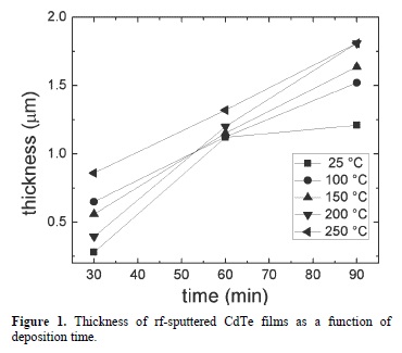
Figure 1 shows the thickness values of the CdTe films deposited as a function of the different substrate temperatures and deposition times. From Figure 1 can be appreciated the increment of film thickness with deposition time, obtaining values up to 1.8 μm for samples deposited for 90 min and 250 °C as substrate temperature. However, for CdTe films deposited at room temperature the increase in thickness with deposition time is less than the observed for CdTe films deposited at other substrate temperatures. On the other hand, it can be observed that the film thicknesses increase with the increment of substrate temperature. Thus, films deposited at higher temperatures result thicker than for films deposited at lower temperatures. This behavior can be interesting given that, has been reported that film adhesion improves with the increment of substrate temperature, due to the increment of the nucleation centers, which can increase film thickness [7].
There exist many factors that can affect the sputtering deposition rate such as the substrate-target distance, applied power, pressure conditions, among others; but scarce efforts have been reported with variations of substrate temperature and deposition time. Figure 2 shows the deposition rate values of the CdTe films as a function of substrate temperature for three different deposition times: 30, 60, and 90 min. As can be observed, deposition rate remains almost constant for substrate temperature of 150 °C, reaching a mean value of 18.6 nm/min. Films deposited on substrates at room temperature show a greater dispersion and lower values on the deposition rate than the before mean value. In a similar way, deposition rate values for CdTe films deposited at 250 °C is higher than the mean value. From this results, can be affirmed that films deposited on substrates heated at 150 °C presented minor variations on the deposition rate for different deposition times. Thus, is easy to predict the thickness of films deposited at different substrate temperatures, which can be useful for growth modelling.

3.2. Grain size and roughness
Grain size is an important parameter, especially for CdTe thin films due to its role as recombination centers. It is well-known that large grains are desirable to avoid electrical losses in CdS/CdTe solar cells due to recombination phenomena [8]. It has been well documented that grains increase with the increase of substrate temperature [7], but how can the grain grow and how this growth process proceeds? In this paper, we will try to respond these questions that help us to study the growth of grain on the CdTe films.
The grain size of deposited CdTe films was obtained from the AFM images and the free WSXM 5.0 software. For this purpose, areas of 0.25 μm2 size were taken. The procedure employed for measuring the grain size is as follows: by using the flooding tool, the option view perimeters from hills is selected; here, height is chosen according to the maximum height of grain and its shape avoiding measure irregular forms. Then, data are copied to the clipboard and pasted in an excel page. In this page, the perimeter of grain is calculated; finally, the average diameter value was obtained assuming circular geometry. By following this method, an average value from a group of 10 to 200 grains was obtained.
In Figure 3, AFM images of CdTe films deposited during 60 minutes at different substrate temperatures are shown. For CdTe films deposited on substrates at room temperature and 100 °C (Figures 3a and 3b) rounded grains with diameter size of 24 and 27 nm can be observed. On surface of films deposited at 150 °C (Figure 3c), bonded and elongated grains can be seen indicating coalescence process (growth) of grains. More and clearly elongated grains with a grain size of 47 nm can be observed on films deposited on substrates heated at 200 °C (Figure 3d). The maximum grain size value of 81 nm (Figure 3e) was achieved for CdTe films deposited on substrates heated at 250 °C.

SEM images of the CdTe films deposited on different substrates temperatures are shown in Figure 4. SEM images correspond to the same samples analyzed by AFM. For films deposited at room temperature (Figure 4a) small grains with a mean size value of 28 nm can be distinguished, a similar value than reported by AFM. For CdTe films deposited at 100 °C (Figure 4b), bigger, well-defined and distributed grains are observed with 34 nm as mean grain size. Contrarily, in Figure 4c (deposited at 150 °C) grains with not defined size are observed, showing coalescence effects by the temperature. Major effects of substrate temperature can be seen on the smooth and compact film surface in Figure 4d (substrate temperature of 200 °C) where grain sizes of 120 nm were measured. Figure 4e corresponds to films deposited on substrates at 250 °C, and shows chains of linked grains, forming a porous surface, in a similar way, for films deposited at 150 °C, but with larger details.

A plot of the grain size of the CdTe films deposited at different substrate temperatures and deposition times is shown in Figure 5. In this plot, a clear increment of the grain size from 25 to 84 nm with the increment of substrate temperature can be observed. However, the increment of the grain size is limited due to the surface mobility of the adsorbed species [7]. For comparison, grain sizes bigger than 1.5 μm have been reported for sputtered CdTe films on molybdenum substrates at 420 °C and 5 μm of thickness [9]. Recently, grain sizes of 200 nm for sputtered CdTe films of 2 μm film thickness have also been reported [10]. In other work, a grain size of 350 nm was reported for CdTe films deposited with substrate temperature of 280 °C with a 2 inch-diameter magnetron [11]. As noted, the grain size depends on various factors such as substrate material, film thickness, magnetron size, and substrate temperature during deposition. For our experimental conditions, we obtained a maximum grain size of 84 nm for CdTe films deposited at substrate temperature of 250 °C during 1 h by using 1 inch-diameter magnetron on glass substrates. CdTe films obtained with a deposition time of 60 min show a homogeneous grain growth. Different behavior was observed for CdTe films deposited during 90 min, where irregular grains growth was observed. In addition, CdTe films deposited during 30 min showed a homogeneous grain growth with smaller grain size as compared to films deposited during 60 min and 90 min. Smaller grain size were obtained at room temperature substrate and deposition time of 60 min.

Sputtering technique is characterized for producing smooth surfaces with low values on surface roughness such that surfaces are specular. Increasing the substrate temperature, cause an increase in the surface mobility, causing a smooth surface on the films by the filling of the concavities [7]. An exception is the special case where the deposited material has a tendency to grow preferentially along determined crystalline phase because of either large anisotropy in the surface energy or by the presence of faceted roughness on substrate.
Figure 6 shows the rms-roughness values obtained for the CdTe films deposited at different substrates temperatures and deposition times.

From figure 6 can be observed that the maximum roughness value for CdTe films was 3.0 nm and corresponds to films deposited at 250 °C and 30 min, meanwhile the minimum value of 0.5 nm was achieved in films deposited at 200 °C and 30 min. These roughness values are similar to those reported by Jian Li et. al. [12], for films deposited by sputtering technique at different temperatures on silicon substrates, where they related the minimum roughness with coalescence of nucleation process, leaving stable surface roughness layers and maximum roughness with an abrupt clustering.
3.3. Morphology
Different works report that the microstructure of CdTe films consists of columnar growth due to the nearly equiaxed grains stacked one upon other such that grain size is similar to the column diameter [9]. The columnar growth is correlated with the reduced optical interference oscillations during growth [11]. Figure 7 presents SEM images of the cross-section of the CdTe films deposited at different substrate temperatures: room temperature, 100, 150, 200 and 250 °C. The micrograph in Figure 7a reveals a columnar structure, which extends through all the thickness (1200 nm). Columns are the result of low atoms mobility, which is directly related with a low substrate temperature [13]. Some of these columns are divided indicating separated grains to form a bigger one. Another interesting characteristic is that columns are inclined. In Figure 7b the columnar appearance seems less faceted, where the columns are thinner and more separated than in Figure 7a. In the micrographs showed in Figure 7(c to e) a non-columnar formation can be observed and the films appear as a solid block. CdTe film in Figure 7d deposited at 200 °C, shows how the grains coalesce to form a nodular structure, losing their columnar appearance. Again, the film seems as a compact block. Finally, for CdTe films deposited on substrate temperature at 250 °C (Figure 7e) show like a solid block, with a bulky surface, maybe as a result of material debris from the cutting process.

4. Conclusions
Cadmium telluride films were deposited on glass substrates by the sputtering technique at different substrate temperatures and deposition times. The thickest films were obtained at 250 °C, with a thickness of 1.81 μm for 90 min of deposition time. At 150 °C, the deposition rate remains stable over all different deposition times analyzed, with a mean value of 18.6 nm/min. AFM images reveal the coalescence of grains with substrate temperature, reaching grain sizes of 84 nm. Analysis of cross-section SEM micrographs shows that films deposited on substrates from room temperature to 150 °C, presents a columnar growth. Grain size increases with the increase of substrate temperature and grain coalescence was observed for temperatures higher than 150 °C. SEM micrographs confirm the grain sizes measured by AFM images, revealing porous surfaces of films. Rms-roughness values from 0.5 to 3 nm were obtained.
Acknowledgements
Authors recognize the financial support of CONACYT-México, and VIEP-BUAP for this work. The valuable assistance of Emilio Corona for the sputtering chamber and M.C. Dora Huerta for the SEM analysis are also recognized.
References
[1] A. Jäger-Waldau, Solar Energy 77, 667 (2004). [ Links ]
[2] S. Sze, Physics of Semiconductor Devices, 2nd ed. (U.S.A., New York, 1981). [ Links ]
[3] I. Repins, M.A. Contreras, B. Egaas, C. De Hart, J. Schart, C.I. Perkins, B. To, R. Noufi. Prog. Photovoltaics Res. Appl. 16, 230 (2008). [ Links ]
[4] N.R. Paudel , A.D. Compaan,Y. Yan, Solar Energy Materials & Solar Cells, 113, 26 (2013). [ Links ]
[5] M. R. Begam, N. M. Rao, S. Kaleemulla, M. Shobana, N. S. Krishna, M. Kuppan, Journal of Nano- and Electronic Physics 5, 3019 (2013). [ Links ]
[6] P. Hu, B. Li, L. Feng, J. Wu, H. Jiang, H. Yang, X. Xiao, Surface & Coatings Technology 213, 84 (2012). [ Links ]
[7] K. Wasa, Handbook of Sputter Deposition Technology, S. Hayakawa (U.S.A., Westwood, New Jersey, 1992). [ Links ]
[8] K. Durose, D. Boyle, A. Abken, C. J. Ottley, P. Nollet, S. Degrave, M. Burgelman, R. Wendt, J. Beier, and D. Bonnet, 229, 1055 (2002). [ Links ]
[9] W. T. Pawlewicz, R. P. Allen, H. G. Barrus, N. Laegreid, Revue de Physique Appliquée, 12, 417 (1977) [ Links ]
[10] A. Abbas, J. W. Bowers, B. Maniscalco, S. Moh, G. D West, P. N. Rowley, H. M Upadhyaya and J. M. Walls, Mater. Res. Soc. Symp. Proc. 1323, 145 (2011). [ Links ]
[11] R. Wendt, A. Fischer, D. Grecu, and A. D. Compaan, J. Appl. Phys. 84, 2920 (1998). [ Links ]
[12] J. Li, J. Chen, N. J. Podraza and R. W. Collins, Photovoltaic Energy Conversion, Conference Record of the 2006 IEEE 4th World Conference on, Waikoloa, HI. 1 392, (2006). [ Links ]
[13] R. Messier, A. P. Giri, and R. A. Roy, Journal of Vacuum Science and Technology A 2, 500 (1984). [ Links ]

