


Serviços Personalizados
Journal
Artigo
 Inglês (pdf)
 Artigo em XML
 Referências do artigo
 Enviar este artigo por email
Indicadores
-
 Citado por SciELO
 -
 Acessos
Links relacionados
-
 Similares em
SciELO
Similares em
SciELO
Compartilhar

 Permalink
Superficies y vacío
versão impressa ISSN 1665-3521
Superf. vacío vol.27 no.1 Ciudad de México Mar. 2014
Morphological characterization of zinc oxide nanowires grown hydrothermally on PET substrate
Ayala-Torres M. A.*, Mejía-García C.*, Díaz-Valdés E.*, Romero-Labias J.*, De La Cruz-Vicencio M. G.*, Andraca-Adame J. A.**, Subramaniam V., Romero-Ibarra J.***, López-López J. L.****
* ESFM -IPN. Edif. 9 UPALM, Col. San Pedro Zacatenco, Deleg. GAM, México 07738 México. ayalatorresm@gmail.com, concepcionmejia@gmail.com.
** Centro de Nanociencias y Micro y Nanotecnologías del IPN UPALM, Luis Enrique Erro S/N, México 07738 Mexico.
*** Depto. de Ing. Eléctrica, Sección de Estado Sólido, CINVESTAV Av. IPN No. 2508, Col. San Pedro Zacatenco, México D. F. 07360, Mexico.
**** Depto. de Matemática Educativa, CINVESTAV-IPN Av. IPN No. 2508, Col. San Pedro Zacatenco, México D. F. 07360, Mexico.
Abstract
In this work, we report the synthesis and morphological characterization of ZnO nanowires grown on PET using a two-step process: (a) preparation of the seed layer, and (b) growth of the nanostructures. First step: solutions of zinc acetate dehydrate and 1-propanol of 10 mM concentration were spin coated on PET at 2000 rpm for 54 s using a syringe pump. Three of such cycles were carried out, between each cycle the layer was heating at 100°C in a furnace for 60 s. A seed layer was obtained after three layers of spin coating. Second step: vertical ZnO nanowires were grown by dipping the substrate in a 25 mM equimolar solution of zinc nitrate hexahydrate and hexamethylenetetramine. Afterwards, films were thermally treated with a commercial microwave oven at different power settings (350 and 700 W) for 5, 20 and 35 min. The ZnO nanowires obtained were characterized structural, optical and morphologically. Scanning electron microscopy analysis showed that the size of ZnO nanowires decreased in diameter when the heating time increased. XRD patterns show the presence of Zn(OH)2 overlapped with the ZnO phase. The ZnO nanowires bandgap energy was obtained from optical transmission spectra.
Key words: ZnO nanowires; Spin coating; Hydrothermal process; X-ray diffraction; SEM; Optical transmission.
1. Introduction
ZnO is an interesting material due to their excellent optical, chemical, electrical and piezoelectric properties [1-4]. ZnO is a II-VI semiconductor material and has been investigated since it has very stable thermal characteristics, with a direct wide band gap of 3.37 eV and, a large exciton binding energy of 60 meV. One remarkable 1D structure of ZnO is the nanowire. Comparing ZnO nanowires with carbon nanotubes, the ZnO nanowires have a good mechanical strength, thermal and chemical stability, thus is a potential substitute of carbon nanotubes. ZnO nanowires are widely applied in the field of optoelectronic and nanomechanics, such as in ultraviolet laser of light-emitting diode (LED), varistors, surface acustic wave (SAW) components, transparent electrodes for solar cell window, gas sensors and photocatalysts [5-6].
Physical, chemical and electrochemical methods have been carried out for achieving ZnO nanowires, some of these are metal-organic vapor-phase epitaxy, chemical vapor deposition and hydrothermal deposition [7-8]. Hydrothermal method has attracted much attention in the field of ZnO nanostructures growth because of the simplicity of the required equipment in the growth process and the possibility of low temperature implementation [9]. In that work, ZnO well aligned single crystalline hexagonal nanorods of 100-200 nm wide at 95 °C were obtained. A disadvantage of this method is the time required for the synthesis of nanowires spanning from several hours to days [10]. Several methods have been suggested in order to increase the growth rate of hydrothermally grown of ZnO nanowires. A microwave assisted hydrothermal method with the aim of rapid heating of the solution and so reducing the time needed for reaching the crystallization temperature in the growth environment has been carried out successfully [11].
In this work, ZnO nanowires are grown on PET substrate by hydrothermal method. To obtain ZnO nanowires efficiently a commercially microwave oven for rapid heating of the material was used. With this procedure the processing time for growing ZnO nanowires can be reduced up to 1 min [12].
The ZnO nanowires were characterized structurally and optically by scanning electron microscopy (SEM), X-ray diffraction and transmission measurements at room temperature.
2. Experimental
2.1. Materials
ZnO nanowires were grown hydrothermally on PET substrates based on the method developed by Husnu et al. [11]. First, solutions of zinc acetate dehydrate and 1-propanol of 10 mM concentration were spin coated on PET at 2000 rpm for 54 s at room temperature using a syringe pump, then the substrate was annealed at 100 ° C for 60 s. A ZnO seed layer was obtained after three of such cycles. Afterwards, the nanowires were grown vertically by dipping the substrate in a 25 mM equimolar solution of zinc nitrate hexahydrate (Zn(NO3)2·6H2O) and hexamethylenetetramine (HMTA) solution in deionized water. Subsequently, films were thermally treated with a commercial microwave oven at different power settings (350 and 700 W) for 5, 20 and 35 min. Finally, the substrates were taken out from the growth solution, rinsed with deionized water and dried under nitrogen flow.
2.2. Detection Method:
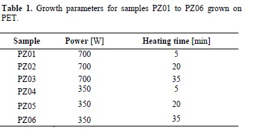
The ZnO nanowires obtained were characterized by three techniques: scanning electron microscopy, X-ray diffraction and optical transmission. SEM system was operated at 5 kV in order to obtain the ZnO nanowire images with a secondary electron detector in a Zeiss MOD Auriga 39-16 microscopy. The X-ray diffraction patterns were measured in Grazing-incidence small-angle X-ray-scattering (GISAXS) with Xpert PRO Diffractometer from panalytical using Cu radiation (Kα=1.54 Ǻ). Optical transmission measurements were obtained with a Spectrometer UV/VIS Lambda 35 PERKIN ELMER in the region of 300 nm to 1100 nm. Table 1 shows the growth parameters for the ZnO nanowires samples.
3. Results and Discussion
Figure 1 shows the X-ray diffraction patterns of the samples PZ01 to PZ06. In these, ZnO nanowires were grown on substrates of polyethylene terephthalate (PET) at different conditions of thermal treatment in a microwave furnace. Crystalline phases are identified as zinc oxide (ZnO) and PET. The thermal treatment was performed at 350 W and 700 W varying the time from 5 min to 35 min. When the furnace power was 350 W and the treatment time was 20 min and 35 min, the intensity of the reflections of ZnO in the address (100) has the highest intensity. For applying a heating time of 5 min, the intensity of the reflections of ZnO, in the addresses (100), (002) and (101), were the highest. When the furnace power was increased to 700 W and the heating time was 20 min, the highest intensity was obtained for the reflection (002). Furthermore, applying 35 min of heating time, leads to obtain the highest intensity in the reflection (100). On the other hand, the thickest film was obtained when the furnace power was 700 W and 20 min of heating time. The signal of the PET substrate can be observed even to high power and large heating time in the furnace. However, the thickness of the film is not thick enough to block the substrate signal. In the thermal treatment conditions studied, the growth of ZnO nanowires is performed preferentially in the directions (100) and (002).
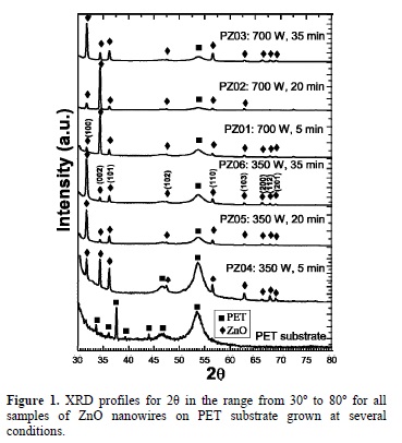
Figure 2 shows the SEM images of the ZnO nanowire arrays grown at 700 W for 5, 20 and 35 min on PET substrate with scale bar of 200 nm. The growth of the nanowires aligned vertically on the substrates is clearly observed, besides the hexagonal cross section of the wires. We observed similar results as in our previous work [12] on the influence of the heating time on the diameter size. Increasing heating time, ZnO nanowires grow with smaller diameter. The diameters vary approximately from 150, 100 and 50 nm for a heating time of 5, 20 and 35 min, respectively.
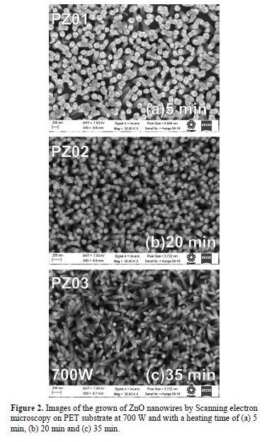
Figure 3 shows the SEM images of the ZnO nanowire arrays grown at 350 W for 5, 20 and 35 min on PET substrate with scale bar of 1 µm. Although we observed a vertically aligned growth of the nanowires for a heating time of 5 min, for a heating time of 20 min the nanowires grew parallel to the substrate. Besides, the growth at 20 min shows also ZnO structures like bars with diameters larger than the nanowires. For a heating time of 35 min (sample PZ06), the nanowires show an almost vertical alignment but with a decrease in their density.
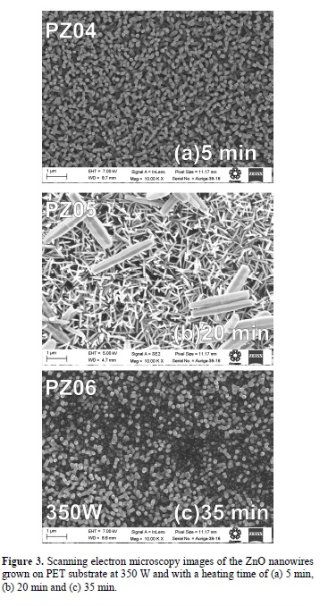
Figure 4 shows the optical transmission spectra in the range of 300 nm and 1100 nm for all samples at room temperature. Sample PZ04, which was the thinnest film according to X-ray diffraction patterns shows the highest transmission, contrary to sample PZ02 which was the thickest film showing the lower transmission.
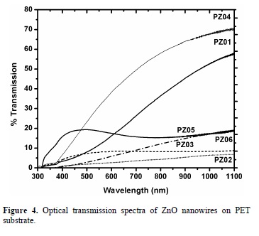
From the transmission spectra the energy gap was obtained from each sample. It was no possible to determine the bandgap energy of the sample PZ05 through this method. Table 2 shows these results.
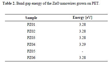
In general, it can be observed that there is not so much variation in the value of the bandgap energy, which remains constant independently of the conditions of the growth parameters. Sample PZ04 showed the best value of the bandgap energy which is the closest to bulk ZnO of 3.37 eV.
4. Conclusiones
ZnO nanowires are grown on PET substrate by the hydrothermal method, using a rapid process of heating by microwave. In high power (700W) and varying the heating time of 5 to 35 min the growth of ZnO nanowires on PET is favored. A correlation between the heating time and the diameter of nanowires was observed. For larger heating time, smaller diameter is obtained in the nanowires. The value of the bandgap energy remains almost constant independently of the growth parameters.
Acknowledgments
This work was financially supported by Instituto Politécnico Nacional, México under Project Nr. 20131553.
References
[1] Z. L. Wang, J. Phys: Condens. Matter 16, R829 (2004). [ Links ]
[2] K. Keis, L. Vayssieres, H. Rensmo, S. E. Linquist, A. Hagfeldt, J. Electrochem. Soc. 145, 2920 (1998). [ Links ]
[3] C. X. Wang, G. W. Yang, C. X. Gao, H. W. Liu, Y. H. Han, J. F. Luo, G. T. Zou, Carbon 42, 317 (2004). [ Links ]
[4] X. Y. Kong, Z. I. Wang, Nanolett. 3, 1625 (2003). [ Links ]
[5] C. Y. Lee, S. Li, P. Lin, T. Y. Tseng, IEEE Trans. Nanotechnol. 5, 216 (2006). [ Links ]
[6] Martins R., Fortunato E., Nunes P., Ferreira I., Marques A., Bender M., Katsarakis N., Cimalia V., Kiriakidis C., J. Appl. Phys. 96, 1398 (2004). [ Links ]
[7] W. I. Park, G. C. Yi, M. Y. Kim, S. J. Pennycook, Adv. Mater. 14, 1841 (2002). [ Links ]
[8] L. E. Greene, M. Law, J. Goldberger, F. Kim, J. C. Johnson, Y. Zhang, et al. Angwe. Chem. Int. Edn. 42, 3031 (2003). [ Links ]
[9] L. Vayssieres, Adv. Mater. 15, 404 (2003). [ Links ]
[10] M. Law, L. E. Greene,, J. C. Johnson, R. saykally, P. D. Yang, Nat. Mater. 4, 455 (2005). [ Links ]
[11] H. E. Unalan, P. Hiralal, N. Rupesinghe, S. Dalal, W. I. Milne, G. A. J. Amaratunga, Nanotechnology 19, 255608 (2008). [ Links ]
[12] Concepción Mejía-García, Elvia Diaz-Valdés, Gerardo Ortega-Cervantes, Esteban Basurto-Cazares, J. Chem. Chem. Eng 6, 61 (2012). [ Links ]

